UNIVERSITY
OF TRENTO
DEPARTMENT OF INFORMATION AND COMMUNICATION TECHNOLOGY
38050 Povo – Trento (Italy), Via Sommarive 14 http://www.dit.unitn.it
O
PTICALP
ACKETS
WITCHINGW
ITHP
HOTONICC
RYSTALS:
A
NO
VERVIEWCarlos Bilich
www.carlosbilich.com.ar
June 30
th, 2005
Abstract—All optical packet switching arises as the last
research frontier of optical networking. It is desirable because of several reasons being the most important the necessity to eliminate the bottleneck that constitutes electro-optical conversion. Having all optical packet switching networks without electro-optical conversion is the way to go to provide the astonishing amounts of bandwidth requirements needed for a future network that will link people, places and objects. So far, somehow “traditional techniques” based on per-packet wavelength routing, deflection routing, optical burst switching, etc., have been proposed without much commercial success. Aside for these approaches based on smart architectures, there are others based on novel devices like molecular electronics and photonic bandgap materials among others. Of particular interest among bandgap periodic structures, are photonic crystals. This article describes their properties and how they can be used to build a photonic packet switch.
Index Terms—all optical packet switching, photonic crystals,
photonic bandgap structures, optical routing, optical data processing.
I. INTRODUCTION
HE idea of an all optical packet switching (OPS) network, scalable and commercially viable, has been around among optical telecommunications researchers for a long time, so far without much success, at least from the commercial point of view. The backbone of today’s network architecture it is based on an electro-optical infrastructure where the transport is mainly optical and processing is electronic. This is a very flexible architecture which also has a benefit of performing signal regeneration, including reshaping, retiming and re-synchronization. However, the costly part of this type of approach is the Optical-Electrical-Optical (O-E-O) conversion both in terms of price and performance. O-E-O constitutes one
Manuscript received June 30, 2005. This work was done as paper project for the Ph. D. course on “Satisfying QoS Requirements over Single Packet
Switching Networks” held at the Department of Information and
Communication Technology of the University of Trento, between March 29-April 15, 2005, corresponding to the academic year 2004/2005. Taught by Prof. Yoram Ofek, Marie Curie Chair Professor at Department of Information and Communication Technology of University of Trento.
C. G. Bilich is with the Center of REsearch And Telecommunication Experimentations for NETworked communities (CREATE-NET) and a Ph. D. Student at the International Graduate School in Information and Communication Technologies, University of Trento, Trento, TN 38100 Italy (corresponding author phone: +39-0461-828584; fax: +39-0461-421157; e-mail: [email protected]).
of the main bottlenecks for tomorrow’s high capacity networks. Experts predict savings of up to 75 percent in network costs as a result of eliminating unnecessary O-E-O conversion elements [1]. Having an infrastructure composed of all optical elements will also eliminate costly upgrades by enabling continuing functionality with increasing line rates, new protocols, and new wavelengths.
Among a myriad of alternatives that have been proposed over the years two emerge as the most recently actively researched: optical packet switching [1]-[5], and optical burst switching [6]-[8]. Optical packet switching exploits single wavelength channels as shared resources, and thru the usage of statistical multiplexing of traffic flows, manages the great amount of bandwidth available in WDM systems. Two main solutions emerged as a result of this approach: broadcast-and-select and wavelength routing architectures. However, both of them use fiber delay lines (FDL) at some stage of the architecture. FDLs are strict FIFO queues with fixed delays, i.e., do not permit random access. Also, to be able to resolve contention effectively, a large number of FDLs are usually required and handling many fibers in a node can be a difficult task. Optical signals delayed in FDLs suffer from power loss and therefore there is a need for optical amplifiers. The problem of the accumulated noise due to the usage of cascaded amplifiers severely limits the network size at high bit rates.
A solution proposed to overcome some of these technological limitations is optical burst switching (OBS). In OBS the basic units of data transmitted are bursts, made up of multiple packets, which are sent after control packets. The job of the control packets is to reserve the necessary resources on the intermediate nodes of the transport network. This results in a lower average processing and synchronization overhead than OPS since packet-by-packet operation is not required. However this approach has a comparably low degree of statistical resource sharing which lead to a less efficient bandwidth utilization.
Aside from these architectural methods based on known and available technologies, there are other approaches based on breakthrough technologies that can lead to new devices. Examples are Micro-Electro-Mechanical Systems (MEMS), which are minuscule mechanisms sculpted from semiconductor materials with tiny tilting mirrors that can flap up and down in the optical equivalent of a cross-bar switch. Liquid Crystals, which are based on a technology similar to the one used in laptop screens in which the orientation of long molecules, and thus, the optical properties of the material can
Optical Packet Switching With Photonic
Crystals: An Overview
Carlos G. Bilich
switches, where heat is applied to one of the arms of a Y-splitter to change the refractive index, thus blocking the light traveling down that arm. Lithium niobate (LiNbO3) based switches in which a voltage controls the refractive index alterations that enable switching. But perhaps one the most promising direction is that of photonic bandgaps structures (PBG). These structures present a photonic energy bandgap similar to the electronic bandgap that made possible the construction of transistors. The idea of a photonic transistor using PBG materials is still in its infancy but even without it, primitive components based on PBG structures can be combined in a way that can be used to perform photonic switching. The aim of the article is to explore its potential utilization towards optical packet switching. The rest of the article is organized as follows: section II provides an overview of PBG structures which is especially focused on photonic crystals; section III describe a possible architecture and section IV concludes with some future trends.
II. PHOTONIC CRYSTALS
A. General idea
Photonic crystals are artificial structures that manipulate beams of light in the same way silicon and other semiconductors control electric currents, i.e. they present a so-called band gap. The electronic band gap is a forbidden zone, a narrow range of energies that electrons cannot occupy. When the electrons in the semiconductor fill all the states available to them below the band gap, electric current cannot flow, because each electron has nowhere to go; and boosting an electron above the gap takes a lot of energy. However, if there exist some excess electrons, they automatically must sit above the gap, where they can easily roam through the wide open spaces of empty states. The same happen when a deficit of electrons opens up some positively charged “holes” below the gap, again providing a way for current to flow readily. The switching and logic functions of semiconductors come from the possibility to control the availability of electrons and holes above and below the band gap. The existence and properties of an electronic band gap depend crucially on the type of atoms in the material and their crystal structure, i.e. the spacing and shape of the lattice that they form. In turn, its properties can be tailored by adding dopants that substitute various other atoms into the lattice or its interstices. Photonic bandgap materials involve similar structures but a larger scale, because while in Si and other semiconductors adjacent atoms are separated by about a quarter of a nanometer; in PBG the spacing is about three orders of magnitude bigger.
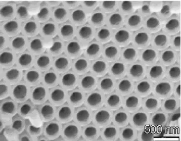
Fig. 1 shows a typical example of PBG structure represented by a block of special glass drilled through with a closely spaced array of cylindrical holes, each with a diameter between 400 and 500 nanometers. These openings are analogous to the atoms in a semiconductor. Light entering the holey material will refract through and partially reflect off the myriad internal interfaces between air and glass [9]. The
complex pattern of overlapping beams will reinforce or cancel one another out according to the light’s wavelength, its direction of travel through the crystal, the refractive index of the glass, and the size and arrangement of all the holes. Perfect cancellation in all directions for a narrow band of wavelengths would act similarly as the electronic band gap, i.e., that band of light cannot propagate through the crystal. On the other hand, modifying the band gap structure, (e.g. by filling some holes) is similar to what can be done by doping electronic semiconductors; and since often a photonic crystal is made of an electronic semiconductor material, the structure presents both an electronic and a photonic band gap.
B. Considerations and findings
It is worth to notice that although the term “photonic” makes reference to light, the band gap principle applies equally well to any form of electromagnetic radiation. In fact in electronic semiconductor crystals, the band gap arises because the electrons behave indeed partially like a wave, and these waves scatter off the layers or rows of the crystalline structure formed by the atoms. As a consequence, the electron’s wave is reflected back completely, like hitting a mirror. In order to have a full band gap, this perfect reflection must occur over a range of wavelengths and for waves heading in any direction through the crystal. In the case of light, the scattering is caused by changes in the refractive index in the interface of two materials, for example, air and glass. In this condition, an interaction similar to the one manifested by electrons would call for a material with an extraordinary high refractive index (RI) (e.g., higher than 4), something that is very difficult since few materials with such a high RI exist in nature [11]. Fortunately, formation of complete PBG is not only a question of large refractive index contrasts. The choice of an appropriate symmetry and topology plays a very important role as well, because the band gap depends on how the waves interact with many hundreds holes in a very complicated process [9], [11]. Schrödinger’s equations governs electrons while Maxwell’s equations
Fig. 1. Photonic crystals obtained by stibnite inverse opal method [10].
describe the behavior of light, therefore, in order to find the right arrangement of holes, previous theoretical methods developed for semiconductors where not useful. On the other hand, there is the effect of polarization which cannot be neglected in photonics the same way it is done in electronics. Finally, Ho et al. [12] published a work in which they demonstrated that a diamond structure (Fig. 2) should show the “missing” gap. A band gap occurs in the diamond
structure for a refractive index as small as 1.87 while many optical materials are available with refractive indices as high as 3.6. But perhaps the most important consequence of this discovery is that the diamond structure has a tetrahedral geometry, which is precisely that of Si, a material that is widely available and already easy to manipulate. Fig. 3 shows a comparison between the geometries of atoms in Si and dielectric spheres forming a diamond lattice with their associated bandgaps.
C. Defects
As it happens with semiconductors, the interest of photonic crystals with a complete PBG (cPBG) would be limited without the inclusion of controlled defects. A defect creates allowed states for particular photon frequencies in the band gap. For example, a line defect within a photonic crystal can guide photons through the system. If the frequency of light lies within the cPBG, it will have to be confined to the defect
line since propagation is forbidden through the rest of the photonic crystal. Such a property has been exploited to build commercial photonic crystal fibers [14]. The advantage of such a system over conventional optic fibers or waveguides is that in this case, light confinement does not rely on total internal reflection. Therefore sharp bends should not present any transmission losses.
Point defects are of paramount importance for spontaneous emission inhibition and light localization. A point defect consists of an imperfection created deep in the bulk of the crystal. It can be obtained by removing one of the building blocks, changing its refractive index or modifying its size. Fig. 4, taken from [15] shows an example of the effects on the band structure of a point defect in a square lattice of dielectric rods. In this case defects are created by varying the radius of the cylinders. When the defect involves the removal of dielectric it is called air defect and an allowed mode appears close to the bands below the cPBG (also called dielectric bands) and evolves towards bands above the cPBG (air bands). Conversely, defects involving dielectric addition are called dielectric defects and the cavity mode evolves from air to dielectric bands as dielectric is added. Point defects can be
regarded as cavities in which light can be trapped and their size and topology can be designed to tune the frequency of the resonance.
D. Applications
Among many of the application envisioned for this technology it was already mentioned the possibility to build optical fibers that can be sharp bent with no losses. Also the fact that these fibers have a hollow core reduces the absorption and nonlinearities, thus enabling transmission at higher power. Photonic crystals can also be used to build a perfect channel drop filter, where the rerouting of the desired channel into the drop waveguide is done with 100% transfer efficiency (i.e., no losses, reflection or crosstalk), while leaving all other channels in the bus waveguide unperturbed [13]. They can also be used to build splitter and waveguide intersections operating at 100% efficiency, and finally, as it will be discussed in the following section, they can be a key technology to enable all optical packet switching.
Fig. 2. The diamond lattice that was the first that presented a complete photonic band gap.
Fig. 3. Conceptual analogy between photonic crystals structures and semiconductor materials [13].
Fig. 4. Point defects in a square lattice made of dielectric rods (radius=0.2a). Depending on the radius (r) of the point defect, localized states are created within the cPBG [11], [15].
A. The Passive Optical Limiter
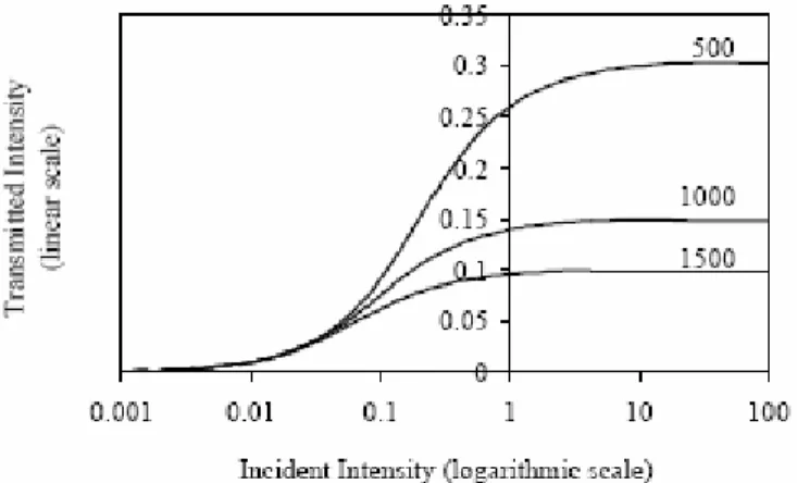
In electronics a limiter is a nonlinear electronic circuit whose output is limited in amplitude and it is generally used to limit the instantaneous amplitude of a waveform, i.e. to clip off the peaks of a waveform. Analogously, a passive optical limiter is a device that limits the intensity of a beam of light so that the power of the light exiting the side opposite the incident end, asymptotically approaches a limiting value as incident power is increased. Fig. 5 shows the
intensity-dependent optical response of a passive optical limiter. An optical limiter can be engineered so that it clamps the output level below a design-specific limiting intensity, in this way as the strength of the incident intensity is increased, the transmittance decreases and the width of the stopband gets larger.
One way to realize optical limiters is thru the utilization of nonlinear periodic structures, such as photonic crystals. As it was explained in previous sections, the spectral position, strength, and bandwidth of a photonic stopband depend on structural and material parameters such as refractive index contrast and lattice geometry. Incorporation of an optical nonlinearity causes the refractive indices, and therefore the response of a crystal, to vary with intensity [17]. A device whose behavior depends on the intensity of a control signal, or even the information signal itself, may potentially serve to process information in optical form, as it will be shown next.
B. Addition-based signal processing
Optical limiters provide a prospective basis for optical signal processing. They can be used to filter, shape, and multiplex optical pulses and to limit the optical power, as it was explained before. Devices based on optical limiting find application in ultrahigh-speed networks and in specialized high-speed processors such as data and signal regenerators and encryptors. Passive optical limiters are also commonly used as protective devices [18]. For the purpose of this article it is particularly interesting to describe how the passive optical
number of optical logic functions [16]. The derived optical logic functions make use of a ternary logic system, in which normalized power levels of 0, 1, and 2 are each discretely valued in the system and enable the implementation of a complete logic set. This unconventional logic functions are the result of photon-photon interactions occurring by nature through a material. In [19] it is shown that the basic set of
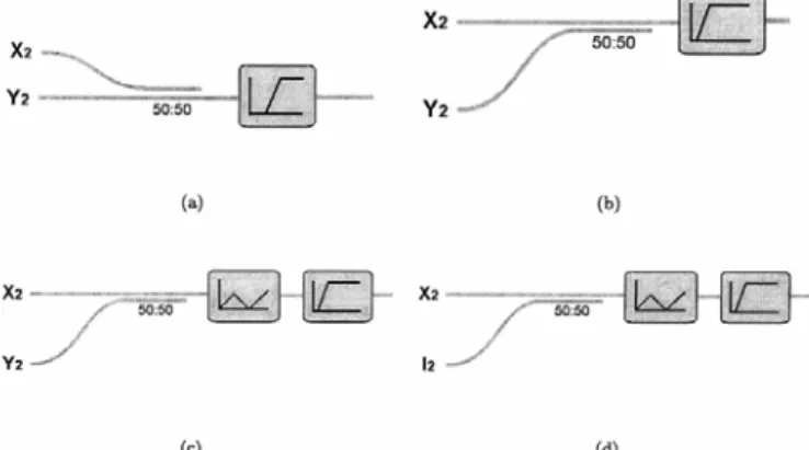
transfer functions showed in Fig. 6 can be closely obtained with optical limiters. The transfer functions shown in Fig. 6 allows signal interaction to occur through summation alone, and device output is determined by the input at a single port which is subjected to a limiting transfer function.
Fig. 7 illustrate how hard optical limiters with the transfer functions illustrated in Fig. 6 can be used for the construction of OR and AND gates. Using a 3dB coupler, inputs A and B are combined into a single beam. The transmitted intensity is defined as the O1 output and the reflected value as the O2. If one of the inputs is 0 and the other 1, the output at O1 is 1 and at O2 is 0. If both A and B inputs have the value of 1, a 1 is transmitted and 1 reflected. Thus, O1 yields the result of an
OR operation and O2 the result of a digital AND.
The interconnection of devices exhibiting this behavior alone can provide a complete logic set. Reference [19] shows this complete set which is in turn reproduced in Fig. 8. Therefore these functions provide the complete framework to design systems based on this signal addition-based signal processing scheme. As well as producing a complete combinational logic system, the previously-mentioned optical
Fig. 5. This plot illustrates the transition between low and high incident intensities as well as the saturation to a limiting value. All of the devices clamp the transmitted intensity to a limiting value [17].
Fig. 6. Basis set of transfer functions that can be obtained with optical hard limiters. IIN must be thought as the summation of I1 + I2. (a) AND (b) OR.
[16], [19].
Fig. 7. Logic OR and AND gates. For two input beams A and B, the transmitted intensity of the hard limiter implements the OR function while the reflected beam implements the AND operation. [17].
limiting devices provide two further all-optical logic functions: the optical sampler and the optical segregator. These new logic blocks allow the execution of
non-combinational logic and data separation based on intensity level.
C. Sampler and Packet Forwarder Design
In [19] Johnson et al., further explored noncoherent addition signal processing through the design and study of a sample-and-hold device and a packet forwarder, using only the basis set of transfer functions shown before. The design of the noncoherent addition-based sampler presented in [19] is based on its analogous electronic D-type flip-flop. Its layout is
shown in Fig. 9. The design behaves as follows: when the clock signal, CLK, is high, the output varies in proportion with the value presented at the input. When the CLK signal goes low, the feedback from the output is the selected output value. This value then persists at the output until the CLK signal is made high again. This provides an optical sampling function where the input value is sampled at the moment that the CLK signal falls. The key elements of the sampler are the inversion operation and the presence of a short delay in the feedback loop. The inversion operation produces a high signal at the input of one of the AND gates when the CLK signal is low. This selects the feedback signal and suppresses the input signal when the CLK is low. The feedback delay allows the output to be selected before the low CLK signal propagates through the system.
The other building block necessary to build the packet forwarder is an optical segregator. This device separates the
two non-zero intensity levels in the ternary logic system {1,2} into two intensity levels onto two separate lines. The block diagram representation of this device is shown in Fig. 10.
To exploit the functionality of these two devices, the packets are formed as in Fig 11. In this packet design, the frame bit is assigned a different intensity level, than the address and data bits. This enables the separation of the co-propagating frame bit using the segregator. The packet router uses the segregator to separate the packet from its framing bit. This will allow a very simple address recognition scheme and circumvents the need for synchronization.
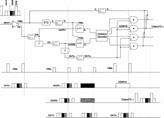
So far, all the elements required for a packet forwarder where described. These blocks are then combined to come up with an experimental design of a packet forwarder that can be used to perform the following operations in all optical domain:
• extraction of framing bit,
• extraction of addressing information, • address decoding,
• routing of packet onto decoded path, • reassembly of packet and framing signal.
A schematic of the whole system is depicted in Fig. 12. Briefly, it works as follows: Once the frame signal has been separated, the address information is extracted by temporally aligning parts of the signal with the framing bit by subjecting copies of the signal to preset time delays. The lengths of these time delays are determined by the data rate of the system. They are set so that the address bits are at the flip-flop inputs when the clocks go low. The stored address information is decoded according to the preset routing scheme which is implemented using the combinational optical logic described in the previous sections. The packet, without the framing bit, then propagates down the correct path as determined by the output address bit. The framing bit, with intensity level 2, then rejoins the packet. It is worth to notice that with the packet design shown in Fig. 11, the system is self clocking and needs no external synchronization. The framing bit gives the reference time against which the arrival times of the rest of the bits are measured. The relative positions of the synchronization, address, and data portions of the packet are
Fig. 8. Connection of devices to achieve (a) AND, (b) OR, (c) XOR, and (d) NOT layout. [19].
Fig. 9. Layout of logic gates to enable sampling operation using noncoherent addition of signals. This design relies most heavily on the availability of the inversion operation and the signal restoration module [19].
Fig. 10. Block diagram of an optical signal segregator [16].
Fig. 11. Composition of a packet to be routed all-optically. The separation of the data and address bits is enabled by the leading framing bit. [19].
completely arbitrary, and are only determined by the setup of the system. For more details on the performance of this system design, the interest reader can consult the work of Johnson et al., in reference [19].
IV. CONCLUSION
This overview showed how a breakthrough technology based on novel periodic structures called photonic crystals can be used to revolutionize optical packet switching. The article reviews the whole process, starting from an explanation of the device physics, its functional principles and how it works. Then it was showed how the necessary building blocks are made, and finally how all these components can be used to build a system architecture that could satisfactorily perform all optical packet switching. Due to the versatility of these new devices, it is almost sure that the future of all optical packet switching will take advantage of them in some way or another, and this is why this work seems pertinent at these early stages of the development.
ACKNOWLEDGMENT
The author would like to thank Prof. Edward (Ted) H. Sargent, MIT’s Visiting Professor - Nanotechnology and Photonics, for his guidance and for his valuable suggestions something without which, this work could not have been possible.
REFERENCES
[1] M. A. Bourouha, M. Bataineh, and M. Guizani, “Advances in optical switching and networking: past, present, and future,” in Proc. IEEE
SoutheastCon 2002, 2002, pp. 405–413.
[2] S. Yao, B. Mukherjee, and S. Dixit, “Advances in photonic packet switching: an overview,” IEEE Commun. Mag., vol. 38, no. 2, pp. 84– 94, Feb. 2000.
[3] D. K. Hunter and I. Andonovic, “Approaches to optical internet packet switching,” IEEE Commun.Mag., vol. 28, no. 9, pp. 116–122, Sep. 2000. [4] L. Xu, H. G. Perros, and G. Rouskas, “Techniques for optical packet switching and optical burst switching,” IEEE Commun. Mag., vol. 39, no. 1, pp. 136–142, Jan. 2001.
[5] M. J. O’Mahony, D. Simeonidou, D. K. Hunter, and A. Tzanakaki, “The application of optical packet switching in future communication network,” IEEE Commun. Mag., vol. 39, no. 3, pp. 128–135, Mar. 2001. [6] C. Qiao and M.Yoo, “Optical burst switching OBS—a new paradigm for
an optical internet,” J. High Speed Networks, vol. 8, pp. 69–84, 1999. [7] C. Qiao, “Labeled optical burst switching for IP-over-WDM
integration,” IEE Commun. Mag., pp. 104–114, Sep. 2000.
[8] M. Yoo and C. Qiao, “Optical burst switching for service differentiation in the next generation optical internet,” IEEE Commun. Mag., vol. 32, no. 2, pp. 98–104, Feb. 2001.
[9] E. Yablonovitch; “Photonic Crystals: Semiconductors of Light”;
Scientific American (International Edition), vol. 285, no. 6, pp. 47-55,
December 2001.
[10] Juarez, B. H., Ibisate, M., Palacios, J. M. & Lopez, C.; “High-energy photonic bandgap in Sb2S3 inverse opals by sulfidation processing.”;
Adv. Mater. 15, 319, 2003.
[11] García Santamaría, F.; “Photonic crystals based on silica microspheres”; Ph. D. Thesis, Instituto de Ciencia de Materiales de Madrid; 2003. Available: http://users.mrl.uiuc.edu/floren/Thesis/Chapter_1.pdf [12] Ho, K. M., Chan, C. T. & Soukoulis, C. M.; “Existence of a Photonic
Gap in Periodic Dielectric Structures.”; Phys. Rev. Lett. 65, 3152; 1990. [13] Johnson, S. G., “Photonic Crystals: Principles, Techniques, and
Applications”; MIT Applied Mathematics, [online]. Available: http://ab-initio.mit.edu/photons/tutorial/
Fig. 12. Schematic of a packet forwarder based on noncoherent signal-addition logic. The packet forwarder separates the framing bit from the packet and uses this signal to trigger the flip-flops, recording the value of the header bits. These bits are decoded to select the correct output port and the packet is forwarded. [19].
[14] Soljacic, M.; “Omni-Guide Photonic Crystal Fiber: From Theory to Production.”, MIT Physics Dept. & Omni-Guide Communications Inc.; Photonic Crystal Workshop; April 18- April 22, 2005.
[15] Joannopoulos, J. D., Villeneuve, P. R. & Fan, S. H.; “Photonic crystals: Putting a new twist on light.”; Nature 386, 143, 1997.
[16] Johnson, E.; Brzozowski, L.; Sargent, E.H.; “All-optical time-domain IP router using optical limiters”; Lasers and Electro-Optics Society 2000
Annual Meeting. LEOS 2000. 13th Annual Meeting. IEEE; vol. 1, pp. 33
– 34, 2000.
[17] L. Brzozowski and E. H. Sargent; “Photonic Crystals for Integrated Optical Computing,” Optical Society of America - Optics in Computing,
Quebec, QC, pp. 786-796, 2000.
[18] L. Brzozowski and E. H. Sargent; “Optical Signal Processing Using Nonlinear Distributed Feedback Structures,” IEEE Journal of Quantum
Electronics, vol. 36, no. 5, pp. 550-555, 2000.
[19] E. Johnson, E. H. Sargent, "Function and sensitivity of signal processing systems based on addition followed by limiting," Journal of Lightwave
Technology, vol. 20, no. 8, pp. 1388-1396, 2002.
Carlos G. Bilich was born in Santa Fe, Argentina in 1971. He
graduated as Electro-Mechanical technician from the Superior Industrial School in 1990. Then he moved to Rosario to study Electronic Engineer at the National University of Rosario, and graduated in 1997. He was working in industry even before graduation as a network system engineer at Carrefour S.A. Soon after his graduation he was appointed as an automation engineer at Techint Corporation for his flat steel division in Argentina, named SIDERAR, where Mr. Bilich implemented several control models for the electric furnaces and water cooling lines of the hot steel rolling mill. In 1999 he was recipient of a Fulbright scholarship award to do his master degree in Telecommunications at the University of Pittsburgh. In 2001 he was at SIDERAR but as a semi-senior network engineer of the systems department. He was involved in performance measuring and tuning of the company intranet as well as working closely with software developers to aid in the design of distributed application that can meet the stringent performance standards of the company. By that time he was also chief architect of the automatic measuring system that was developed to monitor the performance of the J2EE and Microsoft distributed applications developed in SIDERAR. Recently, in 2004 he won a scholarship to pursue a Ph. D. in computer networks and mobility from the University of Trento, Italy. While doing his Ph. D. Mr. Bilich also works as a junior scientist at the Center for REsearch And Telecommunication Experimentation for NETworked communities, CREATE-NET; an International Research Center founded by a group of leading Universities and Research Centers of Europe and America, leading by the renowned Professor Dr. Imrich Chlamtac. Mr. Bilich primary research interests include: Pervasive computing technologies for healthcare, wireless networks, distributed applications and breakthrough technologies for all packet switching photonic networks.
![Fig. 4. Point defects in a square lattice made of dielectric rods (radius=0.2a). Depending on the radius (r) of the point defect, localized states are created within the cPBG [11], [15]](https://thumb-eu.123doks.com/thumbv2/123dokorg/2948693.23308/4.918.74.446.770.1034/defects-square-lattice-dielectric-radius-depending-localized-created.webp)