ROBERTO PAGANO
OPERATIVE PARAMETERS
OF Si PHOTOMULTIPLIERS
Coordinatore: Prof. G. Giaquinta
Tutor: Prof. G. Falci
Supervisori: Dott. S. Lombardo
Dott.ssa S. Libertino
Tesi per il conseguimento del titolo di dottorato
XXII-Ciclo
Chapter 1
Silicon Photomultipliers: principles and features
………... 8§ 1.1 Introduction to photodetectors………...9
— 1.1.1 Vaccum photodetectors………..10
— 1.1.2 Semiconductor photodetectors………...12
§ 1.2 SiPM History………...………..19
§ 1.3 Description and principle of operation………...………...24
§ 1.4 SiPM Properties……….………....32
— 1.4.1 Photon Detection Efficiency (PDE)………...32
1.4.1.1 Quantum Efficiency (QE)………...………33
1.4.1.2 Triggering Probability (Pt)………36
1.4.1.3 Fill Factor ( εgeo)………..………..38
— 1.4.2 Gain………40
— 1.4.4.Noise………...42
1.4.4.1 Primary Dark Counts………..43
1.4.4.2 Afterpulsing……….……….44
1.4.4.3 Crosstalk………..46
— 1.4.5 Timing……….49
— 1.4.6 Dynamic Range………...49
— 2.2.1 Forward Current………..63
— 2.2.2.Reverse Current………...68
§ 2.3 Gain……….76
— 2.3.1 Transient Current Measurement Mode………...76
— 2.3.2 Photocurrent Measurement Mode………...84
§ 2.4 Dark currents………...90
§ 2.5 Conclusions………...95
Chapter 3
SiPM Characterization
………96§ 3.1 Fabrication detail………..………..97
§ 3.2 Small SiPM array electrical characterization...…………..………...100
—3.2.1 Forward current…...…….………..100
—3.2.1 Reverse current………….………..104
§ 3.3 Dark current model: from single pixel to SiPM……….……..…110
§ 3.4 Technological issue………..113
§ 3.5 Other devices: the Hamamatsu MPPC……….……..121
§ 4.2 X-rays irradiations………...………..………...134
— 4.2.1 Electrical characterization...………..134
— 4.2.1 Optical characterization……….…………..………..136
§ 4.3 Ion implantation………..……….……….138
§ 4.4 Heavy ion irradiation………...……….…141
— 4.4.1 Br irradiations……...………141
— 4.4.3 Au irradiations……...………146
§ 4.5 Conclusions………...………...……….…152
APPENDIX
………155A Light Absorption in semiconductors………...…155
B Current in a p-n junction……….160
C Thesis results ……….163
Silicon Photomultipliers (SiPMs) are a very promising alternative to conventional photomultipliers (PM) thanks to some interesting characteristics: they are insensitive to magnetic fields, hence can be used in environments with high fields; their operation voltage is far lower, and they ensure better robustness and reliability than PM; they are much cheaper than their traditional counterpart.
SiPM structure consists in a parallel array of equal single pixels, each one made of a silicon p-n junction avalanche photodetector with an integrated resistor. The SiPM is biased above the breakdown voltage, that is, each pixel is operated in Geiger mode, above the breakdown voltage (BV) of the p-n junction. The junction is carefully doped in order to have breakdown only in the central active area of the pixel, used for the photon detection, and by the avalanche mechanism (not by Zener). To understand the photon detection concept, let us assume to bias such junction above breakdown with a fast voltage step. In this condition, if no carrier is present in the depletion region the junction is highly sensitive to the detection of single photons. In fact, if the photon is absorbed by creating an electron-hole pair, both carriers will start to drift in the high field region of the depletion layer and, being the voltage above breakdown, this drift will result with a 100% probability in the impact generation of a second e-h pair, and so on, up to the build-up of the junction avalanche. The avalanche is limited by the buildup of a limiting space charge in the depletion layer which decreases the field Moreover, since the photodetector has a resistor in series, when the avalanche current flows through the resistor, the voltage applied to the junction drops below BV. It quenches the avalanche, the current decreases to zero, and the voltage across the p-n junction increases again above BV. The pixel is ready again to detect the arrival of a new photon. Clearly, all the
transients recorded are the result of both capacitive effects and (generally faster) avalanche build-up characteristic times.
Such ideal picture is strongly modified by the occurrence of phenomena leading to dark current, generally attributed to generation effects from Shockley-Read-Hall (SRH) defects in the depletion layer, afterpulsing effects, and diffusion of carriers from the quasi-neutral boundaries of the p-n junction .
The purpose of this work was to understand the behavior of dark current in single pixels of SiPMs. Chapter 1 introduces the field of research. It reports the most important characteristics that photomultipliers must have and a brief comparison between traditional photomultipliers and SiPM. A brief history of SiPM invention and devolution is also discussed.
Chapter 2 reports a detailed experimental characterization of single pixels. In particular, current voltage (I-V) characteristics in both forward and reverse biases were collected. The careful analysis of the data allowed us to obtain information on the junction quality (ideality factor) and on the behavior in the operation range. Moreover, by taking into account the contribution given by the avalanche build-up and quenching and the effect of generation / diffusion of carriers in the depletion layer, we provided a detailed understanding of the I-V curves. We also proposed a physical model of the I-V above breakdown voltage able to reproduce the voltage and temperature dependence of the current for the studied devices, still in Chapter 2.
The current-voltage characteristics of matrixes from 5×5 pixels up to 64×64 pixels (pre-commercial devices) are reported in Chapter 3. In this chapter some fabrication issues are also shown: the uniformity problem, the effect of the presence of optical trenches (introduced to improve the structure performances) and the importance of the substrate dopant.
Finally, Chapter 4 reports some preliminary results on the effect of irradiation on the devices. In particular, measurements were performed after irradiating the devices with different species: X-rays, light ions (Boron) and heavy ions (Brome and Gold)
SiPM: principles and features
The ability to detect single photons represents the ultimate goal in optical detection. To achieve such sensitivity a number of technologies have been developed and refined to suit particular applications. These include: Photomultiplier Tubes (PMTs), Microchannel Pate Photomultiplier Tubes (MCPMT), Hybrid Photon Detector (HPD), p-i-n photodiodes, linear and Geiger mode Avalanche Photo Diodes (APDs) and much more. The need for ever more sensitive, compact, rugged and inexpensive optical sensors in the visible region of the spectrum continues today, and is particularly acute in the fields of the biological sciences, medicine, astronomy and high energy physics. Applications such as fluorescence and luminescence photometry, absorption spectroscopy, scintillation readout, light detection and ranging and quantum cryptography require extremely sensitive optical sensors often in adverse environments, such as high magnetic fields, and where space is limited.
In many of these applications the PMT has become the detector of choice. However, since its inception in the 1980's, the so-called silicon photomultiplier (SiPM) has begun to rival the PMT in many of its parameters such as gain, photon detection efficiency and timing. In addition, the SiPM has all the additional benefits of silicon technology such as compactness, high volume, low cost production.
In the next sections we will briefly introduce the photodetectors characteristics, we will then discuss the history of SiPM birth, its operation principle and properties and, finally, we will get a look on some application fields.
§ 1.1 Introduction to Photodetectors
Photodetectors are electronic devices that give an electrical output signal in response to a light input signal. They are essential elements in any optoelectronics system and their importance is comparable to the light source.
The genesis of photodetectors can be ascribed to the discovery of the photoconductivity (1873 by W. Smith) [1]. Great breakthroughs occurred with the discovery of the photoelectric effect by Millikan and its interpretation by Einstein in 1905 [2] and with the introduction of the quanta hypothesis to solve the blackbody emission [3-4] by Planck. Since then, different and equally important devices were invented. The most popular are the photoelectric vacuum-tubes, including the photomultiplier tube (PMT), and the semiconductor photodetectors.
A photodetector is generally characterized by different properties, which are normally the average value of a statistical distribution [5]. Since all of them will be widely discussed in the following sections of this chapter, here they will be only listed, and they are:
• Quantum efficiency (QE or εQ): it is the probability that a photon incident on the
active surface of the detector generates a photoelectron. (0<εQ<1).
• Collection efficiency (CE or εC): it is the probability that a generated photoelectron
start the electron amplification mechanism (0<εC<1)1.
• Gain (G): it is the mean value of the charge produced by the internal electron amplification mechanism per photoelectron generated.
• Dark Current or Dark Noise: it is the electrical current produced by the internal noise mechanisms of the photodetector in dark condition (i.e. when no photons strike the sensitive area of the detector).
1 The term photon detection efficiency (PDE) is often used for the combined probability to produce a photoelectron and to detect it (PDE=εC⋅εG).
• Dynamic range and Linearity: it is the maximum signal produced by the detector without a significant distortion with respect to the input signal.
• Response time: this includes the transit time, that is the time elapsed between the photon arrival time and the electrical output response of the detector, and the transit time spread, which contributes to the pulse rise time and the duration.
• Single photon detection capability: it is important when measuring very low photon flux.
• Rate Capability: it is the maximum rate for photon detection and it is inversely proportional to the time needed, after the arrival of a photon, to get ready to detect the next.
• Stability: essential for long term operation at elevated counting rate.
Before starting the description of Silicon photomultipliers, the object of this thesis, it is fundamental to briefly review the most diffused photodetector used in ultra-weak photon detection.
1.1.1 Vacuum photodetector
In a vacuum photodetector the photocathode and the electron multiplication stage are enclosed in a vessel made of glass or ceramics. Vacuum photodetector are of three types: photomultiplier tube (PMT), microchannel plate photomultiplier tube (MCP) and hybrid photodetector (HPD).
The PMT was proposed almost 100 years ago, in 1919, by J. Slepian [6] and the first real device was demonstrated by Iams and Salzberg in 1935 [7] and by Zworikyn in 1936 [8]. PMT has been unrivaled by semiconductor photodetectors in the single photons detection field for long time, thanks to its good response speed and its very low excess noise. Up to now, PMTs are widely used in many applications where a low photon flux must be detected.
Figure 1.1: (a) PMT’s typical format [9]; (b) Basic structure of a PMT.
They are fabricated in different formats (some examples are shown in Figure 1.1 (a) and very large sensitive area up to 50×50 cm2 can be realized.
The basic structure of a photomultiplier tube, shown in Figure 1.1 (b), is composed of a photocathode (mostly in transmission, sometimes in reflections2), an electron optics (missing in slow units and in compact devices), a dynode chain that yields a high internal gain of charge multiplication, an anode (output electrode) to collect the amplified charge. A bias voltage of hundred Volts is applied between the photocathode and the first dynode, as well as between the successive dynodes. Such high voltage is needed to ensure that the photo-emitted electrons will hit the next electrode with adequate energy for the multiplication (~100 eV), and that the collection efficiency will be close to the unity.
The photocathode is a thin semiconductor film, with a suitably low work function. When a photon impinges on the photocathode sensitive surface an electron is generated by photoelectric effect. This photoelectron is then accelerated by the high electric field and guided (focused) by the electron optics to hit the first dynode. At the first dynode, the primary photoelectron produces the emission of g electrons from the dynode, by a phenomenon know as secondary emission. Secondary electrons leaving the first dynode are accelerated to the second dynode, where they produce g2 electrons, and so on up to the last dynode. For n dynodes, at the anode we will find gn electrons. The gain (G) is gn, is very high even for a
2 In a reflection photocathode the electrons are emitted from the same side surface on which photons impinge, in a transmission photocathode the electrons are emitted from the opposite side surface.
moderate g: for example, for g=4, with n=8...14, we get G=6·104…2·107, respectively. The current collected at the anode is in the order of few mA even for a single photon detected and can be directly processed with standard electronic instrumentations. The total gain depends on the applied voltage U as G=AUkn, where k ∼ 0.7 ⎯0.8 (depending on the dynode material), n is the number of dynodes and A is a constant (which also depend on n).
The sensitive wavelength range covered by a PMT depends on the photocathode material (long wavelength cut-off) and on the light enter window material (short wavelength cut-off).
Despite of the complex amplification process, the response to the light impulse is relatively fast, few nanosecond duration. The critical drawback of PMTs is their sensitivity to external magnetic field (sometimes even to the geomagnetic one). It deflects electron in flight from their standard trajectory causing a loss in the efficiency and in the gain and an increase in the time spread Δτd. A high-permeability metal shield is often necessary to allow operation in
moderate fields, up to ∼ 0.1T. Moreover, since the electrode structure is not so rugged, photomultipliers are not immune to vibrations, that could induce the modulation of the gain during normal operation. Finally, the high bias voltage required (1000 ⎯ 2000V) between the anode and the cathode induces a high power consumption.
In a MCP the discrete dynode chain is replaced by continuous multiplication in 6-20 μm diameter cylindrical holes, or channel (Figure 1.2 (a) and (b)). These channels are densely
Figure 1.2: (a) Microchannel plate photomultiplier tube, (b) electron multiplication in a
packed in few mm thick glass plate. The inner channel walls are processed to have proper electric resistance and secondary emission properties. The multiplication gain depends exponentially on the ratio of the channel length to its diameter. A typical value of this ratio is 40, and a typical gain of a single microchannel plate is ∼ 104. For higher gain to or more channel plates are used in series. MCP offer good spatial resolution, excellent time resolution (∼20ps) and can tolerate axial magnetic fields exciding 2T. However, they suffer of a relative long recovery time and a short lifetime.
HPD combine the sensitivity of a vacuum PMT with the excellent spatial resolution of a
Si detector [11]. The
photoelectron is accelerated trough a potential difference of ∼ 10÷20 kV before hits the silicon sensor as shown in Figure 1.3. The electric field is usually shaped in such away that the entry light is de-magnified onto the silicon sensor that can be smaller than the window. The gain is smaller than in typical PMT and a low-noise amplifier must be used to read out when low photon flux must be detected. HPD also requires high bias voltage and it can’t work in magnetic field.
Figure 1.3: Hyprid photon detetctor. The larger
photocathode surface isimaged onto a much smaller Si sensor by a suitable shaped electric field [12].
1.1.2 Semiconductor Photodetectors
Semiconductor photodetectors were developed after the Second World War thanks to the progresses obtained in the comprehension of their physics and to the improvement in the control of their technology. Semiconductor detectors are solid-state devices exploiting the internal photoelectric effect, as opposed to photoemission effect of vacuum photodetectors. In them, the charge-carries pairs generated by photon absorption contribute to electrical conduction internal to the device, and to a corresponding current at the contacts of external circuit. Thus, in a semiconductor photodetector, detection and production of photoelectrons take place in the same thin material.
Absorption of photons will depend on the semiconductor characteristics (for a detailed discussion on photon absorption in semiconductors see APPENDIX A). In order to generate a charge carrier pair in the semiconductor material, photons need to have sufficient energy hν>E, where E is the energy that must by supplied at the expense of the photon energy hν. This condition leads to a long wavelength cutoff λc=hc/E for the absorbed photon wavelength. Concerning the energy E suitable for photon absorption, in intrinsic semiconductor, where the photon absorption produces a transition of an electron from the valence band into the conduction band, E is equal to EG, the energy gap of the semiconductor. In extrinsic
semiconductor energy levels in the forbidden-gap are involved in the carrier generation. The long-wavelength cutoff then will depend on the energy level position in the bandgap. In silicon, that is an intrinsic semiconductor, photon with wavelength shorter than about 1050 nm (i.e with energy exceeding the silicon bandgap Eg=1.12 eV) can create electron-hole pairs
by the photoelectric effect.
A silicon photodiode, in its simplest form, is a reverse-biased p-n junction (as shown in
Figure 1.4: Representation of a p-n
junction photodiode, the photo-generated charge transport mechanism and the optical transmitted power.
Radiation is incident on the p-type region which carrier the ohmic anode contact, a metallization shaped as a ring around the access window to avoid optical obstruction. The p region is made relatively thin, by doping it more heavily than the n region, so that photons have a good chance to cross it and be absorbed in the depleted region of the junction.
The charge carriers (electron and hole) generated by absorption of photons with energy hν≥EG, decrease exponentially with depth z like the optical power (see Figure 1.4). The main contribution to photogenerated current comes from the pairs generated in the depleted layer. Here, electrons and holes are separated by the electric field and by drift they reach the neutral-charge regions where they are collected by the electrodes.
The PIN photodiode is the most common type of photodiodes used in low light detection. It is an intrinsic piece semiconductor sandwiched between two heavily doped n+ and p+ regions (Figure 1.5). The reverse bias increases the thickness of the depleted region. This has two benefits with respect to other devices: the decrease of electronics noise due to a lower capacitance and an improved sensitivity at higher wavelengths because the absorption length (Figure 1.6) is comparable to the thickness of the sensitive region (typical 100μm). The
Figure 1.5 Structure of a p-i-n avalanche photodiode and its
electrical field for a reverse polarization.
quantum efficiency can exceed 90%, but decreases towards longer wavelengths because of the increasing absorption length of light in silicon.
Figure 1.6 Absorption coefficient α and
absorption length 1/α in silicon
semiconductors.
Since there is no electron multiplication (G=1), amplification of the signal is needed. Low light level signal detection is
limited to a few hundred photons even if an amplifier is used.
Avalanche photodiode (APD’s) have similar structure of regular photodiodes, but they are operated at a much higher reverse bias. This allows each photo-generated carrier to get multiplied in an avalanche, resulting in an internal gain (typical G=10÷200) within the photodiode [13]. As a result, a detectable electrical response can be obtained from low intensity optical signals, as low as 10÷20 photons. Well designed APDS have achieved photon detection efficiency of ∼70% with sub-ns response time [14].
The sensitive wavelength window and the gain depend on the semiconductor used. Stability and monitoring of the operating temperature are important for the linear-mode operation and cooling is often necessary.
The APD can also be biased at voltage larger than the breakdown voltage resulting in a infinity gain operation. An external load of high value limit the maximum current to a safe mode. This working regime is called Geiger Mode, since the APD is more akin to a Geiger-Muller counter. With an APD working in GM mode, we can get an output pulse for each detected photon. It has to be noted that in GM-APD, also called, SPAD (Single Photon Avalanche Detector) one ore more photons produce the same output pulse.
Since the devices discussed in the rest of this work are particularly designed APDs working in GM, most of the photodiode characteristics, such as the multiplication gain M, the quantum efficiency, noise, will be better discussed in the following sections, referring to those devices.
Compared to traditional vacuum-based detector, semiconductor detectors have several advantages. They are compact and robust, do not require high voltages, and are insensitive to magnetic fields. An other advantage is the low cost due to the relative inexpensive production method.
In Table 1.1 are compared the most relevant characteristics of the vacuum and semiconductor photodetectors discussed and those of a Silicon Photomultiplier, the argument of this thesis.
§ 1.2 SiPM History
The Silicon Photomultiplier (SiPM) is the last born in the family of solid state photodetectors and the research and development to reach better performances is ongoing.
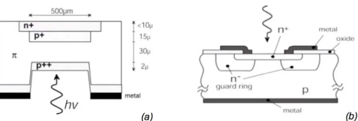
The first pioneers in the development of a solid state detector working in the so called Geiger mode, that is, biased over the breakdown voltage, were R. J. McIntyre and is coworkers at the RCA company and R. H. Haitz and his colleagues in the Shockley research laboratory, during studies on the physics of avalanche multiplication with high electric field intensity in semiconductor devices [15-16]. This was at the beginning of the sixties of the last century. The work of McIntyre and Haitz led to a basic insight in the phenomenon of avalanche breakdown, the physical phenomena involved in the avalanche buildup after the arrival of a photon, and in dark-current pulses. They provided important insight for the modeling of the behavior of the device operating in Geiger mode [17-18]. The two test structures fabricated and described by the two groups are shown in Figure 1.7. These structures were not conceived as photodetectors, and their performances were indeed severely limited by the technology available at that time for silicon devices. The main problems derived from the instability of the breakdown over the whole sensitive area of the detector. In fact, only a small volume of silicon could be depleted for the long time needed to detect photons due to the presence of many defects created during the fabrication process.
Only with the improvement of the fabrication technology, it was possible to fabricate the first planar Single Photon Avalanche Diode (SPAD) and the Super-low k APD structure (SLIKTM,used nowadays in the Single Photon Counting Modules SPCM produced by Perkin Elmer Optoelectronics [19]). The quenching of the breakdown voltage was obtained using a large external resistance, like in the Geiger counter, that reduces the voltage applied to the junction below the breakdown value so that it quenches the spread of the avalanche current. In this way the recovery time, i.e. the time needed to quench the avalanche and restore the
Figure 1.7: The first two prototypes of silicon single photon detector. (a) The reach-trough
structure realized at the RCA company by McIntyre group. (b) The planar n+p junction operating in Geiger mode developed at the Shockley laboratory by Haitz.
voltage over the breakdown value, was slow. The maximum counting rate that could be achieved was smaller than 100 kHz. The development of active quenching circuits, started in the eighties, allowed to improve the SPAD counting rate to more than 1 MHz, thus reducing the recovery and dead time [20-21].
The next logical step was to try to fabricate many individual single photon avalanche diodes quenched either in passive mode (i.e. with an external resistor) or in active mode (i.e. using an integrated quenching circuit) in a single silicon wafer. At the end of the nineties, the RMD company (Radiation Monitor Devices Inc.) developed an array of 6×14 avalanche photon diodes operating in Geiger mode with single photon avalanche capability. It was used for the detection of internally reflected Cherenkov light. Each APD was quenched using an active quenching circuit [22].
At the same time, in Russia was invented the MRS APD (Metal Resistor Semiconductor Avalanche Photodiode). It consists of a p+n or an n+p junction designed to work over the breakdown voltage with a thin metal layer on the top of the structure (Ti~0.01 µm) covering a resistive layer made with SiC or SiXOY (30-80 MΩ cm). The resistive layer on the top of the junction realized the negative feedback in the local area of the multiplication process to switch off the avalanche: the avalanche process increases the current through the resistive layer at the silicon interface redistributing the potential in the structure. This causes a
Figure 1.8: Scheme of different Metal Resistor Semiconductor (MRS) structures with single
photon detection capability in the light and near UV wavelenght: (a) MRS structure with SiXOY resitor layer from [23], MRS structure with SiC resistive layer from [24].
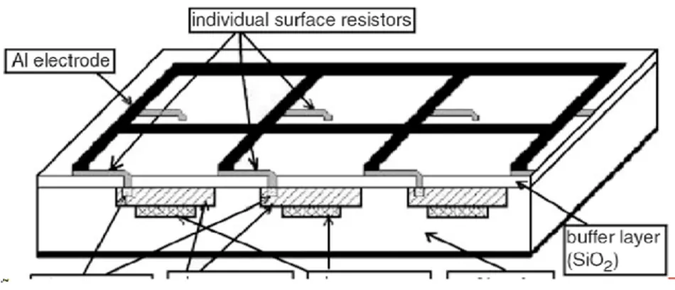
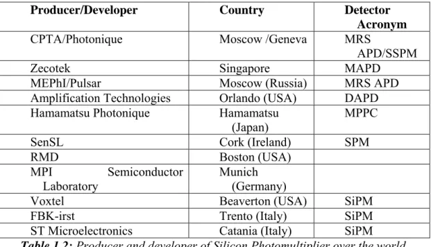
deceleration of the avalanche process itself and finally its termination. It is to be noted that the resistive layer negative feedback has a local nature due to a very low tangential conductivity of the resistive layer. In Figure 1.8 are shown two examples of different MRS structures; the first has an SiXOY resistive layer consisting essentially of SiO2 interspersed with amorphous silicon (Figure 2a), and the second with a SiC resistive layer, (Figure 2b). The resistive layer on the top of the Silicon surface is an important feature of the structure. As already said, it performs the quench of the avalanche process by a local negative feedback, thus stabilizing the avalanche process itself. At the same time it realizes an electrical decoupling agent between adjacent identical structures. This allows the production of a large numbers of microcells in a very fine structure on a common substrate with common electrodes, as shown in Figure 1.9. This structure represents therefore the birth of the silicon photon multiplier. Key personalities in this development were V. Golovin [25] and Z. Sadygov [26]. The technology for producing the SiPM is compatible with the standard Metal Oxide Silicon (MOS) process and promises the realization of sensors with a great area and a large number of micro cells at low cost of fabrication. From this initial seed, many different configuration and structures have been proposed and numerous new developments are ongoing. Nowadays, a few first generation devices are commercially available, but the level of maturity of the conventional PMT has still not been reached. In Table 1.2 are listed all the producers that are
involved, till today, in the fabrication and development of this sensor. Every producer uses its own name for this type of device (for a complete list of the names used see Table 1.3) but the basic structure of all the commercially available sensor is the same and it is reproduced in
Figure 1.10. Devices with up to 40.000 cell/mm2 are nowadays available.
Figure 1.9: Basic structure of Silicon Photomultiplier (SiPM) taken from [26].
Figure 1.10: Schematic cross section of a SiPM. Each pixel has an individual surface
Producer/Developer Country Detector Acronym
CPTA/Photonique Moscow /Geneva MRS
APD/SSPM
Zecotek Singapore MAPD
MEPhI/Pulsar Moscow (Russia) MRS APD
Amplification Technologies Orlando (USA) DAPD
Hamamatsu Photonique Hamamatsu
(Japan) MPPC
SenSL Cork (Ireland) SPM
RMD Boston (USA)
MPI Semiconductor
Laboratory Munich (Germany)
Voxtel Beaverton (USA) SiPM
FBK-irst Trento (Italy) SiPM
ST Microelectronics Catania (Italy) SiPM
Table 1.2: Producer and developer of Silicon Photomultiplier over the world.
Acronym Extended Name
SiPM Silicon Photomultiplier
MRS
APD Metal Resistor Semiconductor Avalanche Photodiode
MAPD Micro-pixel Avalanche Photodiode
MPPC Multi-Pixel Photon Counter
SPM Silicon Photomultiplier
SSPM Solid State Photomultiplier
PPD Pixelated Photon Detector
DAPD Discrete Amplification Photon Detector
AMPD Avalanche Microchannel Photodiode
GM-APD Geiger Mode Avalanche Photodiode
§ 1.3 Description and principle of operation
The Silicon Photomultiplier, as already said, is a pixilated photon detector, formed by a matrix of independent cells. Each cell (or pixel) is connected to the others by metal grids so to
have common contacts. In Figure 1.11(a) a photograph of a real commercial silicon
photomultiplier produced by Hamamatsu Photonique with an area of 3×3 mm2 is shown. The schematic structure of the SiPM is proposed in Figure 1.11(b): a matrix of N×N cell is fabricated on a common substrate (the yellow layer). The active volume of the device, where photons are mainly absorbed and the carrier pairs produced are multiplied by the intrinsic mechanism of amplification of the device, is confined in a few microns under the top surface (white layer). Finally a metallization grid is fabricated on the top of the structure in order to connect all the N×N pixels each to the others. The single cell (a schematic cross section is shown in Figure 1.11(c) is essentially an APD operating in the Geiger mode (GM-APD) with an integrated resistor in series whose goal is double: the quenching of the avalanche breakdown when the cell is fired by an incoming photon and the isolation between adjacent cells. To better understand the working principle of the whole detector it is helpful to briefly discuss the physics involved in the amplification of photons in an APD and the operation in Geiger Mode.
Figure 1.11 (a) Photography of a SiPM produced by Hamamatsu Photonic (MPPC
S10931-050P) with 3×3 mm2 area. (b) Schematic view of a SiPM structure. (c) Cross section of a single cell.
In an APD the weak light detected is internally amplified The avalanche multiplication by impact ionization is the mechanism that allows the photogenerated carriers amplification. The avalanche is obtained by applying a high reverse bias voltage to the photodiode, so as to bring it into the breakdown region usually avoided in normal operation.
The structure we will use to describe the multiplication process is, for simplicity, a p-i-n avalanche photodiode, schematically shown in Figure 1.5. In a p-i-n avalanche photodiode, as previously discussed, an intrinsic region i, is fabricated between the p+ and the n+ regions. The electric field (E) in the intrinsic region i, when the diode is reverse polarized, is constant and equal to the maximum Emax. When a photon impinging on the open window of the device is
absorbed, it creates an electron-hole pair. The high electric field accelerates the photo-generated carriers, raising them to a kinetic energy large enough to ionize the crystal lattice with the subsequent production of electron-hole pairs. The new pairs are accelerated and multiplied as well, originating a process named avalanche multiplication. If M is the total number of pairs produced by an initial photoelectron, the output current (I) is I = MIph, where
Iph is the total photocurrent produced by the absorption of an incident radiant power P.
In silicon, the charge carriers multiplication process is described by the ionization coefficient α and β of electrons and holes, defined as the number of new pairs generated for unit length by the carrier at a given electric field E.
Figure 1.12 shows the curves of α and β as a function of the electric field in silicon. As it is evident, starting from 105 V/cm, the ionization coefficient increases dramatically even for a small increment of the electric field, while for E < 105 V/cm ionization is negligible. It has also to be
Figure 1.12 Ionization coefficient of
electron α and hole β as a function of the electric field for silicon.
noted that in silicon the ionization of electrons is more efficient than for holes [28].
To evaluate the low frequency avalanche gain, M, of the avalanche photodiode, we assume a multiplication structure of length W, with a uniform field, as it is shown in Figure 1.13, so that α and
β are constant. Let’s assume that a primary electron is photogenerated at x=0 and that the amplified current is collected at x=L.
Figure 1.13 Avalanche multiplication in a
uniform electric field starting from a primary electron injected at x=0. If ie and ip are the electron and hole current at x, their increment along an elemental path dx
is proportional to α and β and to the current itself:
die
dx =α⋅ ie+β⋅ ih ,
dih
dx = −
(
α⋅ ie+β⋅ ih)
(1.3.1)Solving Equations 1.3.1 with the boundary condition ie(0)=Iph, ie(L) = I = MIph and
ih(L)=0, we obtain the avalanche multiplication gain of the APD (M), as follow:
M=(α−β)exp
[
(
α−β)
W]
α−βexp
[
(
α−β)
W]
(1.3.2)The gain M depends on the applied reverse voltage through the field dependence of the ionization coefficient α and β (see Figure 1.12). In silicon, as already discussed, the coefficient α>>β, thus leading to a simplified expression of Equation 1.3.2. In general, for α≠β, the gain always become infinite when exp(α-β)W=α/β. This condition can be obtained by incrementing the bias voltage over the breakdown voltage, VBD, of the APD. An APD in
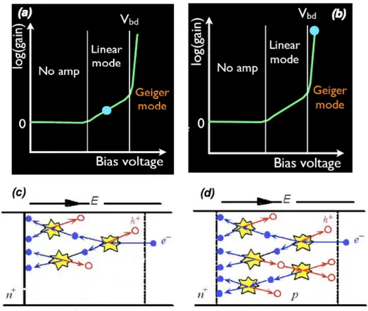
fact can be operated in two different modes: in linear mode and in Geiger mode. Common APDs are fabricated to work in linear mode. The multiplication gain, in this condition, is finite and can be tuned by varying the applied voltage. The mean number of multiplied carriers per photogenerated electron is constant and depends on the bias voltage. This mode of operation, illustrated in Figure 1.14 (a) and (c), is named linear since the number of collected carriers is proportional (by a factor M) to the number of absorbed photons.
When the applied bias voltage exceeds the breakdown voltage VBD, the APD would enter
into the Geiger mode operation. In this condition, the electric field across the junction is so high that the multiplication mechanism brutally increases and tends to infinite. Electrons and holes have enough energy to allow multiple ionizations in the crystals lattice. This
Figure 1.14. Gain as function of the bias voltage for an APD working in linear mode (a) or in
Geiger mode (b). The number of multiplied carriers by impact ionization when polarized above the VBD is finite (c) while tends to infinite when polarized over the VBD (d).
process is self sustaining and the output current is in the order of the milli-Amperes [29]. The Geiger mode of operation is shown in Figure 1.14 (b) and (c).
If an APD operated in Geiger mode is connected to the bias voltage through a large resistance, RQ, as illustrated in Figure 1.15 (a), the Geiger discharge would be quenched
because the effective bias voltage at the APD terminals drops below VBD. This is the basic
structure of the single pixel of the Silicon Photomultiplier. In Figure 1.15 (b) it is shown its electrical scheme.
A circuit model, which emulates the evolution of the signal of a GM-APD in series with a quenching resistance, was developed in the1960s to describe the behavior of micro-plasma instabilities in silicon [16]. According to this model, the pre-breakdown state can be represented as a capacitance (the junction capacitance, CD) in series with the quenching
resistor. Referring to Figure 1.15 (b) this state corresponds to the switch in the OFF condition. In steady state, the capacitance is charged at VBIAS>VBD. When a carrier crosses the high-field
region, there is a certain probability, known as turn-on probability, to trigger an avalanche circuit a voltage source VBD with a series resistor RS in parallel to the diode capacitance
Figure 1.15. (a) Schematic representation of the single pixel of the SiPM. (b) Equivalent
discharge. If this happens, the new state of the system can be represented by adding to the (switch closed in Figure 1.15 (b)). RS includes both the resistance of the neutral regions inside
the silicon as well as the space charge resistance. CD, originally charged at VBIAS>VBD,
discharges through the series resistance down to the breakdown voltage with a time constant
τD given by the product RSCD. RS is estimated to be much smaller than RQ. It should be noted
that the discharge current is initially limited by the build up of the avalanche process which can take some hundreds of ps. Since RS ranges from 100Ω to few kΩ, this time can be similar
to τD for small diodes. As the voltage on CD decreases, the current flowing through the
quenching resistance, and as a consequence through the diode, tends to the asymptotic value of (VBIAS-VBD)/(RQ+RS). In this final phase, if RQ is high enough, the diode current is so low
that a statistical fluctuation brings the instantaneous number of carriers flowing through the high-field region to zero, thus quenching the avalanche. The capacitance charged at VBD, starts
recharging again to the bias voltage with a time constant CDRQ, and the device becomes ready
to detect the arrival of a new photon. The typical output pulse, observed at RQ, is
schematically shown in Figure 1.16. The single pixel of the SiPM works exactly as a SPAD with an external quenching resistor in series. The main limitation of a SPAD is that the output signal is the same regardless of the number of incoming photons, i.e. it works as a binary device. In order to overcome this limitation, multiple pixels can be connected in parallel to a single output. The structure so obtained is properly the Silicon Photomultiplier. A schematic circuit representation of a SiPM is shown in Figure 1.17.
Figure 1.16. Output pulse shape at the
Figure 1.17. Schematic circuit representation of a SiPM with n cells.
Each pixel of a SiPM, when fired by a photon, works independently, producing the same output current pulse. When multiple photons hit the SiPM active area, the output signal is then the sum of each individual signal produced by the single pixels and, therefore, proportional to the number of cells hit by a photon. In this way the binary single device has been used to fabricate an analog device able to quantify the number of photons from a low intensity light source.
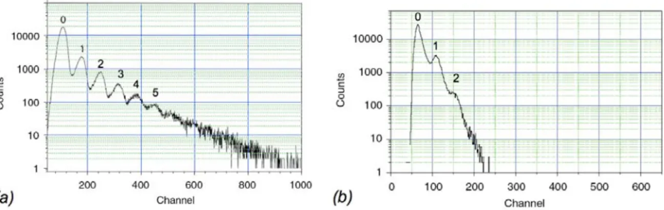
Using a simple linear amplifier, the output pulses of a SiPM can be observed on an oscilloscope or recorded with an Analogue to Digital Converter (ADC) with a fixed gate. In
Figure 1.18 (a) a typical oscilloscope screenshot of the output pulse of a 100 pixel SiPM produced by Hamamatsu is shown; Figure 1.18 (b) shows the histogram, the photoelectron spectrum, of the ADC output in response to repeated fast pulses of a weak light incident on the SiPM sensitive area. The first peak in the spectrum, the pedestal, is a measure of the noise in the system (detector+electronics) and corresponds to the moments in which no pulses were recorded during the gate time. The second peak of the spectrum or the first photoelectron (1 p.e) corresponds to a single pixel fired, the third peak to two simultaneous
Figure 1.18. (a) Oscilloscope screenshot of the signal produced by a SiPM with 100 pixels
when illuminated by a low-photon flux. (b) Photoelectron spectrum of SiPM recorded with ADC readout as a response of a low-photon flux reprinted from [30].
pixels fired (2 p.e) and so on. The straight separation between peaks and the good uniformity of the single peak demonstrates the good performance of the SiPM to detect a low photon flux.
§ 1.4 SiPM Properties
§ 1.4.1 Photon Detection Efficiency (PDE)
The Photon Detection Efficiency (PDE) of a SiPM is the statistical probability that an incident photon produces a Geiger pulse from one of the SiPM pixel i.e. the probability that a photon impinging on the sensor surface is detected. It is a function of the wavelength and of the bias voltage and it is defined as the product of three components:
PDE
( )
λ,V = QE(λ)⋅ Pt(V )⋅εGEO (1.4.1)where QE is the quantum efficiency of the photosensitive area (see next section); Pt isthe
triggering probability i.e. the probability that a photo-generated carrier has to trigger an avalanche breakdown; εGEO is the geometric fill factor of the device i.e. the ratio of the
photo-sensitive area to the total area of the sensor. Like other silicon-based
photodetectors, the silicon photomultiplier has a high quantum efficiency (QE), close to 100%, in the visible range. However, the overall photon detection efficiency for present state of the art SiPM is lower, due to other additional contribution apart from QE. All these factors have a relevant impact on the overall efficiency and must be
Figure 1.19. (a) Comparison of PDE for SiPM, APD
carefully optimized to maximize the overall PDE. Figure 1.19 shows the PDE for present state of the art SiPMs in comparison with the typical QE of PMTs and APDs. The SiPM PDE is at the level of the PMT QE for blue light and larger in the yellow-red region.
§ 1.4.1.1 Quantum Efficiency (QE)
The quantum efficiency of the photosensitive area represents the probability for a photon, impinging on the active surface of the detector, to generate an electron-hole pair in the active thickness of the device that could be trigger an avalanche breakdown. Not all the incident photons produce an e-h pair since not all the incident photons are absorbed. Some of them simply fail to be absorbed because of the probabilistic nature of the absorption process. Others may be reflected at the surface of the detector, thus further reducing the quantum efficiency. Furthermore, some electron-hole pairs produced near the surface of the detector could quickly recombine due to the abundance of recombination centers close by and are therefore unable to trigger a breakdown.
The quantum efficiency, can therefore be expressed as:
QE= (1− R)e−αw(1− e−αW) (1.4.2)
where R is the optical power reflectance at the surface, α is the silicon absorption coefficient (cm-1), w is the depth from the Si/SiO2 interface of the depleted region (cm) and W is the width of the depleted region (cm). The quantum efficiency is therefore an adimensional number (0<η<1) sometime expressed in percent.
The first term of Equation 1.4.2, (1-R), represents the effect of the reflection at the device surface. When light from a low refractive index medium, such as light in air (refraction index n0=1), impinges on the surface of a medium having a high refractive index, like silicon (nSi∼
3.5), a large portion of photons is reflected: 30% or more of the incident light is reflected causing a severe decrease of the detector QE. However, an anti-reflection coating on the
access window surface can appreciably reduce the reflection loss. This is obtained either with a single layer having a refraction index intermediate between n0 and nSi, or with a multiple
layer of materials, as in the standard anti-reflection coating (ARC) treatment of optical surfaces. Usually, a silicon detector is covered with a thin silicon dioxide layer (SiO2) having
a refraction index nSiO2∼1.4, which has a considerable influence on the reflection of photons at
the surface. Depending on the wavelength of photons, the reflected photons percentage can be reduced below 30%. Other materials, like Si3N4 (nSi3N4∼2), can improve the transmission of
light at the interface. A single layer on the surface can greatly reduce the reflection loss, but a significantly improvement on the light transmission at the interface can be obtained with a suitable coating made of several thin layers having different refraction index (ARC), as it is in commercially available devices. The reflection loss can be decreased down to values below 10% over the entire visible spectrum [32].
The second term in Equation 1.4.2, e-αw(1-e-αW), represents the fraction of the photon absorbed in the depleted region of the device. The photon flux absorbed in the silicon bulk at a depth z from the surface decreases exponentially with the following relation:
I(x)= I0exp(−αz) (1.4.3)
where I0 is the incident flux entering the silicon that has passed the passivation top layer, α is
the absorption coefficient of Si and z the depth from the Si interface. The carriers (electrons and holes) generated by the absorption of photons having enough energy (hν>Eg) decrease
exponentially with the depth z, like the photons flux. The main contribution to the Geiger count of photons comes from the pairs generated in the depleted region of the device. Electrons and holes, created there, are accelerated by the high electrical field and can trigger, by impact ionization, the breakdown. Conversely, electrons and holes created by photon absorption at depths between the Si/SiO2 interface and the boundary of the depleted region have a very short life time. In fact, usually the top layer of the photodiode is heavily doped, to reduce the series resistance and to ensure the electric field uniformity. This layer cannot be
depleted. Electrons and holes generated in that layer by photons absorption either recombine promptly or have to move by diffusion and can recombine with the abundant interface states.
Figure 1.20: Schematic structure of n on p
SiPM with the electric field and the transmitted photon flux as a fuction of the depht from the Si/SiO2 surface.
The carrier pairs generated in the quasi-neutral region beneath the depleted region are not as useful as those created in the depleted region. A minority carrier, as for example an electron in a p region, has, in fact, a high probability to recombine with a majority carrier, a hole in a p region, thus erasing the photon detection event. Only the pairs created close to depleted region within a minority diffusion length, Ln, can
move by diffusion to the high field region and then trigger an avalanche. This contribution is useful but much slower than that of carrier pairs generated into the depleted region since it entails the diffusion time constant of minority carriers τDn=Ln2/Dn with a characteristic time in the range of microseconds. At the time scale of the nanosecond, as in typical applications, shorter than that of diffusion motion, this contribution could be neglected. Therefore the fraction of charge pairs created to the absorbed photons and useful to trigger an avalanche is given by the fraction of photons dissipated in the range w - w+W, or:
αe−αzd w
w+W
∫
z= e−αw− e−α(w+W )= e−αw(
1− e−αW)
(1.4.4)In Figure 1.20 this situation is graphically represented.
The quantum efficiency of the active area can range from 80% to 90% depending on the wavelength but its maximum peak is relatively narrow with respect to the QE distribution of a PiN diode (see Figure 1.21) because the sensitive layer of silicon, i.e. the depleted region, is
Figure 1.21: Quantum efficiency of the active area as a function of the
wavelength for Hamamatsu 0-50-2 with 400 cells [33].
very thin (few micrometer). In the case show in Figure 1.21 the SiPM structure is a p-silicon on a n-substrate. The p layer is 0.5 μm on a 4 μm epitaxial layer [33].
§ 1.4.1.2 Triggering Probability (P
t)
A carrier that is moving trought a high-field region has a finite probability to trigger an avalanche breakdown. In the case of a photo-generation event, two carriers are created, an electron and a hole. In a high-field region the two carriers travel in the opposite direction and contribute together to the overall triggering probability that can be calculated from the following relation [34]:
Pt = Pe+ Ph − Pe⋅ Ph (1.4.4)
where Pe and Ph are the electron and hole initiation probability, respectively. These terms can
be calculated as a function of the generation position by solving two differential equations involving the carrier ionization rate, as follow:
dPe
dx = 1− P
(
e)
⋅αe⋅ P(
e+ Ph − PePh)
dPhdx = − 1− P
(
h)
⋅αh⋅ P(
e+ Ph − PePh)
(1.4.5) .
Pe(x) and Ph(x) are the probability that an electron or a hole generated within the depleted
volume of a pn junction, at the position x, triggers an avalanche breakdown, respectively. αe
and αh are the ionization coefficients for electrons and holes, respectively.
The total triggering probability Pt
can be calculated by integrating these equations with the boundary condition, in the case of a n+p junction, that Pe(0)=0 and Ph(W)=0,
where W is the width of the depletion region, that means that the probability to trigger an avalanche for a carrier coming from the high field region is zero. This calculation was performed by W. G. Oldaham [34] and the results for a n+p junction are shown in Figure 1.22.
The overall probability is then a function of the position where the pair is generated (voltage above breakdown) applied to the junction. As a thumb rule, to maximize the triggering probability and
Figure 1.22: Triggering probability for electron
and hole, Pe and Ph respectively for a n+p diode
operating ∆V above breakdown as a function of starting position x [34].
the PDE, the photogeneration should happen in the p side of the junction in order for the electron to pass the whole high field region and the bias voltage should be as high as possible. It has to be noted that the triggering probability Pt depends on the shape of the electric
field and, hence, on the doping profile. Special structures have been designed in order to maximize the triggering probability in such region were the creation of e-h pair is most probable (see for example [35]).
§ 1.4.1.3 Fill factor (ε
GEO)
Since the silicon photomultiplier is a pixilated sensor, some room between the cells is required for the separation, for the individual quenching resistor, for metallization (it connects all the pixels to the same electrode) and, sometimes, to fabricate the optical trenches that provide the optical isolation between the cells to prevent crosstalk phenomena (discussed in the following paragraph). The total area of the detector is, then, different to the sensitive area.
The geometrical fill factor, εGEO, of a silicon photomultiplier is defined as the ratio of the
photo-sensitive area (AS) to the total area (ATOT) of the device:
εGEO = AS
ATOT . (1.4.6)
Since the PDE of a SiPM has a strong dependence on the geometrical fill factor, it needs to be accurately optimized and, as we will discuss, the optimization depends on the application. In Figure 1.23 are shown some layouts of the single pixel of a SiPM produced by different developers. The total area occupied by a single cell is delimited with a white line while the sensitive area with a blue line. The currently achieved geometric fill factor in suitable models is in the range from 30% to 60%. As a rule, a SiPM with smaller pixel area has a smaller fill factor, therefore the best filling (and obviously the best PDE) can be obtained with a small number of large cells. Unfortunately, a SiPM with few large cells has a reduced linear
dynamic compared to a SiPM with the same total area but with a larger number of small cells. Also a big cell has a greater dark noise than a smaller one, since the dark noise is proportional to the depleted volume of the cell. The increase in area of the cell is limited by the maximum noise allowed in the particular application for which the SiPM is developed. Moreover, a large cell has a longer recovery time, since the time needed to restore the charge accumulated in a pixel is ∼ 4CDRQ,where CD is the capacitance of the cell and RQ is the quenching
resistance. The optimization of the fill factor, εGEO, of a SiPM is, therefore, a compromise
between the maximization of the PDE and the other performances required for the specific application. In those applications where a small number of photons must be detected, as for example in High Energy Physics (HEP) or in Astrophysics experiments, a high PDE is required, hence the best choice is to use a SiPM with few large cells i.e. with the greatest fill factor.
Figure 1.23: Fill factor for different structure: (a) Hamamatsu 25um cell size.
(b) SenSL 30um pixel. (c) FBK-Irst 40um cell sixe. (d) Hamamatsu 50 um cell sixe. (e) CPTA/Forimtek 50 um cell size. (f) ST Microelectronics 40 um cell size. The white line delimits the total area of the cell, the blue line the sensible area of the pixel.
On the contrary, in those applications where a large number of photons must be detected and the linear dynamic response of the SiPM is therefore much important, a SiPM with a lower PDE but with a large number of small pixels, i.e. with a worse fill factor but a better speed, is preferred. An example of the last application is the Positron Emission Tomography (PET). In PET the SiPM is coupled with a Lutetium Oxyorthosilicate (LSO) crystal that convert the 511 keV γ-ray emitted by the electron-positron annihilation into ∼15000 photons in the blue spectra. At the end face of the crystal, where the SiPM is mounted, thousands of photons must be collected. In order to avoid a saturation effect and to improve device speed, the number of cells into the SiPM needs to be large and, in turn, the cells must be small.
§ 1.4.2 Gain
One of the most important features of the SiPM is its intrinsic and stable high gain. The gain instability, observed in normal APDs, is due to the intrinsic statistical fluctuation of the avalanche multiplication process itself. On the contrary the SiPM, being operated in Geiger Mode, i.e. with M theoretically infinite, has a very stable gain. The stability of the gain is obtained thanks to the quenching mechanism provided by the series resistance. The suppression of the avalanche current by the negative feedback on the electric field trough the diode junction stabilizes the oscillation of the gain.
The gain of the SiPM is defined as the ratio of the output charge Qtot produced by nph
detected photons to the charge of an electron q:
G= QTOT
nph⋅ q (1.4.7)
Assuming that on average one photon produce the avalanche of one pixel, the gain is then given, referring to Figure 1.16, by:
G=Qpix q = IL q dt ≈
∫
CD(VBIAS−VBD) q (1.4.8)where CD is the diode capacitance and VBIAS-VBD is the applied overvoltage. Measuring the
charge delivered by one pixel is then possible to measure the gain of the SiPM. Since CD is
typically in the range of 10÷100 fF and VBIAS-VBD is in the range of a few volts, a high gain,
typically in the range of 105÷107, is obtained. The charge delivered by one pixel is commonly measured from the separation of peaks in the single photoelectron spectrum (Figure 1.18 (b)) providing the correct ADC channel to charge conversion.
Equation (1.4.8) provides a linear dependence of the gain versus the applied voltage and is the most common definition of the gain [30,31,33,35]. However, it was found that light emitted during the pixel breakdown penetrated adjacent pixels due to optical cross-talk (as discussed in the following paragraph 1.4.3.3) and fired these pixels. Thus the average number of pixels fired by a primary photoelectron is typically more than one. Then the real SiPM gain is equal to the charge QPIX multiplied by the average number of fired pixels to the
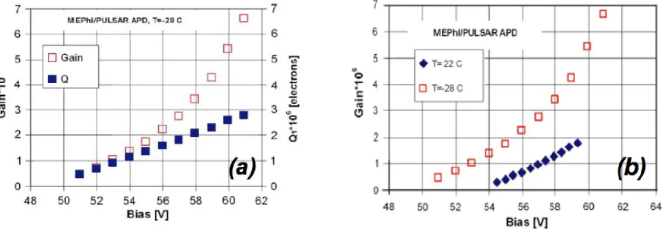
Figure 1.24: (a) Gain of a Mephi/Pulsar SiPM as a function of the bias voltage measured
from the charge delivered by one pixel, denoted as Q, and as the total charge, including the cross-talk effect, denoted as G. (b) Gain G as a function voltage at different temperature reprinted from [36].
electron charge. In Figure 1.24 (a) are compared the gain obtained measuring the charge delivered by one pixel (blue squares) and the real Gain (red squares) produced by a detected photons as described in [36].
The SiPM gain is also temperature dependent. As the temperature rise, the lattice vibrations in the crystal become stronger. This increases the probability that carriers may strike the crystal before the accelerated carrier energy has become large enough, and make it difficult for ionization to occur. Then, as the temperature rises, is required more energy from the electric field, i.e. a greater VBIAS, to produces an avalanche discharge as shown in Figure 1.24 (b).
§ 1.4.3 Noise
An avalanche breakdown in a SiPM can be triggered by a photo-generated carrier, when photons strike the detector, or by any free carrier generated inside, or near, the depleted region, even in dark condition. The pulses generated by these two processes are indistinguishable each other. The last one represents the intrinsic noise of the silicon photomultiplier and the frequency of such noise can be determined by counting the pulses occurring per second when the SiPM is in dark condition. The frequency of the noise is commonly named Dark Counts of the SiPM. The Dark Counts of a SiPM are due to the contribution of three components: the primary dark counts, the after pulsing and the cross talk.
A typical Dark Counts rate as a function of the threshold level of the readout electronics, normalized to the equivalent number of photo-electrons (p.e.), is shown in Figure 1.25 for a SiPM produced by Hamamatsu [37]. The rate of the dark pulses counted with a certain threshold corresponds to the number of pulses per second that have an amplitude larger than the threshold itself. The typical dark counts at room temperature (25°C) measured at a threshold of 0.5 p.e. range between 100 kHz to several Mhz per mm2. The count rate
Figure 1.25: Dark count rate as a function of the threshold level of the read out electronics,
normalized to the equivalent number of the photo-electrons, of a MPPC S10362-11-050C produced by Hamamatsu (1mm2 area) operated at a gain of 7.5·105 [37].
decreases considerably increasing the threshold of the readout electronics. Each increase of the threshold by the equivalent of 1 p.e. typically reduces the noise rate by almost one order of magnitude (Figure 1.25). Dark events with amplitude larger than 1 p.e are mainly due to the crosstalk phenomenon as discussed later.
§ 1.4.3.1 Primary dark count
The primary dark count is mainly due to thermally generated e-h pairs. It is the same phenomenon that causes the reverse current in ordinary p–n junction diodes, well interpreted by the Shockley–Read–Hall (SRH) theory [38-39]. In particular, it is well known that in silicon p–n junctions the reverse current is dominated by the generation in the depletion layer, whereas the contribution due the diffusion of minority carriers from the neutral regions to the junction is much lower (see Appendix B). According to the SRH theory, electron–hole pairs are generated in sequence through generation–recombination (G–R) centers, that are local levels at about mid-gap (Figure 1.26 (a)). Depending on the electric field profile of the device, it would be necessary to include the contributions due to the Poole–Frenkel effect and to trap-
Figure 1.26: (a) Thermally SHR generation of electron-hole pairs. (b) Field assisted
generation: (1) TAT and (2) SHR generation with Poole-Frenkel effect.
assisted tunneling (TAT) (Figure 1.26 (b)) [40]. The effect of TAT is to increase the emission rate of a G–R center. Similar considerations can be made for the Poole–Frenkel effect. In SiPM devices where the maximum electric field E is well below a critical value, these effects are estimated to be negligible.
The primary dark counts can be influenced by the SiPM production process aiming to minimize the number of generation-recombination centers (GR center), the impurity and crystal defects, wich give rise to the Shackley-Read-Hall effects.
§ 1.4.3.2. Afterpulsing
The afterpulsing is a detrimental component of the noise in a SiPM. In the silicon volume where the breakdown avalanche takes place, a high temperature (∼1000 °C) plasma is created. The generated free carriers can be trapped by deep level impurity states present in the depleted volume of the junction [41]. These trapped carriers may be released after a certain time Δt, as illustrated in Figure 1.27 (a), causing a delayed avalanche in the same pixel where breakdown occurred, i.e. an afterpulse (Figure 1.27 (b)).
Figure 1.27: (a) Trapping and delayed releasing of a free carrier produced during an
avalanche breakdown by a deep level impurity in the depleted volume of the junction. (b) Primary pulse and afterpulses reprinted from [42]
The typical timescale at room temperature is in a time ranging from 10 to 100 ns depending on the energy level of the impurity.
The afterpulsing probability Pap depends on both the voltage and the temperature. An
increment of the bias voltage produces an increase in the Pap since the gain enhancement
produces more electrons per avalanche, the triggering probability Pt increases and since the
emissivity increases due to the Poole-Frenkel effect. Operations at low temperature elongate the delayed release reducing the afterpulsing probability.
Afterpulses can strongly enhance the total dark count rate of a SiPM. Moreover, since they are related to the primary avalanche, which previously filled the traps, they are not randomly distributed, as a white noise, but are correlated. Its effect is then troublesome in any photon correlation experiment.
A simple strategy to reduce the afterpulsing contribution is to increase the recovery time of the pixels with a larger quenching resistance, in order to have enough time to depopulate the filled traps. Afterpulses occurring during the recovery time have amplitudes lower then 1
p.e (see Figure 1.27 (b)). If the threshold level of the readout electronic is opportunely chosen the extra counts due to afterpulses can be drastically reduced.
§ 1.4.3.3. Cross-talk
The cross-talk is a noise contribution common in all pixelated devices. A pulse current produced by a pixel, due to a photon detection event or to a primary dark noise event, can induce one or more adjacent pixels to experience the avalanche breakdown. The corresponding output pulse current of the SiPM has then an amplitude peak proportional to the number of involved pixels in the single photo-detection and in the correlated cross-talk phenomena. This noise contribution is detrimental in all the applications where the single photon resolution is required.
The cross-talk noise has two different physical origins: optical and electrical.
The optical cross-talk is due to the photons generation by radiative emission from the hot carriers produced during an avalanche discharge. In an avalanche multiplication process, on average 3 photons, with energy higher than the silicon band gap (1.14eV), are emitted every 105 carriers [43]. These emitted photons can travel to a neighboring pixel and trigger a
Figure 1.28: Optical crosstalk between neighboring pixels. Secondary photons emitted
during an avalanche discharge can reach adjacent pixels and trigger there an avalanche breakdown.
breakdown there, as illustrated in Figure 1.28, as any external photon. Several models were suggested in the past to explain the light emission as, for example, the breemsstralhung and a multi-mechanism scenario, including indirect and direct inter-band and intra-band transitions [43-47]. Particularly critical are the emitted photons in the spectral range between 850 nm and 1100 nm, because the photons with higher energy i.e. lower wavelength are all absorbed within the same cell and the infrared photons with wavelength larger than 1100 nm travel over long distances without being absorbed [48].
The electrical cross-talk can occur when carriers, generated during the avalanche breakdown in a cell, can cross the junction reaching a close pixel. Traveling along the epitaxial layer, common to all pixels, these carriers can reach the neighboring pixels and triggering there a new avalanche breakdown [49-50].
Some strategies have been studied to reduce the cross-talk between neighboring pixels. The first is to increment the distance between adjacent cells. This approach has a detrimental effect on the geometrical fill factor of the SiPM and a consequent reduction in the PDE is. The second strategy consists in fabricating grooves, filled with optical absorbing material, all around each cell. These grooves, commonly named trenches, prevent from optical and electrical coupling between cells. The reduction of the geometrical fill factor with
Figure 1.29: Crosstalk for 1.1 mm2 SiPM produced by MEPHI/Pulsar, measured as the pulse
such design is mild while the effect on the cross-talk noise is considerable, as shown in Figure 1.29 (a). Data of Figure 1.29 (b) evidence how the pulse height distribution is modified by the trenche presence: events with amplitude larger than the single pixel pulse amplitude are significantly attenuated.
The crosstalk noise has a strong dependence on the over-voltage and consequently on the gain, but it does not strongly depend on
temperature. The increase of the bias voltage above the breakdown value is reflected in an increase of the cross-talk probability. A typical of the SiPM at 1.5 p.e. over the dark count at 0.5 p.e., for different temperatures is shown in Figure 1.30, for an SiPM produced by Hamamatsu with 1 mm2 of sensible area.
over-voltage dependence of the cross-talk probability, measured as the ratio of the dark counts
A reduction of the crosstalk noise for the same cell area and fill factor can only be achieved by reducing the cell capacitance, i.e. increasing the width of the depleted volume, albeit with an increase of the total dark counts.
Figure 1.30: Cross-talk probability
measured as the ratio of the dark counts at 1.5 p.e over the dark counts at o.5 p.e for an the MPPC S1036-33-050C for different temperature. Cross-talk probability is strongly dependent on the over-voltage. Taken from[52].