Università degli Studi di Ferrara
DOTTORATO DI RICERCA IN
FISICA
CICLO XXIIICOORDINATORE Prof. Filippo Frontera
K-edge Radiography
and
applications to Cultural Heritage
Settore Scientifico Disciplinare FIS/07
Dottorando Tutori
Dott. Albertin Fauzia Prof. Gambaccini Mauro
Prof. Petrucci Ferruccio
Contents
Introduction 7
1 K-edge Radiography 9
1.1 Elemental analysis on painting layers: K-edge technique . . . 9
1.2 X-ray absorption in matter . . . 10
1.3 Quasi-monochromatic beams . . . 11 1.4 Image Processing . . . 12 1.4.1 Image corrections . . . 12 1.4.2 Lehmann algorithm . . . 12 1.5 Pigments . . . 14 2 Experimental apparatus 17 2.1 X-Ray tube . . . 17 2.2 Mosaic crystal . . . 19 2.3 Optical bench . . . 19 2.4 Detectors . . . 20 3 Radiation damage on CCDs 23 3.1 Charge Coupled Device . . . 23
3.1.1 Structure . . . 23
3.2 Optimization of the system . . . 24
3.2.1 Cooling . . . 24
3.2.2 Optimization of the gate voltage . . . 25
3.3 Radiation Damage . . . 27
4 Characterization of the X-ray source 31 4.1 Measurement setting . . . 31
4 CONTENTS
4.2 CZT energy resolution . . . 32
4.3 Iron K-edge: 7.11 KeV . . . 33
4.4 Cobalt K-edge: 7.71 KeV . . . 35
4.5 Copper K-edge: 8.98 KeV . . . 37
4.6 Zinc K-edge: 9.66 KeV . . . 38
4.7 Arsenic K-edge: 11.87 KeV . . . 40
4.8 Bromine K-edge: 13.79 KeV . . . 42
4.9 Strontium K-edge: 16.20 KeV . . . 43
4.10 Molybdenum K-edge: 19.99 KeV . . . 45
4.11 Silver K-edge: 25.51 KeV . . . 47
4.12 Cadmium K-edge: 26.71 KeV . . . 49
4.13 Tin K-edge: 29.20 KeV . . . 51
4.14 Barium K-edge: 37.44 KeV . . . 53
4.15 Air attenuation . . . 56 5 K-edge imaging 57 5.1 Iron . . . 58 5.2 Cobalt . . . 62 5.3 Copper . . . 64 5.4 Zinc . . . 65 5.5 Arsenic . . . 68 5.6 Cadmium . . . 70 5.7 Tin . . . 73
5.8 More complex samples . . . 75
5.9 Paintings . . . 78
5.9.1 Test Painting . . . 78
5.9.2 La moisson a Montfoucault . . . 82
5.9.3 “Landscape” . . . 84
5.9.4 “Sea landscape” . . . 85
6 Other X-rays applications 87 6.1 X-ray Scanner . . . 87
6.2 Some application of X-ray digital radiography of paintings . . . 89
CONTENTS 5 6.2.2 Wooden Crucifix . . . 92 6.2.3 “Maddalena penitente”, oil on canvas, XVIII cent. . . 94
Introduction
The present work of thesis is focused on application of X-ray K-edge technique to paintings.
This technique allows one to achieve a topographic map of a pigment on the whole surface of the painting.
The digital acquisition of radiographic images by using monochromatic X-ray beams allows to take advantage of the sharp rise of X-ray absorption coefficient of the elements, the K-edge discontinuity.
Working at different energies, bracketing the K-edge peak, allows recognition of the target element.
The K-edge radiography facility installed at Larix Laboratory, at Department of Physics in Ferrara, consists of a quasi-monochromatic X-ray beam obtained via Bragg diffraction on a mosaic crystal from standard X-ray source.
In the first 3 chapters a description of the K-edge technique and the experimental appara-tus are presented.
In chapter 4 the characterization of the monochromatic beams in the 7-40 KeV range is presented.
K-edge elemental mapping of Iron, Cobalt, Copper, Zinc, Arsenic, Cadmium and Tin, on test object and test painting, have been carried out and result is shown in chapter 5. In the end, a transportable facility for digital radiography is presented and some radio-graphic analysis of works of art performed are shown.
Chapter 1
K-edge Radiography
1.1 Elemental analysis on painting layers: K-edge technique
The traditional X-ray radiography plays an important role in scientific diagnostics of cultural heritage. It can reveal execution techniques and underpaintings information. But it is based on X-ray attenuation of materials and it cannot provide analytical composition [1].
Widely used, non-invasive techniques to perform elemental analysis on painting layers are X-ray fluorescence (XRF) [2] and Particle-Induced X-ray Emission (PIXE) [3]. These techniques allow for simultaneous detection of elements on a painting but the inspection is intrinsically local and it is not designed to perform exhaustive analyses in large areas. A topographic map of one pigment on the whole surface of a painting can be obtained with K-edge technique, originally proposed by Lehmann [4] for medical applications [7, 8] and in recent years applied to cultural heritage [9, 10].
This technique takes advantage of the sharp rise of X-ray absorption coefficient of the elements, the K-edge discontinuity.
Working at different energies, below and above the K-edge peak, allows to make recogni-tion of the target element. Realizing two radiographies with this energy choice means maximizing the signal variation of target element while maintaining almost unchanged the response from the background.
The images are processed by Lehmann algorithm to obtain two new images: the first one giving the mass density distribution (g/cm2) of the K-edge element while the second one
giving the distribution of all other materials in the sample.
An elemental map by dual energy radiography can be obtained in a reasonable time with monochromatic X-ray beams, as produced by a synchrotron source [10]. The aim of this work is to investigate this technique using a device transportable in a museum that consists of a quasi-monochromatic X-ray source obtained via Bragg diffraction on a mosaic crystal and a standard X-ray tube.
10 K-edge Radiography
Figure 1.1: Photoelectric effect, Compton effect and pair production and their dominance at different energies and Z of absorber.
1.2 X-ray absorption in matter
In X-ray interaction with matter three process can occur, depending on X-ray energy and atomic number of the target: photoelectric absorption, Compton effect and pair production.
X-rays trasmission through a target of thickness x is expressed by
I = I0e−µx (1.1)
where I is the number of photons emerging from the target, I0 the number of photons
impinging on the target and µ is the total linear attenuation coefficient.
Linear attenuation coefficient µ represents the sum of the coefficients related to the three different process: τ for photoelectric, σ for Compton and κ for pair production.
µ = τ + σ + κ (1.2)
The three different process and their dominance are shown in Fig.1.1 as a function of photon energy and Z of the absorber.
As shown at low energy (1-100 KeV) and relatively low atomic numbers (Z 20÷50) photoelectric effect dominates and it is possible to consider total linear attenuation coefficient only related to τ.
Due to the independence of X-ray interaction from physical and chemical state of the target, photon mass attenuation coefficient µ/ρ (cm2/g) is usually used, whose values are
tabulated in the NIST database [16].
I = I0e−( µ
ρ)ρx (1.3)
If a compound and not a single element is used as a target the total absorption depends on the absorption of different elements and on their relatives weights
(µ ρ)tot = ωA( µ ρ)A+ ωB( µ ρ)B+ ωC( µ ρ)C (1.4)
1.3 Quasi-monochromatic beams 11 where ω is the weight fraction of element in the compound.
The dependence of the attenuation coefficient from X-ray energy is presented in Fig.1.2 for Zinc and Cadmium, showing the decrease of the absorption coefficient for X-ray increasing energy and the K-edge discontinuity in correspondence of the photon interaction with the K-shell electron.
[a] [b]
Figure 1.2: Zinc and Cadmium X-ray absorption coefficient
1.3 Quasi-monochromatic beams
We are investigating the K-edge technique using a portable device which consists of a quasi-monochromatic X-ray source, obtained via Bragg diffraction, of a standard X-ray beam on a mosaic crystal. This type of crystals are considered good candidates for monochromator design because of their high integrated reflectivity [14].
A defined beam energy can be set by choosing a suitable angle between source and crystal, in accordance to the Bragg law.
A mosaic crystal is formed by a large number of perfect microcrystallites which act like an aggregate of independently scattering ideal crystals with an angular distribution of the normal to the lattice planes that is roughly Gaussian [15]. As a consequence, the diffracted beam has a narrow energy band with an intrinsic energy spread related to the crystal spread ω and diffraction conditions. Diffraction conditions are determinate by using a incident nonparallel beams and this causes an additional energy and spatial spread. This type of crystal produces a quasi-monochromatic beam with a relatively high flux, necessary to perform imaging.
12 K-edge Radiography x S! E min! E max! E!
Figure 1.3: Bragg diffraction on a mosaic crystal with a nonparallel beam.
1.4 Image Processing
1.4.1 Image corrections
Digital images acquired, at lower and higher energy bracketing K-edge, must be submitted to a double correction for dark noise and beam inhomogeneity.
• Dark field correction
Any signal resulting from solid-state detector present electronic noise generated by thermal motion of charge carriers and depends both from detector temperature and effective detection time.
It’s necessary to subtract from the radiographic image the dark image, acquired at the same condition of time exposition with no X-ray beam.
• White field correction
Beams from X-ray tubes present spatial inhomogeneities that have to be corrected. To perform correction radiographic images are divided, pixel by pixel, by a white field image, acquired at the same condition of beam flux and energy, position and acquisition time with no target.
This two corrections allow to obtain a homogeneous and less noisy image.
Radiation damage of the detector causes increased surface dark current and detector response changes in linearity (view 3.3). In this case previous correction are no longer operating and is necessary to operate some software correction to obviate inhomogeneity.
1.4.2 Lehmann algorithm
To obtain a mass distribution (g/cm2)of the investigated element on painting surface
is necessary to process corrected image with Lehmann algorithm [4].
Lehmann algorithm produces two new images. The first one that gives the mass density distribution of the K-edge element (ρx)El. The second one gives the mass density
distri-bution of all other materials in the sample (ρx)Other, expressed in terms of an overall low
1.4 Image Processing 13 The signal in the raw images acquired is proportional to the number of photons impinging on the detector after transmission through the target
N (E±) = N0(E±)e{− �
i[µρ(E±)]i(ρx)i} (1.5)
where N is the number of transmitted photons per unit of area, N0 the number of
incidents photons per unit of area, that correspond to white field image, E+ and E−
energies of monochromatic beams (respectively higher and lower of K-edge), (µ/ρ)i are
the mass attenuation coefficients and (ρx)i are the mass densities for thickness (in g/cm2),
and the subscript i denotes all different materials that compose the sample or painting (zinc, cadmium,oil, canvas, etc.).
For a beam with energy sufficiently close to the K-edge of the investigated element [17] we can assume that
(�µ
ρ )El�( �µ
ρ )Other (1.6)
Figure 1.4:
Then it is possible to rewrite the sum on i in 1.6 as a sum of absorption of the analyzed element El, and the absorption of all the other elements expressed in terms of an overall low Z equivalent material. Choosing water as equivalent material:
ln N N0 (E±) = [µ ρ(E±)]El(ρx)El+ [ µ ρ(E±)]H2O(ρx)H2O (1.7)
The mass attenuation coefficients (µ/ρ) at the two energies are known while the mass density (ρx) of investigated element and water are unknown quantities independent of beam energy. These latter quantities can be calculated, pixel by pixel, using
(ρx)El= [µρ(E−)]H2OlnNN0(E+)− [µρ(E+)]H2OlnNN0(E−) K0 (1.8) (ρx)H20 = [µρ(E+)]EllnNN0(E−)− [µρ(E−)]EllnNN0(E+) K0 (1.9)
14 K-edge Radiography with K0 = [ µ ρ(E−)]H2O[ µ ρ(E+)]El− [ µ ρ(E+)]H2O[ µ ρ(E−)]El (1.10) By this way two final images are obtained: the first is the investigate element image, which is a map of the mass distribution of (ρx)El and the other elements image, which is
the map of all other materials expressed in terms of an equivalent material (ρx)H2O.
1.5 Pigments
K-edge radiography allows to obtain the spatial distribution of one element in a painting layer.
If that element is peculiar of a pigment, the map of that pigment is obtained. In this section are shown elements with K-edge energy in the range 7-40 KeV and some pigments containing them.
Iron
Iron characterize some yellow-brown pigments, most of them derived from Earths and known since antiquity.
Siena Earth (F e2O3· nH2O + Al2O3+ M nO2) is one of them. A compound of iron
oxide, silicate clay and various impurities whose color derives from hydrate iron oxide and manganese dioxide. By heating is possible to obtain a darken pigment, Burnt Sienna.
When high manganese oxide percentage occur that turns the color to a hue green-brown and denomination of pigment change to Umber [11].
The presence of iron in all Earths does not allow to discriminate pigments with K-edge radiography alone.
Cobalt
Cobalt characterize antique pigments like Smaltino, known from Egyptian Age as glass, and artificial pigment like Cobalt Blue, Cerulean Blue and Cobalt Green. Smaltino (potassic glass containing CoO, SiO2, K2O, Al2O3), is the most antique
cobalt pigment. Is an artificial pigment since Egyptian Age and used as glass [11]. Only in Renaissance it began to be used like pigment, probably before XV century and widely used in XVII and XVIII centuries. From XIX was replaced by Ultrama-rine Artificial Blue and Cobalt Blue.
Cobalt Blue (CoO · Al2O3), a deep blue with pure hue, is an artificial inorganic
pigment invented at the end of ’700 and obtained by combining cobalt oxide with aluminum salt by calcification [11].
Cerulean Blue (CoO · n(SnO2)) is another synthetic cobalt-containing pigment and,
although introducts in 1821, it was not widely available until its reintroduction in 1860 in England [12].
Cobalt Green (CoO · ZnO) is a mixture of cobalt oxide and zinc oxide discovered in 1780 but the poor tinting strength and high cost kept it in limited use [12].
1.5 Pigments 15 Copper
Copper characterize some green pigments like Verdigris, Scheele’s Green and Mala-chite and blue pigments like Azurite and Egyptian Blue.
Verdigris (Cu(CH3COO)2· Cu(OH)2) is a synthetic pigment known by Egyptians,
Greeks and Romans. Its has been made by corroding copper metal with acetic acid. Is an high transparent pigment used in tempera and oil paintings and miniated codes [11].
Scheele’s Green (2CuO · As2O3· H2O, 3CuO· As2O3 · 2H2O, CuHAsO3 ..) is a
synthetic pigment which was prepared first in 1775 by C. W. Scheele. Its variable composition depending on Cu and As fraction contained into initial material used. This pigment was rater unpopular due to toxicity derived from As [11].
The naturally occurring pigment Malachite (CuCO3·Cu(OH)2) is the oldest known
green pigment. Mineral malachite occurs in egyptian tomb paintings and in euro-pean paintings; it seems to have been of importance mainly in the XV and XVI centuries [12].
A mineral usually associated in nature with malachite is Azurite (2CuCO3 ·
Cu(OH)2), the most important blue pigment in European painting throughout the
Middle Ages and Renaissance.
Occasional use began with Egyptians, it was uncommon until the Middle Ages when the manufacture of the ancient synthetic pigment Egyptian blue was forgotten [12]. Egyptian blue (CaCuSi4O10) is a copper calcium silicate, a very stable synthetic
pigment. Is considered to be the first synthetic pigment and the most extensively pigments used from the early dynasties in Egypt until the end of the Roman period in Europe [12].
Zinc
Pigments containing zinc are white pigments like Zinc White and Lithopone and other color pigments like Cobalt Green and Yellow Cadmium.
Zinc White (ZnO) is a synthetic pigment known from 1782 and trade in the second half of the XIX century [11].
Lithopone (ZnS + BaSO4) is a synthetic pigment invented at the end of XIX
century by Guillame Ferdinand and used in place of Lead White; it has a greater hiding power than Zinc White [11] .
Yellow Cadmium (CdS), as will be discussed later, is synthetic pigment that does not contain zinc but in natural form exist a cadmium sulphide that contains zinc sulphide also (CdS + ZnO) [11].
Arsenic
Arsenic is contained in pigments like Orpiment, Realgar and, like mentioned above, in Scheel’s Green.
Orpiment (As2S3) is natural pigment, which naturally occurred widely but in
relatively small deposit.
It was known to Egyptian, Greeks and Romans and used from XII to XVII but abandoned in XIX for its toxicity. It was used to simulate gilding and during Middle Age was used in miniated codes [11].
16 K-edge Radiography Realgar (As4S4) is a red orange natural pigment closely related to the yellow
orpiment. The two minerals are often found in the same deposits. Although it occurs perhaps as widely in nature as orpiment, realgar appears not to have been used so widely. Realgar is an highly toxic arsenic sulfide and was the only pure orange pigment until modern Chrome Orange [12].
Strontium
Strontium yellow (SrCrO4) is a synthetic inorganic pigment created in the XIX
century. Is light-sensitive and can form green chromium oxide [11]. Molybdenum
Molybdenum Orange (P bCrO4· P bSO4· P bMoO4) is a synthetic inorganic pigment
described in 1863 and traded in the next century [11]. Cadmium
The range of cadmium pigments, yellow, orange and red are basically Cadmium Yellow (CdS) with some selenium added in place of sulfur (CdSe).
Indeed, mineral pigment produced from cadmium sulphide when heated with sele-nium becomes red.
Cadmium red was available as a commercial product from 1919 but used sparingly due to the scarcity of cadmium metal and therefore because it was more expansive [12].
Tin
Tin is contained in Tin White, Lead-Tin Yellow and Cerulean Blue, previously shown in 1.5.
Tin white (SnO2) is synthetic pigment, used in Europe from XVI to XVII centuries
into miniated code [11].
Also Lead-Tin Yellow (P bSnO4; P b(Sn, Si)O3) is synthetic pigment, discovered
in the XIII century, and used until XVIII but most common from XV and XVII centuries.
There are two different pigments type: I and II. First is lead tin oxide and most frequently found on old paintings. Type II may contain free tin oxide and additional silicon [12].
Barium
Two white pigments contains Barium, aforementioned Lithopone and Bianco Fisso. The second one (BaSO4) is a transparent white pigment, used mixed with other
Chapter 2
Experimental apparatus
The K-edge radiography facility installed at Larix Laboratory, at Department of Physics in Ferrara, are developed from a previous prototype, by Gambaccini et al [8], for K-edge mammography. For this work, a new prototype system has been developed to provide K-edge radiography on samples and painting.
The imaging system, presented in figure 2.1 provides via Bragg diffraction a tuneable narrow energy band X-ray in the 7-40 KeV range using a mammographyc X-ray tube.
2.1 X-Ray tube
X-ray source used is a mammographic X-ray tube, XM 12 manufactured by I.A.E 1
with rotating Molybdenum anode, 0.5 mm Beryllium window and a nominal focal spot size 0.3 mm2. The X-ray tube is powered by a high-frequency, high-voltage generator
Compact Mammo-HF 2.
The source has been chosen to obtain high flux by an anodic current, which can rise up to 100 mA, depending on the set-up conditions, associated to relatively low voltages, from 16 KV onwards to a maximum of 41 KV. High flux is required to obtain high signal and low KVp is necessary to select, via Bragg diffraction, only the first order diffraction at the desired energy.
The system monitors KVp values with an uncertainty of ± 0.1 KV and the anodic current with an uncertainty of ±0.05 mA.
The X-ray power supply allows a choice between two conditions of work: • Low current (Scopia)
This setting allows long exposition time, up to 300 second, and current supply is limited to low values, lower than 15 mA. Scopia setting is generally used for beam analysis, where long exposition are recommended for good statistics and low flux avoid saturation of the detector.
1I.A.E. Spa, Milano, Italy
2Metaltronica Srl, Roma, Italy
18 Experimental apparatus
Figure 2.1: K-edge facility.
• High current (grafia)
Allows short exposition time, 5 seconds maximum, but current higher than 50 mA. High current is needed for imaging, especially with K-edge analysis of painting where flux of monochromatic beam is low.
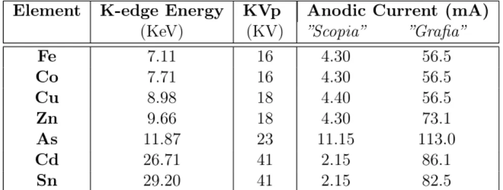
Is possible to choose between different current position, from 1 to 6, but an effective monitoring of current value is provided by power supply monitor. Some typical KVp and anodic current used for imaging and spectral measurement are reported in table 2.1.
2.2 Mosaic crystal 19
Element K-edge Energy KVp Anodic Current (mA)
(KeV) (KV) ”Scopia” ”Grafia”
Fe 7.11 16 4.30 56.5 Co 7.71 16 4.30 56.5 Cu 8.98 18 4.40 56.5 Zn 9.66 18 4.30 73.1 As 11.87 23 11.15 113.0 Cd 26.71 41 2.15 86.1 Sn 29.20 41 2.15 82.5
Table 2.1: Some typical working condition for spectrum and imaging analysis
2.2 Mosaic crystal
The bremsstrahlung beam is monochromatized by a highly oriented pyrolytic graphite mosaic crystal (HOPG)3, 60×28mm2 wide and 1mm thick with nominal a mosaic spread
of 0.28°.
2.3 Optical bench
The imaging system is presented in Fig.2.1.
The X-ray tube is mounted on an arm fixed to a motorized goniometer Microcontrole4
rotating with an accuracy of 0.001° from 0° to a maximum angle of 2θ=90°.
The mosaic crystal is placed 250 mm away from the X-ray focal spot on a motorized tilt/linear stage in order to enable optimal alignment of the apparatus. The system is mounted on another isocentric goniometer that can rotate with an accuracy of 0.001° to a maximum angle of θ=45°.
This set-up provides a monochromatic beam always perpendicular to the imaging plane independently of the tuned X-ray energy. The monochromatic beam, at a 250 mm distance from the crystal is collimated by a 8 mm wide lead slit.
A motorized scanning system is placed 350 mm downstream the first collimator and is used as a support for the painting, which can be scanned by this automated system. A second motorized scanning system is placed 240 mm away from the first (1090 mm distance from the X-ray focal spot) and is the support for the detectors. All the scanning systems and goniometers are connected to a multi axis motion controller unit 5.
3Optigraph Ltd, Moscow, Russia
4Microcontrole, Evry, France; now Newport, USA
20 Experimental apparatus
2.4 Detectors
Three different detectors have been used to perform spectrum analysis and K-edge elemental mapping.
• Spectrum analysis
To perform spectral analysis a cadmium zinc telluride detector (CZT) was used. XR-100T-CZT 6 is a solid-state detector with 25mm2 area, 2 mm thickness, 250
µm beryllium window and a resolution of 900 eV FWHM at 59 KeV .
Within the energy range considered in this work, 7-40 KeV, the efficiency of the CZT detector is approximately 100% [18].
In order to reduce the X-ray photon fluxes on the detector a pinhole with a diameter of 224 µm has been used.
• Imaging
Two silicon detectors have been used to perform a comparison of element recognition of different imaging detectors: a commercial Charged Coupled Device, CCD S71997,
and a Silicon Strip Detector (SSD) realized by FBK8 on a design by the Department
of Science and Advanced Technology of Piemonte Orientale University. – CCD
The Hamamatsu CCD is a FFT (Front-Illuminated) detector without FOS (Fiber Optic plate with Scintillator).
The CCD has a nominal thickness of 300 µm, a total active area of 3072×128 pixels (two different CCD chips, 1536×128 pixels) and 48µm pixel size which allows a good spatial resolution.
The first layer of FOS, the scintillator, converts high energy photons to visible light and fiber optics allow a high efficient photon transport to the CCD surface. This type of structure prevents radiation damage on Silicon surface by stopping high energy photons reaching the bulk.
However the FOS layer presents two significant defects: on one hand resolution get worst due to non direct detection on the Silicon surface. On other hand low energy X-ray photons are converted on the first layer of scintillator surface so visible photons don’t reach the Silicon active area, making the efficiency lower. To improve efficiency at low energy and spatial resolution a CCD without FOS has been chosen.
This choose, like illustrate in chapter 3, has let to a radiation damage. CCD electronics allows to set gain and offset for the two detectors indepen-dently to obtain an homogeneous signal [19].
6Amptek inc., MA, USA
7Hamamatsu Photonics K.K., Japan
2.4 Detectors 21 – SSD
The SSD has been realized with 512 Si-strip, 1 cm thick and 300×100 µm pixel size. It is a Edge-on detector and it works in single photon counting mode [20]. Edge-on configuration allows a major penetration thickness to increase effi-ciency in the 20-40 KeV energy range. To ensure a very small dead area of the SSD working in this configuration, the detector is cut perpendicular to the strips at a distance of only 20 µm from the end of the strips.
The SSD electronics allows to perform a calibration for each single strip to obtain a homogeneous response along 512 strips. It is also possible to set two different energy thresholds to acquire independent signals at two different energies.
Chapter 3
Radiation damage on CCDs
In solid state detector high radiation dose may cause radiation damage. Different types of effects can occur: defect on charge transfer, high dark current, ghost images are often observe.
In the following section CCD structure, working principle and radiation damage will be discussed.
3.1 Charge Coupled Device
Usually this types of detectors are used as imaging detectors, integrating all interacting photons. Depending on the read-out electronics, counting mode is also possible.
When photons interacts with semiconductor layer electron-hole pairs are generated pro-portionally to the energy of the incident photons. The generated charge is stored in each pixel and sequentially transferred from adjacent pixels and read-out at the end of the pixel line, as illustrated in next section.
3.1.1 Structure
Figure 3.1, from [21], show the section of a Front Illuminated, Two-Phase CCD, based upon a MOS (Metal Oxide Semiconductor) capacitor.
Front illuminated CCD (FI-CCD) identify detectors that receive and detect light form the front side, where electrodes are positioned.
Two phase signals are applied to two metal electrodes (P1, P2) for each pixel used to transfer charge.
Fig.3.1[a] shown a two phase CCD structure, based on non-conductive oxide layer, a Silicon Dioxide layer SiO2 and semiconductor channel of Si is present as base layer.
When a voltage is applied to the gates (P1 and P2) a depletion zone, with a thickness of few microns, is created.
Thanks to the potential applied during the integration period charge generated by photons interaction is stored in the potential well region in the photosensitive section.
24 Radiation damage on CCDs
[a] [b]
Figure 3.1: CCD structure, from [21]
By applying two clock pulses with different voltage levels to the electrodes charge is sequentially transferred from pixel to pixel.
Read-out is controlled by the CCD register, composed of three different sections, as shown in Fig.3.1[b].
The Vertical register are the photosensitive pixels, grouped in columns (in our detector 128), which carried out collected charge at the end of the columns. The Horizontal register collect this signals and transfer charges to Chip amplifier. The Chip amplifier convert the charge derived from Horizontal register to a voltage signal.
3.2 Optimization of the system
For CCD imagers there are three major sources of dark current, i.e charge generation with no incident light.
• Thermal generation and diffusion in neutral bulk region • Thermal generation in depletion zone
• Thermal generation due to surface state at Si − SiO2 interface
Of these sources, the contribution from interface states is the dominant contributor of dark current for multi-phase CCDs [21].
Since either case is associated with heat or temperature, the dark current has a strong correlation with temperature.
To obtain a good signal-to-noise ratio is necessary to minimize dark current. Two methods are presented in the following to achieve that aim: cooling and optimization of the gate’s voltage.
3.2.1 Cooling
As mentioned above dark current is correlated with device temperature. For CCD used it doubles for every 5 to 7°C increase in temperature [21]. A cooling system is usually realized with a Peltier cell under or behind detector.
3.2 Optimization of the system 25 2000 1800 1600 1400 1200 1000 800 600
Dark Current ( Gray Level )
26 24 22 20 18 16 Temperature ( °C )
Figure 3.2: Measured dark current as average gray level vs. detector temperature
Our detection system present a double Peltier cell under CCD, one for every part of the detector.
A cooling test has been realized acquiring dark images at different temperatures. As illustrated in figure 3.2 the dark current, evaluated by average gray levels in the CCD image, is decreasing as temperature decreases.
Unfortunately at present our custom electronics does not support a permanent cooling system: it is not sealed and humidity deposition on electronics is unavoidable. This cooling system has not been used.
3.2.2 Optimization of the gate voltage
As mentioned above the contribution from interface states (from Si and SiO2) is the
dominant contributor of dark current for multi-phase CCDs.
Dark current generation at this interface depends on two factors, namely the density of interface states and the density of free carriers (holes and electrons) that populate the interface [22].
Electrons that thermally “hop“ from the valence band to an interface state (sometimes referred to as a mid-band state) and to the conduction band produce a dark e-h pair. The presence of free carriers will fill interface states and, if the states are completely populated, will suppress hopping and conduction and substantially reduce dark current to the bulk dark level.
In MPP technology, Multi Pinned Phase, also referred as inverted operation, dark current is significantly curtailed by inverting the signal carrying channel by populating the Si-SiO2 interface with holes which, as mentioned above, suppresses the hopping conduction
process [22].
For pinning to occur, the gate voltage is made increasingly more negative. At certain negative gate voltage the valence band at the Si-SiO2 interface reaches the potential of
the valence band in the bulk semiconductor.
If substrate is grounded, the holes from that channel stop region ”pin” the valence band to ground and no additional charge in channel potential occur. The voltage at which this occur is called the pinning gate voltage.
This is implemented by setting all MOS gate to the inverted state [21].
26 Radiation damage on CCDs ion implantation between the collecting and the barrier phase.
This means the CCD still provides the potential well even when all the gate are set to the same voltage. MPP operation is then performed applying a bias so all phases of the CCD are set to the inverted state.
This inversion cause the conduction proprieties of the semiconductor to change from P-type semiconductor to N-type or vice-versa.
As shown in the potential distribution in figure 3.3, from [21], both the collecting and barrier phase are pinned in the inverted state. In the pinning state the CCD surface is inverted by holes supplied from the channel stop region. The potential at Si-SiO2
interface is pinned and fixed at the same potential as the substrate, even if a further negative voltage is applied [21].
Figure 3.3: Potential schematization in MPP, from [21]
In this state while inverted by hole, thermally generated electrons at Si-SiO2 interface
can be dramatically suppressed, thus achieving a very low dark current.
In MPP operation is important to apply an optimum pinning voltage since the greatly affects the dark current characteristics. As illustrated in figure 3.4[a], from [21], the dark output cannot be reduced to a minimum level because the inverted layer is not fully formed by holes.
To optimize our system a study of optimum pinning voltage has been achieved. Our custom electronics allows to control the two gate voltage separately and so interact directly with voltage setting.
Has been measured dark current with 2 seconds of exposition time without X-ray and changing gates voltage. As shown in figure 3.4[b] dark current has been decreased setting gate voltage below -8 V.
3.3 Radiation Damage 27 [a] [b] 2600 2400 2200 2000 1800 1600
Dark CUrrent ( Gray Level )
-12 -11 -10 -9 -8 -7 -6 Gate Voltage ( V )
Figure 3.4: Decrease of dark current decreasing gate voltage: [a] from [21] and [b] result obtained on CCD S7199.
3.3 Radiation Damage
Radiation effects on CCD detector can be various and two major classes can be identified.
First are cumulative effects derive from total ionizing dose (TID) and displace damage and second classified as single event effects (SEE).
Working with low energetic photons while cumulative effect derived from TID can occur, displace damage or single event effects cannot.
In general TDI damage interest the oxide and the bulk-oxide interface through ionization. This form of damage results in changes in the flat band voltage, increased surface dark current and changes in linearity.
• Flat Band Shift
Ionization-induced damage induces a build-up of charge in the CCD’s gate insulator causing a change in the flat band voltage namely flat-band shift.
Analyzing our CCD detector a change in the flat band voltage has been found out and, working as explain above, effect of increased surface dark current derived from shift in the flat band voltage has been alleviated by re-setting a new optimized gate voltage (view 3.4 [b]).
• Dark current
In addition electrons traps has been created by radiation damage at the silicon-silicon dioxide interface which slowly de-trap into the pixel’s potential well causing the CCD’s dark current to increase.
Figures 3.5 and 3.6 shown radiation damage suffered by CCD detector after 2 working year and approximately a total flux of 6·109 photons/mm2 in energy range
9 - 10keV .
Images in Fig.3.5 are acquired with the same time exposition, reported in a 8-bit grayscale and shown with the same contrast and luminosity to obtain a correct results interpretation. Fig. 3.5[a] is the image obtained with a new CCD, never
28 Radiation damage on CCDs [a] !
[b] !
[c] [d]
Figure 3.5: Comparison between images and histograms of the new CCD [a,c] and the CCD with radiation damage [b,d] with same exposition time.
2000 1800 1600 1400 1200 1000 800 600 400 200 0
Dark Current ( Gray Level )
14 13 12 11 10 9 8 7 6 5 4 3 2 1 0 Exposition time ( s )
Mean dark current value of New CCD Mean dark current value on damage CCD after 2 years exposition
Figure 3.6: Plot of increasing of dark current effect after radiation damage
exposed to X-rays, and 3.5[b] the same CCD after two working years with X-rays. Histograms of the images are presented in Fig. 3.5[c,d].
Analyzing this comparison dark current increase is evident on all CCD surface and some residual images are visible. This is due to a non homogeneous dose suffered by detector and consequently a non-homogeneous radiation damage.
Plot in Fig. 3.6 represent mean gray level value on all CCD surface for different time exposition, for the CCDs new and damaged.
3.3 Radiation Damage 29 [a] 400 350 300 250 200 150 100
Mean Gray level
100 80 60 40 20 0 Pixels Column CCD A : 1sec 2sec 3sec 4sec 5sec [b] 400 350 300 250 200 150 100 100 80 60 40 20 0 CCD B : 1sec 2sec 3sec 4sec 5sec [c] 300 250 200 150 100 50 0 Gray level 5 4 3 2 1 0
Exposition time (sec)
CCD A [d] 300 250 200 150 100 50 0 Gray level 5 4 3 2 1 0
Exposition time (sec)
CCD B
Figure 3.7: Changes in linearity with radiation damage
• Changes in linearity
Images at same energy, 10 KeV, same anode current and increasing exposition time, from 1 to 5 seconds, have been taken. In Fig. 3.7[a,b] the plot of mean column values, shown separated for the two different part of detector, namely CCD A and CCD B, is shown. The same result, as mean gray levels obtain vs. exposition time, is shown in Fig. 3.7[c,d].
As expected different behavior of the two detectors is highlighted and a not linear response to X-ray intensity increased is shown. In this working condition a white field correction and Lehmann algorithm does not work correctly.
Chapter 4
Characterization of the X-ray
source
With our facility 7-40 KeV energy range has been investigated where K-edge of more elements that characterize pigments are located, as illustrated 1.5.
4.1 Measurement setting
CZT detector has been used to perform spectrum analysis of the source in different KVp and energy conditions.
All measurement have been performed positioning detector on the last motorized system at 1090 cm from the focus of the tube.
Deriving from the many degrees of freedom of the system a not perfect alignment from goniometers and crystal entails a slight deviation of the center of monochro-matic beams from the geometrical center on imaging plane.
It has been taken into account finding the center of monochromatic beams identified as the maximum signal position.
A small lead collimator, with 224 ± 13µm diameter, has been used in front of CZT detector.
Further, an analysis was performed to determine detector energy resolution in our energy range. The nominal energy resolution is explicitly indicated by datasheet only for 59.5 KeV Am241 peak energy.
Beam energy has been set at K-edge energy of Iron, Cobalt, Copper, Zinc, Arsenic, Bromine, Strontium, Molybdenum, Silver, Cadmium, Tin and Barium.
In order to characterize quasi-monochromatic spectra, an analysis has been realized at the K-edge beam energies; also slightly lower energy (E−) and slightly higher
energy (E+) have been analyzed.
The choice of energy “low“ and “high“ was done as a compromise between the two competing requirements of having lower energy difference from Low and High energy beams and of the minimum superposition of the spectra. For energy beams from up to Bromine K-edge (13.47 KeV) an energy distance of 1.3 KeV between high and low beams was chosen.
32 Characterization of the X-ray source At higher energy more spacing was necessary due to the spread of monochromatized beams.
Bremsstrahlung spectrum of the source has been analyzed at the same KVp con-dition of monochromatic beams to calculate monochromatization efficiency of the crystal.
Integrated reflectivity has been calculated by compared photon flux of continuous and monochromatized beam in the same energy range, related to crystal spread. Let θ the Bragg angle and ω the mosaic spread of the crystal, diffracted beam has a narrow energy band related the angle range
θ + ω < θ < θ− ω.
Photons in this energy range, Eθ−ω < Eθ < Eθ+ω, have been considered for
monochromatization efficiency.
All results are presented in term of normalized total flux, photon/mAs · mm2.
4.2 CZT energy resolution
In order to perform a complete characterization of the system, a preliminary mea-surement has been done to measure effective energy resolution of the CZT detector. Two reference sources, Am241 and Co57, have been analyzed.
Resulting peak widths have been calculated and the energy resolution found is shown in Fig 4.1.
4.3 Iron K-edge: 7.11 KeV 33
4.3 Iron K-edge: 7.11 KeV
To realize analysis at Iron K-edge energy would be necessary to set KVp to prevent the second order diffraction. Unfortunately our system does not allows to set a KVp lower than 16KV and second harmonic has been generated.
In Fig 4.2 a comparison between continuos beam and monochromatic beam at Iron K-edge energy (7.11 KeV), both setting KVp at 16KV, is show.
Fig.4.3 shown quasi-monochromatic spectra obtained at slightly lower energy (E−
6.46 KeV) and slightly higher energy (E+ 7.76 KeV).
As explain above, set of KVp has generated second order diffraction beam. Its has been product only for the lower energy beam and its peaked on 13KeV.
However, by using a SSD this can be eliminated by threshold setting. With our traditional CCD this energy configuration to investigate Iron cannot be used. Monochromatization efficiency has been calculated by compared photon flux of continuous and monochromatized beam in the energy range related to crystal spread. Only first diffraction order has been take in account. Only a small fraction of the beam (15.2%) has been monochromatized.
In Fig 4.4 are present monochromatic spectrum with only first diffraction order and residuals relative to the gaussian fit.
Table 4.13 show energy beam set, peak position, energy resolution and total photon flux of the beam.
Setting diffraction angle to obtain Fe K-edge energy, 7.11 KeV, energy peak of 7.18 KeV is obtained.
This slight deviation depends on the mechanical misalignment.
300 250 200 150 100 50 0
Number of Photons (photons/mA*s*mm
2 ) 16 14 12 10 8 6 4 2 0 Energy (KeV)
Monochromatic spectrum at Fe K-edge energy and 16 KV continuous spectrum at the same conditions Continuous spectrum Fe K-edge energy 7.11 KeV
34 Characterization of the X-ray source 35 30 25 20 15 10 5 0
Number of Photons (photons/mA*s*mm
2 ) 16 14 12 10 8 6 4 2 0 Energy (KeV)
Monochromatic spectrum near Fe K-edge energy Fe Low energy 6.46 KeV Fe High energy 7.76 KeV
Figure 4.3: Fe: First and second order diffraction of Fe
[a] 35 30 25 20 15 10 5 0
Number of Photons (photons/mA*s*mm
2 ) 12 10 8 6 4 2 Energy (KeV)
Monochromatic spectrum near Fe K-edge energy Fe Low energy 6.46 KeV Fe High energy 7.76 KeV
[b] -4 -3 -2 -1 0 1 2 3 4 12 10 8 6 4 2 Fe
Figure 4.4: Fe: [a] monochromatic beam on energies bracketing K-edge energy and [b] residuals relative to the gaussian fit
4.4 Cobalt K-edge: 7.71 KeV 35
Fe Setting Energy x0 FWHM Flux
KeV KeV KeV ph/mm2∗ mA ∗ s
K-edge 7.11 7.18 0.47 115 ±11
Low 6.46 6.54 0.34 56 ±7
High 7.76 7.92 0.38 211 ±15
Table 4.1: Characteristics of the diffracted beams on Iron K-edge energy.
4.4 Cobalt K-edge: 7.71 KeV
At Cobalt K-edge energy the same KVp of Iron measures has been set.
Fig. 4.5 show a comparison between continuos and monochromatic beam at Cobalt K-edge energy, both setting KVp at 16KV.
A slightly increased energy photon flux at this higher energy is found: 212 ± 15ph/mm2· mA · s at K-edge energy and a monochromatization efficiency of 17.7% is found.
In Fig. 4.6 are present monochromatic spectrum and residuals relative to gaussian fit; table 4.2 show spectra data obtained.
350 300 250 200 150 100 50 0
Number of Photons (photons/mA*s*mm
2 ) 16 14 12 10 8 6 4 2 0 Energy (KeV)
Monochromatic spectrum at Co K-edge energy and 16 KV continuous spectrum at the same conditions Continuous spectrum Co K-edge energy 7.71 KeV
Figure 4.5: Co: Bremsstrahlung spectrum at 16 KVp and monochromatic beam on K-edge energy
36 Characterization of the X-ray source [a] 50 40 30 20 10 0
Number of Photons (photons/mA*s*mm
2 ) 12 10 8 6 4 Energy (KeV)
Monochromatic spectrum near Co K-edge energy Co Low 7.06 KeV Co High 8.36 KeV [b] -10 -5 0 5 10 12 10 8 6 4 Co
Figure 4.6: Co: [a] monochromatic beam on energies bracketing K-edge energy and [b] residuals relative to the gaussian fit
Co Setting Energy x0 FWHM Flux
KeV KeV KeV ph/mm2∗ mA ∗ s
K-edge 7.71 7.91 0.42 212 ±15
Low 7.06 7.26 0.46 99 ±10
High 8.36 8.51 0.46 333 ±18
4.5 Copper K-edge: 8.98 KeV 37
4.5 Copper K-edge: 8.98 KeV
For the Copper K-edge spectrum an increased value of KVp at 18 KV has been used.
As shown in Fig. 4.8 and reported in table 4.3 a KVp increasing correspond to a photon flux increase and at 9.17 KeV flux of 600 ± 24ph/mm2· mA · s is obtained.
In this case a monochromatization efficiency of 22.3% is found.
400
300
200
100
0
Number of Photons (photons/mA*s*mm
2 ) 20 18 16 14 12 10 8 6 4 2 0 Energy (KeV)
Monochromatic spectrum at Cu K-edge energy and 18kV continuous spectrum at the same conditions Continuous spectrum Cu K-edge energy 8.98 KeV
Figure 4.7: Cu: Bremsstrahlung spectrum at 18 KVp and monochromatic beam on K-edge energy
Cu Setting Energy x0 FWHM Flux
KeV KeV KeV ph/mm2∗ mA ∗ s
K-edge 8.98 9.17 0.40 600 ±24
Low 8.33 8.48 0.33 497 ±22
High 9.63 9.82 0.40 781 ±28
38 Characterization of the X-ray source [a] 120 100 80 60 40 20 0
Number of Photons (photons/mA*s*mm
2 ) 14 12 10 8 6 4 Energy (KeV)
Monochromatic spectrum near Cu K-edge energy Cu Low 8.33 KeV Cu High 9.63 KeV [b] -6 -4 -2 0 2 4 6 14 12 10 8 6 4 Cu
Figure 4.8: Cu: [a] monochromatic beam on energies bracketing K-edge energy and [b] residuals relative to the gaussian fit
4.6 Zinc K-edge: 9.66 KeV
To perform spectrum analysis at Zinc energies is used a KVp of 20 KV and a monochromatization efficiency of 30.7% is obtained.
As shown in Fig. 4.10 and reported in table 4.4 increasing energy beams increase slightly deviation of the energy beams, in this case about 0.2 KeV; beams energy of 9.87 KeV, 9.26 KeV and 10.52 KeV are obtained.
4.6 Zinc K-edge: 9.66 KeV 39 400 350 300 250 200 150 100 50 0
Number of Photons (photons/mA*s*mm
2 ) 20 15 10 5 0 Energy (KeV)
Monochromatic spectrum at Zn K-edge energy and 20 KV continuous spectrum at the same conditions Continuous spectrum Zn K-edge energy 9.66 KeV
Figure 4.9: Zn: Bremsstrahlung spectrum at 20 KVp and monochromatic beam on K-edge energy [a] 140 120 100 80 60 40 20 0
Number of Photons (photons/mA*s*mm
2 ) 14 12 10 8 6 Energy (KeV)
Monochromatic spectrum near Zn K-edge energy Zn Low 9.00 KeV Zn High 10.30 KeV [b] -8 -6 -4 -2 0 2 4 6 8 14 12 10 8 6 Zn
Figure 4.10: Zn: [a] monochromatic beam on energies bracketing K-edge energy and [b] residuals relative to the gaussian fit
40 Characterization of the X-ray source
Zn Setting Energy x0 FWHM Flux
KeV KeV KeV ph/mm2∗ mA ∗ s
K-edge 9.66 9.87 0.42 940 ±31
Low 9.00 9.26 0.42 708 ±27
High 10.30 10.52 0.40 1098 ±33
Table 4.4: Characteristics of the diffracted beams on Zinc K-edge energy.
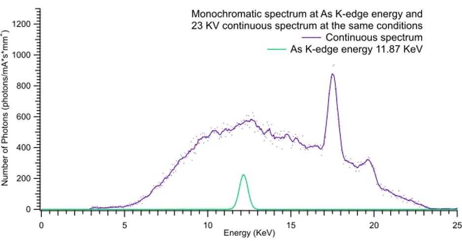
4.7 Arsenic K-edge: 11.87 KeV
To perform measure at Arsenic energy has been used 23 KV.
In Fig.4.11 are shown Bremsstrahlung spectrum of the source and monochromatic spectrum at As K-edge energy. At this KVp emission peaks of the Molybdenum anode are observable in the continuous beam, Kα=17.48 KeV and Kβ=19.61 KeV.
Quasi-monochromatic beams and photon flux obtained are shown in Fig. 4.12 and reported in table 4.5 respectively.
Monochromatization efficiency of 26.7% is obtained.
1200 1000 800 600 400 200 0
Number of Photons (photons/mA*s*mm
2 ) 25 20 15 10 5 0 Energy (KeV)
Monochromatic spectrum at As K-edge energy and 23 KV continuous spectrum at the same conditions Continuous spectrum As K-edge energy 11.87 KeV
Figure 4.11: As: Bremsstrahlung spectrum at 23 KVp and monochromatic beam on K-edge energy
4.7 Arsenic K-edge: 11.87 KeV 41 [a] 300 250 200 150 100 50 0
Number of Photons (photons/mA*s*mm
2 ) 16 14 12 10 8 6 Energy (KeV)
Monochromatic spectrum near As K-edge energy As Low 11.22 KeV As High 12.52 KeV [b] -10 -8 -6 -4 -2 0 2 4 6 8 10 16 14 12 10 8 6 As
Figure 4.12: As: [a] monochromatic beam on energies bracketing K-edge energy and [b] residuals relative to the gaussian fit
As Setting Energy x0 FWHM Flux
KeV KeV KeV ph/mm2∗ mA ∗ s
K-edge 11.87 12.16 0.43 2307 ±48
Low 11.22 11.48 0.38 2085 ±46
High 12.52 12.90 0.45 2522 ±50
42 Characterization of the X-ray source
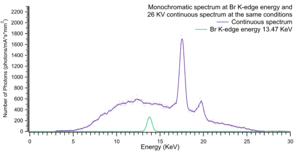
4.8 Bromine K-edge: 13.79 KeV
Measurement on Bromine K-edge energy has been realized with 26 KVp. Quasi-monochromatic beams and photon flux obtained are shown in Fig. 4.14 and reported in table 4.6 respectively.
Monochromatization efficiency of 32.5% is obtained.
2200 2000 1800 1600 1400 1200 1000 800 600 400 200 0
Number of Photons (photons/mA*s*mm
2 ) 30 25 20 15 10 5 0 Energy (KeV)
Monochromatic spectrum at Br K-edge energy and 26 KV continuous spectrum at the same conditions Continuous spectrum Br K-edge energy 13.47 KeV
Figure 4.13: Br: Bremsstrahlung spectrum at 26 KVp and monochromatic beam on K-edge energy
Br Setting Energy x0 FWHM Flux
KeV KeV KeV ph/mm2∗ mA ∗ s
K-edge 13.47 13.78 0.47 3003 ±55
Low 12.82 13.09 0.46 3147 ±56
High 14.12 14.38 0.46 3134 ±56
4.9 Strontium K-edge: 16.20 KeV 43 [a] 500 450 400 350 300 250 200 150 100 50 0
Number of Photons (photons/mA*s*mm
2 ) 18 16 14 12 10 8 Energy (KeV)
Monochromatic spectrum near Br K-edge energy Br Low 12.82 KeV Br High 14.12 KeV [b] -20 -10 0 10 20 18 16 14 12 10 8 Br
Figure 4.14: Br: [a] monochromatic beam on energies bracketing K-edge energy and [b] residuals relative to the gaussian fit
4.9 Strontium K-edge: 16.20 KeV
Measurement on Strontium K-edge energy has been realized with 31 KVp.
An increase energy distance between monochromatic beams energy is used to prevent beams overlap. Low and high spectra have been acquired at E−=15.2 KeV and
E+= 17.20 KeV.
In Fig. 4.15 are shown monochromatic beams. As also reported in 4.8 a great photon flux disparity from the low and high energy beams is identified.
This is due by the influence of the Kα emission peak of the Mo anode at 17.40 KeV.
44 Characterization of the X-ray source 6000 5000 4000 3000 2000 1000 0
Number of Photons (photons/mA*s*mm
2 ) 35 30 25 20 15 10 5 0 Energy (KeV)
Monochromatic spectrum at Sr K-edge energy and 31 KV continuous spectrum at the same conditions Continuous spectrum Sr K-edge energy 16.20 KeV
Figure 4.15: Sr: Bremsstrahlung spectrum at 31 KVp and monochromatic beam on K-edge energy [a] 1000 900 800 700 600 500 400 300 200 100 0
Number of Photons (photons/mA*s*mm
2 ) 22 20 18 16 14 12 Energy (KeV)
Monochromatic spectrum near Sr K-edge energy Sr Low 15.20 KeV Sr High 17.20 KeV [b] -40 -20 0 20 40 22 20 18 16 14 12 Sr
Figure 4.16: Sr: [a] monochromatic beam on energies bracketing K-edge energy and [b] residuals relative to the gaussian fit
4.10 Molybdenum K-edge: 19.99 KeV 45
Sr Setting Energy x0 FWHM Flux
KeV KeV KeV ph/mm2∗ mA ∗ s
K-edge 16.20 16.40 0.53 2819 ±53
Low 15.20 15.37 0.47 957 ±31
High 17.20 17.53 0.45 8927 ±94
Table 4.7: Characteristics of the diffracted beams on Strontium K-edge energy.
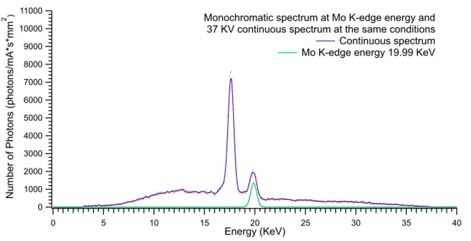
4.10 Molybdenum K-edge: 19.99 KeV
At this energy, obtained with 36 KVp, Kβ peak influence on monochromatic beam
is massive.
Monochromatic beams at K-edge energy, 19.99 KeV, has almost the same energy of Kβ anode emission, 19.61 KeV.
As shown in Fig 4.18 and reported in table 4.8 that comport a much higher photon flux, 16306 ±127ph/mm2· mA · s, compared with flux at low and high energy, 6153
±78 and 3433 ±59ph/mm2· mA · s respectively.
At this energies spread of the beams, about 0.51 KeV, made necessary an energy separation increase, 2 KeV.
Monochromatization efficiency of 42.7% is obtained.
11000 10000 9000 8000 7000 6000 5000 4000 3000 2000 1000 0
Number of Photons (photons/mA*s*mm
2 ) 40 35 30 25 20 15 10 5 0 Energy (KeV)
Monochromatic spectrum at Mo K-edge energy and 37 KV continuous spectrum at the same conditions Continuous spectrum Mo K-edge energy 19.99 KeV
Figure 4.17: Mo: Bremsstrahlung spectrum at 36 KVp and monochromatic beam on K-edge energy
46 Characterization of the X-ray source [a] 500 400 300 200 100 0
Number of Photons (photons/mA*s*mm
2 ) 24 22 20 18 16 Energy (KeV)
Monochromatic spectrum near Mo K-edge energy Mo Low 17.99 KeV Mo High 21.99 KeV [b] 60 40 20 0 -20 -40 -60 24 22 20 18 16 Mo
Figure 4.18: Mo: [a] monochromatic beam on energies bracketing K-edge energy and [b] residuals relative to the gaussian fit
Mo Setting Energy x0 FWHM Flux
KeV KeV KeV ph/mm2∗ mA ∗ s
K-edge 19.99 19.87 0.51 16306 ±127
Low 17.99 18.26 0.64 6153 ±78
High 21.99 22.31 0.66 3433 ±59
4.11 Silver K-edge: 25.51 KeV 47
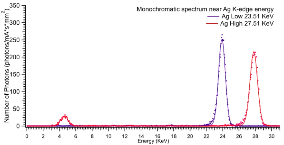
4.11 Silver K-edge: 25.51 KeV
To realize measurement on Silver K-edge energy has been used maximum KVp achievable, 41 KVp.
As shown in Fig. 4.21 and reported in table 4.9 at this energies low energy beam present an higher flux than high energy, 4259 ±65 and 4075 ±64ph/mm2· mA · s
respectively.
Analyzing obtained spectrum (Fig. 4.20) a noise peaked in 4-5 KeV range is observed.
With traditional CCD this part of the flux cannot be delate. However by using a SSD this portion of the spectra can eliminated by threshold setting.
Monochromatization efficiency at this energy is 16.5%.
14000 12000 10000 8000 6000 4000 2000 0
Number of Photons (photons/mA*s*mm
2 ) 40 30 20 10 0 Energy (KeV)
Monochromatic spectrum at Ag K-edge energy and 41 KV continuous spectrum at the same conditions Continuous spectrum Ag K-edge energy 25.51 KeV
Figure 4.19: Ag: Bremsstrahlung spectrum at 41 KVp and monochromatic beam on K-edge energy 350 300 250 200 150 100 50 0
Number of Photons (photons/mA*s*mm
2 ) 30 28 26 24 22 20 18 16 14 12 10 8 6 4 2 0 Energy (KeV)
Monochromatic spectrum near Ag K-edge energy Ag Low 23.51 KeV Ag High 27.51 KeV
48 Characterization of the X-ray source [a] 350 300 250 200 150 100 50 0
Number of Photons (photons/mA*s*mm
2 ) 30 28 26 24 22 Energy (KeV)
Monochromatic spectrum near Ag K-edge energy Ag Low 23.51 KeV Ag High 27.51 KeV [b] -40 -30 -20 -10 0 10 20 30 40 30 28 26 24 22 Ag
Figure 4.21: Ag: [a] monochromatic beam on energies bracketing K-edge energy and [b] residuals relative to the gaussian fit
Ag Setting Energy x0 FWHM Flux
KeV KeV KeV ph/mm2∗ mA ∗ s
K-edge 25.51 25.93 0.79 4085 ±64
Low 23.51 23.91 0.70 4259 ±65
High 27.51 27.80 0.78 4075 ±64
4.12 Cadmium K-edge: 26.71 KeV 49
4.12 Cadmium K-edge: 26.71 KeV
To realize measurement on Cadmium K-edge energy has been used 41 KVp. As shown in Fig 4.23 also in this analysis the noise is observed. Monochromatic beams and photon flux obtained are shown in Fig. 4.24 and reported in table 4.10. Monochromatization efficiency of 14.8% is observed.
11000 10000 9000 8000 7000 6000 5000 4000 3000 2000 1000 0
Number of Photons (photons/mA*s*mm
2 ) 40 30 20 10 0 Energy (KeV)
Monochromatic spectrum at Cd K-edge energy and 41 KV continuous spectrum at the same conditions Continuous spectrum Cd K-edge energy 26.71 KeV
Figure 4.22: Cd: Bremsstrahlung spectrum at 41 KVp and monochromatic beam on K-edge energy. 300 250 200 150 100 50 0
Number of Photons (photons/mA*s*mm
2 ) 30 28 26 24 22 20 18 16 14 12 10 8 6 4 2 0 Energy (KeV)
Monochromatic spectrum near Cd K-edge energy Cd Low 24.71 KeV Cd High 28.71 KeV
50 Characterization of the X-ray source [a] 300 250 200 150 100 50 0
Number of Photons (photons/mA*s*mm
2 ) 30 28 26 24 22 Energy (KeV)
Monochromatic spectrum near Cd K-edge energy Cd Low 24.71 KeV Cd High 28.71 KeV [b] -40 -20 0 20 40 30 28 26 24 22 Cd
Figure 4.24: Cd: [a] monochromatic beam on energies bracketing K-edge energy and [b] residuals relative to the gaussian fit
Cd Setting Energy x0 FWHM Flux
KeV KeV KeV ph/mm2∗ mA ∗ s
K-edge 26.71 27.38 0.80 4163 ±65
Low 24.71 24.81 0.77 4205 ±65
High 28.71 28.85 0.88 4117 ±64
4.13 Tin K-edge: 29.20 KeV 51
4.13 Tin K-edge: 29.20 KeV
Also to realize measurement on Tin K-edge energy has been used 41 KVp and, as is shown in Fig.4.26, the low energy noise is observed.
Monochromatic beams and photon flux obtained are shown in Fig. 4.27 and reported in table 4.11.
Monochromatization efficiency of 3.2% is obtained.
14000 12000 10000 8000 6000 4000 2000 0
Number of Photons (photons/mA*s*mm
2 ) 40 35 30 25 20 15 10 5 0 Energy (KeV)
Monochromatic spectrum at Sn K-edge energy and 41 KV continuous spectrum at the same conditions Continuous spectrum Sn K-edge energy 29.20 KeV
Figure 4.25: Sn: Bremsstrahlung spectrum at 41 KVp and monochromatic beam on K-edge energy 50 40 30 20 10 0
Number of Photons (photons/mA*s*mm
2 ) 40 35 30 25 20 15 10 5 0 Energy (KeV)
Monochromatic spectrum near Sn K-edge energy Sn Low 27.20 KeV Sn High 31.20 KeV
52 Characterization of the X-ray source [a] 50 40 30 20 10 0
Number of Photons (photons/mA*s*mm
2 ) 34 32 30 28 26 24 Energy (KeV)
Monochromatic spectrum near Sn K-edge energy Sn Low 27.20 KeV Sn High 31.20 KeV [b] -10 -5 0 5 10 34 32 30 28 26 24 Sn
Figure 4.27: Sn: [a] monochromatic beam on energies bracketing K-edge energy and [b] residuals relative to the gaussian fit
Sn Setting Energy x0 FWHM Flux
KeV KeV KeV ph/mm2∗ mA ∗ s
K-edge 29.20 29.07 0.88 818 ±29
Low 27.20 27.00 0.80 781 ±28
High 31.20 30.70 0.98 783 ±28
4.14 Barium K-edge: 37.44 KeV 53
4.14 Barium K-edge: 37.44 KeV
To realize measurement on Barium K-edge energy has been used 41 KVp. As shown in Fig.4.26 Bremsstrahlung shape is recognizable, probably due to a non-perfect collimation of the source.
At this energy Bragg diffraction requires small angles and a fraction of the primary beam impinging on the detector. Emission peaks of the source are distinguishable. To perform K-edge radiography on Barium CCD is not usable and SSD became indispensable.
Monochromatic beams and photon flux obtained are shown in Fig. 4.30 and reported in table 4.12.
At this energy monochromatization efficiency of 2.5% is obtained.
14000 12000 10000 8000 6000 4000 2000 0
Number of Photons (photons/mA*s*mm
2 ) 40 35 30 25 20 15 10 5 0 Energy (KeV)
Monochromatic spectrum at Ba K-edge energy and 41 KV continuous spectrum at the same conditions Continuous spectrum Ba K-edge energy 37.44 KeV
Figure 4.28: Ba: Bremsstrahlung spectrum at 41 KVp and monochromatic beam on K-edge energy 30 25 20 15 10 5 0
Number of Photons (photons/mA*s*mm
2 ) 40 35 30 25 20 15 10 5 0 Energy (KeV)
Monochromatic spectrum near Ba K-edge energy Ba Low 35.44 KeV Ba High 39.44 KeV
Figure 4.29: Monochromatic spectrum at Ba K-edge energy and fraction of the non-diffracted beam
54 Characterization of the X-ray source [a] 30 25 20 15 10 5 0
Number of Photons (photons/mA*s*mm
2 ) 40 38 36 34 32 30 Energy (KeV)
Monochromatic spectrum near Ba K-edge energy Ba Low 35.44 KeV Ba High 39.44 KeV [b] 10 5 0 -5 40 38 36 34 32 30 Ba
Figure 4.30: Ba: [a] monochromatic beam on energies bracketing K-edge energy and [b] residuals relative to the gaussian fit
Ba Setting Energy x0 FWHM Flux
KeV KeV KeV ph/mm2∗ mA ∗ s
K-edge 37.44 36.77 1.07 420 ±20
Low 35.44 34.86 1.16 514 ±23
High 39.44 38.56 1.53 258 ±16
4.14 Barium K-edge: 37.44 KeV 55
Setting Energy x0 FWHM Flux
KeV KeV KeV ph/mm2∗ mA ∗ s
Fe Low 6.46 6.54 0.34 56 ±7 High 7.76 7.92 0.38 211 ±15 Co Low 7.06 7.26 0.46 99 ±10 High 8.36 8.51 0.46 333 ±18 Cu Low 8.33 8.48 0.33 497 ±22 High 9.63 9.82 0.40 781 ±28 Zn Low 9.00 9.26 0.42 708 ±27 High 10.30 10.52 0.40 1098 ±33 As Low 11.22 11.48 0.38 2085 ±46 High 12.52 12.90 0.45 2522 ±50 Br Low 12.82 13.09 0.46 3147 ±56 High 14.12 14.38 0.46 3134 ±56 Sr Low 15.20 15.37 0.47 957 ±31 High 17.20 17.53 0.45 8927 ±94 Mo Low 17.99 18.26 0.64 6153 ±78 High 21.99 22.31 0.66 3433 ±59 Ag Low 23.51 23.91 0.70 4259 ±65 High 27.51 27.80 0.78 4075 ±64 Cd Low 24.71 24.81 0.77 4205 ±65 High 28.71 28.85 0.88 4117 ±64 Sn Low 27.20 27.00 0.80 781 ±28 High 31.20 30.70 0.98 783 ±28 Ba Low 35.44 34.86 1.16 514 ±23 High 39.44 38.56 1.53 258 ±16
56 Characterization of the X-ray source [a] [b] [c] 1.6 1.4 1.2 1.0 0.8 0.6 0.4 0.2 Gray level 3000 2500 2000 1500 1000 500 0 Pixel
Helium and Air absorption
Figure 4.29: Images of the X-ray beam through air [a] and helium flux [b]. Average gray level, by column, of the previous images.
4.15 Air attenuation
In this energy range, 7-27 KeV, air attenuation reduces strongly the photon flux. An helium box surrounding the K-edge facility has been tested to get the photon flux. A plexiglass tube, about 50 cm long, with two thin mylar windows, fluxed by helium gas, has been used to simulate an helium box. The same tube, open to air, has been used to realize a second image.
The test has been performed with the CCD detector at 10 KeV beam energy. In Fig.4.29[a,b] image results of air and helium, after dark current and white field corrections, are shown.
Darker part of the images shown the tube support, the central part represent the inside of the tube, fluxed by Helium [a] or open to air [b]. On the right side is shown the outside air atmosphere. To allow the best visual comparison, images are presented with same luminosity and contrast settings.
Previous images have been normalized and average for columns of pixels have been calculated and presented in Fig.4.29. Reduced photon absorption due to helium atmosphere is highlighted and a photon flux increment of 36% has been measured.
Chapter 5
K-edge imaging
K-edge radiography has been performed on different test objects, realized by the Cultural Heritage Restoration and Conservation Center "La Venaria Reale" 1, in
Turin, Italy.
These samples have been made with two main aims: test the system capability to quantify elements content in the target and identify different superimposed layers for a list of selected pigments.
Objects with two different typologies have been realized, both on small canvas, 10×10 cm. Some of them are divided in five section with an increasing number of layers of the same pigment, as shown in Fig.5.1[a]. In the second type two different pigments have been used and, in the central part of canvas, they have been superimposed as shown in Fig.5.1[b]. Other smaller target object, 3×3 cm, have been realized with different pigment, in linseed oil and on a mylar support.
[a]
5 4 3 2 1
[b]
A A + B B
Figure 5.1: Target object structure
1Courtesy of A.Giovagnoli, M. Nervo e P. Buscaglia,
Cultural Heritage Restoration and Conservation Center "La Venaria Reale”
58 K-edge imaging
5.1 Iron
K-edge radiography has been made to detect Iron distribution on different test objects on a mylar support.
The first of them has been carried out with a mixture of Azurite and Lead White pigment. The second one with Prussian Blue.
Both pigments were mixed with linseed oil as binder.
At the Iron K-edge energy, 7.11 KeV, our setup cannot produced only first order diffraction beam. Only SSD analysis is achievable; the second order diffraction may be erased by a suitable choice of threshold in the detector read-out.
Low and High images have been acquired at energies E−=6.46 KeV and E+=7.76
KeV respectively, 16 KVp and 56.5 mAs. In Fig.5.2[a] results of SSD mapping are shown.
These image represent, according to the Lehmann algorithm, the element distribu-tion in g/cm2 on the analyzed surfaces; higher grey level correspond to a greater
quantity of the element under study, Iron in these samples.
The dark area on the right, on Prussian Blue pigment, is a lower Iron quantity linked to thinner pigment layer.
In Fig.5.2[b] the average Fe content in each pixel column is shown. In Fig.5.2[c] the Iron mean values in the sample are displayed. Error bars are the standard deviation of the mean Iron content.
Both pigments present Iron content, also confirmed by non quantitative XRF analy-sis carried out by “Venaria Reale” (Fig.5.4).
To get an estimate of the systematic background in this quantitative measure-ments the same procedure has been followed with different object. The same Prussian Blue object displayed on the right, and a ground sheet (mylar) on the left. Results are shown in Fig.5.3 where it is clearly possible to discriminate Iron content from its absence in mylar. The residual level of 0.003 g/cm2 detected is the
5.1 Iron 59 [a] [b] 0.008 0.007 0.006 0.005 0.004 0.003 0.002 Fe (g/cm 2 ) 500 400 300 200 100 0 Pixel Fe 1 mapping Azzurrite+Lead White & Prussian Blue
SSD plot [c] 0.020 0.018 0.016 0.014 0.012 0.010 0.008 0.006 0.004 0.002 0.000 Fe (g/cm 2 ) 3 2 1 0
Azurite + Lead White Prussian BLue
Mean Fe content in different materials: Azurite + Lead White and Prussian Blue
Figure 5.2: Images of Iron distribution; [a] Fe content (g/cm2) detected in Azurite and Lead
White (on the left) and Prussian Blue (on the right) target object; [b] average Iron content by column obtained on all map; plot [c] represents mean Iron content detected in each object.
60 K-edge imaging [a] [b] 0.008 0.007 0.006 0.005 0.004 0.003 0.002 0.001 0.000 Fe (g/cm 2 ) 500 450 400 350 300 250 200 150 100 50 0 Pixel Fe 2 mapping Mylar & Prussian Blue
SSD plot [c] 0.020 0.018 0.016 0.014 0.012 0.010 0.008 0.006 0.004 0.002 0.000 Fe (g/cm 2 ) 3 2 1 0
Mylar Prussian Blue
Mean Fe content in different materials: Mylar and Prussian Blue
Figure 5.3: Images of Iron distribution; [a] Fe content (g/cm2) detected in the equivalent absorber
(on the left) and Prussian Blue (on the right) target object; [b] average Iron content by column obtained on all map; plot [c] represents mean Iron content detected
5.1 Iron 61
[a]
[b]
Figure 5.4: XRF analysis performed on target object: Azurite and Lead White [a] and Prussian Blue [b]
62 K-edge imaging
5.2 Cobalt
Same test objects type described above have been used to perform K-edge radiogra-phy for Cobalt distribution.
Two pigment samples have been used: on the right Azurite pigment and, on the left, Smaltino. Like previous object pigments were mixed with linseed oil as binder and on a mylar support.
Images have been acquired at energies E−=7.06 KeV and E+=8.36 KeV respectively,
16 KVp and 56.5 mAs.
In Fig. 5.5[a] results of SSD mapping are shown. Only on the right part of the image, in Smaltino, Cobalt is detected.
In Fig. 5.5[b] the average Co content in each pixel column is shown. In Fig. 5.5[c] the Cobalt mean values in the sample are displayed. Error bars are the standard deviation of the mean Cobalt content.
XRF analysis performed confirm K-edge mapping results (Fig.5.6).
[a] [b] 0.0030 0.0025 0.0020 0.0015 0.0010 0.0005 0.0000 Co (g/cm 2 ) 500 400 300 200 100 0 Pixel Co mapping Azurrite & Smaltino
SSD plot [c] 0.0030 0.0025 0.0020 0.0015 0.0010 0.0005 0.0000 Fe (g/cm 2 ) 3 2 1 0 Azurite Smaltino
Mean Co content in different materials: Azurite and Smaltino
Figure 5.5: Images of Cobalt distribution; [a] Co content (g/cm2) detected in the Azurite (on
the left) and Smaltino (on the right) target object; [b] average Cobalt content by column obtained on all map; plot [c] represents mean Cobalt content detected.
5.2 Cobalt 63
[a]
[b]
![Figure 3.4: Decrease of dark current decreasing gate voltage: [a] from [21] and [b] result obtained on CCD S7199.](https://thumb-eu.123doks.com/thumbv2/123dokorg/4713215.45328/27.892.192.685.170.410/figure-decrease-dark-current-decreasing-voltage-result-obtained.webp)
![Figure 3.5: Comparison between images and histograms of the new CCD [a,c] and the CCD with radiation damage [b,d] with same exposition time.](https://thumb-eu.123doks.com/thumbv2/123dokorg/4713215.45328/28.892.186.713.168.435/figure-comparison-images-histograms-ccd-radiation-damage-exposition.webp)


![Figure 4.15: Sr: Bremsstrahlung spectrum at 31 KVp and monochromatic beam on K-edge energy [a] 10009008007006005004003002001000](https://thumb-eu.123doks.com/thumbv2/123dokorg/4713215.45328/44.892.215.682.169.415/figure-bremsstrahlung-spectrum-kvp-monochromatic-beam-edge-energy.webp)