Journal of Instrumentation
Trapping in proton irradiated p
+
-n-n
+
silicon
sensors at fluences anticipated at the HL-LHC
outer tracker
To cite this article: W. Adam et al 2016 JINST 11 P04023
View the article online for updates and enhancements.
Related content
Heavily irradiated N-in-p thin planar pixel sensors with and without active edges
S Terzo, L Andricek, A Macchiolo et al.
-Characterisation of strip silicon detectors for the ATLAS Phase-II Upgrade with a micro-focused X-ray beam
L. Poley, A. Blue, R. Bates et al.
-Radiation hardness study of Silicon Detectors for the CMS High Granularity Calorimeter (HGCAL)
E. Currás, M. Mannelli, M. Moll et al.
-Recent citations
Study of interpad-gap of HPK 3.1 production LGADs with Transient Current Technique
S. Bharthuar et al
-Measurements with silicon detectors at extreme neutron fluences1
I. Mandi et al
-Properties of HPK UFSD after neutron irradiation up to 6e15 n/cm2
Z. Galloway et al
-2016 JINST 11 P04023
Published by IOP Publishing for Sissa MedialabReceived: May 11, 2015 Revised: March 15, 2016 Accepted: March 27, 2016 Published: April 22, 2016
Trapping in proton irradiated p
+
-n-n
+
silicon sensors at
fluences anticipated at the HL-LHC outer tracker
Tracker group of the CMS collaboration
E-mail: [email protected]
Abstract: The degradation of signal in silicon sensors is studied under conditions expected at the CERN High-Luminosity LHC. 200 µm thick n-type silicon sensors are irradiated with protons of different energies to fluences of up to 3 · 1015neq/cm2. Pulsed red laser light with a wavelength
of 672 nm is used to generate electron-hole pairs in the sensors. The induced signals are used to determine the charge collection efficiencies separately for electrons and holes drifting through the sensor. The effective trapping rates are extracted by comparing the results to simulation. The electric field is simulated using Synopsys device simulation assuming two effective defects. The generation and drift of charge carriers are simulated in an independent simulation based on PixelAV. The effective trapping rates are determined from the measured charge collection efficiencies and the simulated and measured time-resolved current pulses are compared. The effective trapping rates determined for both electrons and holes are about 50% smaller than those obtained using standard extrapolations of studies at low fluences and suggest an improved tracker performance over initial expectations.
Keywords: Detector modelling and simulations II (electric fields, charge transport, multiplication and induction, pulse formation, electron emission, etc); Radiation damage to detector materials (solid state); Radiation-hard detectors; Si microstrip and pad detectors
ArXiv ePrint: 1505.01824
2016 JINST 11 P04023
Contents
1 Introduction 1
2 Sensors and measurement technique 2 3 Simulation of charge collection 3 4 Comparison of measurements with simulation 5
5 Extracted trapping rates 7
6 Applicability to eh-pairs generated along the sensor depth 9
7 Summary 10
Tracker group of the CMS collaboration 12
1 Introduction
After the upgrade of the Large Hadron Collider (LHC) to the High-Luminosity LHC (HL-LHC), which is foreseen in 2022, the radiation damage the tracking detectors will experience increases significantly. For both the development of sensors with performance optimised for HL-LHC fluences and the development of Monte Carlo simulation, a quantitative description of signal loss in irradiated silicon sensors is needed, especially in the inner layers of the general-purpose experiments ATLAS [1] and CMS [2].
Radiation damage during operation will degrade tracker performance because of the generation of electrically active defects in the bulk of the silicon sensors [3]. The main consequences are:
• higher sensor leakage current leading to increased noise, heat generation, and power con-sumption;
• a change in the space charge distribution reducing the active part of the sensor volume and thus requiring higher operating voltages;
• trapping of charge carriers leading to lower signals and hence the degradation of the spatial resolution and the efficiency.
In this work we will concentrate on the effects of charge loss due to trapping.
In previous work [4,5] charge loss was studied at 1 MeV neutron equivalent fluences,1φneq, of
up to 2.4 · 1014neq/cm2. This fluence range is relevant for large parts of the current CMS Tracker.
1Neutron equivalent scaling is motivated by the leakage current, which was shown to be proportional to the non-ionising energy loss (NIEL) [3]. However, charge losses do not scale to the NIEL [4,5].
2016 JINST 11 P04023
The assumption of voltage-independent trapping rates was made. The measured signal currents arecorrected with an exponential,
Icorrected(t) = Imeasured(t) · ex p(t/τtr), (1.1)
with a free parameter τtrthat is tuned so that the integrals of the corrected currents give equal charges
for voltages above the full-depletion voltage. This method does not require information about the charge collection efficiency, as it could not be determined experimentally using the measurements that were taken. A linear dependence of the trapping rate on the fluence was found:
1/τe,h = βe,h(T ) · φneq, (1.2)
where 1/τe,his the effective trapping rate and βe,h(T )is the temperature-dependent damage
param-eter for electrons and holes, respectively. For electrons (holes) at a sensor temperature of −20◦C a
value of βe = (5.8 ± 0.2) · 10−16cm2/ns (βh = (8.2 ± 0.2) · 10−16cm2/ns) was found for sensors
after charged-hadron irradiation [4]. The quoted uncertainties do not include the 10% uncertainty associated with the dosimetry. In studies at higher fluences [6–8] charge collection measurements were found to be in tension with those presented in ref. [4], when considering only the voltage range where no charge multiplication is expected. It is therefore important to also determine effective trapping rates at the higher fluences expected at the HL-LHC of between 3·1014and 3·1015neq/cm2
separately for electrons and for holes.
This fluence range is expected after the collection of 3000 fb−1 of HL-LHC data at a radius
in the range between 10 cm and 60 cm from the interaction point. At the inner radii the highest fluences are expected and most of the HL-LHC fluence arises from pions created in pp collisions, with mechanisms for causing damage that are similar to those of high energy protons. In this paper we do not investigate the damage caused by the neutrons. We used a simple trapping model that does not depend on local variation of the electric field, or on the charge carrier concentration. This is equivalent to an effective trapping rate that does not depend on the position in the sensor.
In the study presented here electron-hole pairs (eh-pairs) are generated using pulsed laser light of 672 nm wavelength on both the p+ (front) and the n+ (rear) side of pad sensors of p+-n-n+
float-zone silicon. Using this set-up, the charge collection efficiencies are determined, and effective trapping rates are extracted through simulation. The simulation is based on the expected electric field distributions in the presence of two defect levels. This method of describing the electric field is also used in refs. [8–11]. Finally, the extracted trapping rates are checked using pulsed laser light of 1062 nm wavelength to generate the eh-pairs.
2 Sensors and measurement technique
The p+-n-n+silicon pad sensors are produced by Hamamatsu Photonics2from h100i-oriented
float-zone wafers of 200 µm thickness with an oxygen concentration of about 8·1016cm−3. This oxygen
concentration is similar to that of the oxygen-enriched float zone sensors studied in ref. [11] (about 1017cm−3). Oxygen enriched sensors were also studied previously in ref. [4] where no significant
dependence of trapping on the level of oxygen-enrichment was detected. The pad area of the
2016 JINST 11 P04023
sensors under study is 0.25 cm2. The full-depletion voltage before irradiation is about 90 V. Othermeasurements made using sensors from the same production run were reported in refs. [12–16]. Electron-hole pairs are generated at either the front or the rear side of the p+-n-n+ sensors.
Pulsed laser light with a wavelength of 672 nm is used, which has a penetration depth in silicon of about 3.5 µm at the temperature used (−20◦C). The time-resolved charge collection measurements
are performed in 10 V steps from 0 V up to 1000 V and analysed in detail at 600 V. The voltage of 600 V is chosen because it represents the upper limit for the outer tracker bias voltages arising from the current power supplies and safety limits on cables. The light pulses have a duration of about 60 ps full width half maximum, the number of eh-pairs generated by each pulse is about 106, and
the laser repetition rate is set to 200 Hz.
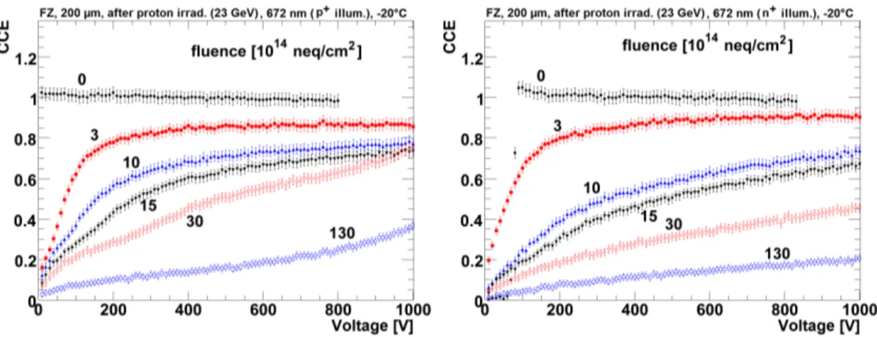
The current signal induced in the pad is read out by a digital oscilloscope with 1 GHz bandwidth and 5 GHz sampling rate (Tektronix DPO 4104). The induced charge, Q, is calculated by integrating the time-resolved current signal over 30 ns, and the charge collection efficiency (CCE) is determined as the ratio of the collected charge after irradiation to that measured for a fully depleted non-irradiated reference sensor at 400 V bias (full-depletion voltage 90 V). The total uncertainty of the CCE determined by this procedure is estimated to be 3%. The main contributions to the uncertainty are a spread of Q after reassembling a sensor into the setup and measuring it again (about 2%) and a systematic uncertainty of Q because of a voltage dependence (about 2%) which is observed for non-irradiated sensors (figure1). The voltage dependence of Q may be explained by the voltage dependent charge collection time in combination with the used electronic circuit and the integration time window of 30 ns. At 30 ns the electronic circuit of the setup leads to negative contributions in the current signal. More details about the setup, the CCE determination, and the CCE uncertainty can be found in ref. [15]. The CCE as a function of bias voltage is shown in figure1. As expected for light with a short penetration depth the CCE is 0 for voltages below full depletion and 1 at voltages above full depletion, if the non-irradiated sensor is illuminated at the n+side.
Five sensors were irradiated at the PS (CERN) with 23 GeV protons. These sensors were not cooled during irradiation, which took up to about two weeks for the highest fluence. They were investigated without additional annealing after irradiation. One sensor was irradiated at KIT (Karlsruhe) with 23 MeV protons. This sensor was cooled during irradiation to below 0◦C and
investigated after 10 minutes of annealing at 60◦C. No significant dependence of the effective
trapping times on annealing time has been observed in ref. [4] for the short term annealing, so that no significant impact is expected as a result of the different annealing scenarios.
3 Simulation of charge collection
The electric field is calculated using Synopsys device simulation,3 assuming two effective traps:
a deep acceptor, A, and a deep donor, D, with energy levels of ED = EV + 0.48 eV and EA =
EC −0.525 eV [10], where EV and EC represent the energy levels of the valence band and the
conduction band. Different defect concentrations and cross sections are used for the different irradiation types and for the different fluences. The values relevant for the studies presented in this paper are reported in table 1. Some values were extracted for silicon sensors after 23 GeV
2016 JINST 11 P04023
proton irradiation from grazing-angle test beam measurements that are described in ref. [11] (inliterature [4, 11] the proton energy is often cited with the full energy of 24 GeV, but in this document we refer to the kinetic energy of 23 GeV). They are used to describe measurements after 23 GeV proton irradiation. The other values are taken from ref. [8]. They were tuned to describe capacitance, current, and time-resolved charge collection measurements on single-pad silicon sensors after 23 MeV proton irradiation. They are used to describe measurements after 23 MeV proton irradiation.
Table 1. The key parameter values used in the Synopsys device simulation. These include: donor and
acceptor concentrations, ND and NA, and their electron and hole capture cross sections, σe,h
D, A, for silicon sensors after irradiation with 23 GeV protons (top rows) [11], and for sensors after irradiation with 23 MeV protons (bottom rows) [8].
φneq NA ND σeA σeD σhA σhD [1014neq/cm2] [1014cm−3] [1014cm−3] [10−15cm2] [10−15cm2] [10−15cm2] [10−15cm2] 2 (23 GeV) [11] 6.8 10 6.6 6.6 1.65 6.6 6 (23 GeV) [11] 16 40 6.6 6.6 1.65 1.65 12 (23 GeV) [11,18]4 30 69 3.8 3.8 0.94 0.94 24 (23 GeV) [11,18]4 61 138 3.8 3.8 0.94 0.94 3 (23 MeV) [8] 4.2 13 10 10 10 10 10 (23 MeV) [8] 12.5 52 10 10 10 10
In figure2it can be seen that the electric field distribution is different for sensors after 23 MeV proton irradiation compared to that simulated for 23 GeV proton irradiation. The figure shows the electric field distribution for the defect values specified in ref. [8], namely, for an irradiation with 23 MeV protons and a fluence of 1015neq/cm2, and for the defect values given in ref. [11] for an
irradiation with 23 GeV protons and a fluence of 1.2 · 1015neq/cm2.
The PixelAV detector simulation package [11] is used to simulate the transport of charge carriers. The effective trapping rates in the simulation are assumed to be constant over the depth of the sensor. Some modifications are made in order to describe the measurements reported here:
• Drift parameters are adjusted to describe the drift in h100i-oriented silicon [19] (changes in the assumed mobility directly impact the resulting trapping rates);
• Charges are generated at the front or the rear side of the sensor with a penetration depth of 3.5 µm to simulate the charge generation by laser light of 672 nm wavelength. The number of charges generated is fixed to 40 000 eh-pairs;
• The induced signal is calculated using a linear weighting potential between front and rear contact;
• The trapping rates are tuned iteratively to match the predicted CCE to the measured CCE.
4 The data for the fluence points 12 · 1014neq/cm2 and 24 · 1014neq/cm2 have not been published. They were determined using the same methods as in ref. [11].
2016 JINST 11 P04023
Figure 1. The CCE as a function of bias voltage is shown for 200 µm thick n-type sensors after differentfluences of 23 GeV proton irradiation. Laser light of 672 nm wavelength is used to generate eh-pairs close to the p+-side (left), so that the signals are dominated by electron drift, or close to the n+-side (right), so that the signal is dominated by hole drift.
Figure 2. The simulated electric field at 600 V as a function of sensor depth, x, for a 200 µm thick n-type
sensor after proton irradiation with different proton energies. The p+implant is at x = 0 µm, and the n+ implant is at x = 200 µm. The field is calculated using parameters from ref. [11] for irradiation with 23 GeV protons (1.2 · 1015neq/cm2) and ref. [8] for irradiation with 23 MeV protons (1 · 1015neq/cm2).
In figure3the resulting time-resolved current signals are shown for three different effective trapping rates and for two different electric fields. For the “no trapping” case, the integrated signals are Q = 40 000 electrons, i.e. all charges are collected (CCE = 1). For the other cases the CCE decreases monotonically with increasing 1/τ. The effective trapping rate can be tuned to reproduce the measured CCE.
4 Comparison of measurements with simulation
In order to compare the simulation to the sensor measurements, the electronic response of the experimental setup must be taken into account. This is achieved by convolving the simulated current signals with the response of the setup to a delta function; the latter is shown in figure4. The response was extracted by studying the charge collection in non-irradiated sensors and has been reported in ref. [17].
2016 JINST 11 P04023
Figure 3. Simulated current signals at 600 V bias for a proton-irradiated 200 µm thick n-type sensor after40 000 eh-pairs are generated instantaneously close to the p+-side. A penetration depth of 3.5 µm is used to simulate light with 672 nm wavelength. The signals are dominated by electron drift. Different electron trapping rates are used: no trapping, trapping tuned to CCE = 0.74 (the value 0.74 is taken from figure1
for φneq = 1015neq/cm2), and trapping according to equation (1.2) with φneq= 1015neq/cm2. For the two proton energies the respective electric field distributions from figure2are used. Left: simulation for 23 GeV protons. Right: simulation for 23 MeV protons.
Figure 4. Transfer characteristic of the circuit (response of the setup to a delta function for the sensor
current).
The simulated current signals, after the electronic response of the setup is taken into account, are compared to measured signals in figure5. The measurements are performed after proton irradiation of 1015neq/cm2 (23 GeV protons) and 1.5 · 1015neq/cm2 (23 GeV protons and 23 MeV protons).
A fluence of 1.5 · 1015neq/cm2is expected after the collection of 3000 fb−1of HL-LHC data at a
radius of 20 cm from the interaction point. In the simulation the effective trapping rates are adjusted so that the simulated CCE agrees with the measured CCE. As seen in figure2the expected electric field distribution is different for sensors after 23 MeV proton irradiation compared to that expected after 23 GeV proton irradiation. The same electric field is used for both fluences (1015neq/cm2and
1.5 · 1015neq/cm2) as there are only limited data available on the two effective traps. For 23 GeV
protons the field is based on parameters tuned to sensors irradiated to 1.2·1015neq/cm2using 23 GeV
protons. For 23 MeV protons the field is based on parameters for the fluence 1015neq/cm2[8] and
2016 JINST 11 P04023
Figure 5. Comparison of simulated and measured current signals, I(t), at 600 V, normalised to the depositedcharge, Q0. The signals are mainly induced by electrons drifting from the front side to the rear side of the sensor. The results from a 200 µm thick n-type sensor are shown after 23 GeV proton irradiation to a fluence of 1015neq/cm2(left) and 1.5 · 1015neq/cm2(right), and after 23 MeV proton irradiation to a fluence of 1.5 · 1015neq/cm2 (right). At 1015neq/cm2 no sensors that were irradiated with 23 MeV protons are available.
The simulated current signals are in good agreement with the measured currents, especially in light of the crude assumptions used in the simulation. Taking into account the fact that the measured pulse shapes are quite different after 23 GeV proton irradiation compared to after 23 MeV proton irradiation (figure 5), it is clear that different electric field distributions must be used for sensors that have undergone 23 MeV proton irradiation versus those that have undergone 23 GeV proton irradiation. However, even if quite different electric field distributions are used, the measured CCE is reproduced using similar trapping rates for the two cases (figure3).
5 Extracted trapping rates
The effective trapping rates that provide the best description of the measurements in terms of CCE are listed in table2. They are also shown in figure6, where they are compared to the trapping rates reported in refs. [4,8,11]. For 3 · 1014neq/cm2 the results show little dependence on the electric
field: they are the same regardless of whether the parameters for 2·1014neq/cm2or 6·1014neq/cm2
(table1) are used. For 3·1015neq/cm2the electric field was calculated according to ref. [11] with the
electric field tuned to describe pixel sensors irradiated with a similar fluence of 2.4 · 1015neq/cm2.
The CCE uncertainties quoted in table2 are the statistical and systematic uncertainties added in quadrature. To determine the E-field uncertainty different electric field distributions were tested, for each fluence the two that correspond to the closest fluences available, e.g. for 1 · 1015neq/cm2
the values in table1are used to calculate the electric fields that correspond to 6 · 1014neq/cm2and
to 1.2 · 1015neq/cm2. The CCE measurements taken at the highest fluence of 1.3 · 1016neq/cm2
(figure1) are not analysed, since no simulation of the electric field at similar fluences is available. For electron trapping the results of this work are compatible with the results presented in refs. [4,8,11] for the fluences studied there. However, it is clear that the results presented in ref. [4] cannot be extrapolated to fluences of 1015neq/cm2 and above as this leads to an overestimate of
2016 JINST 11 P04023
Table 2. Trapping rates extracted from the CCE at T = −20◦C and V = 600 V after irradiation with 23 GeVprotons. Note that the trapping rates are effective rates describing the CCE for electrons drifting from the p-n junction to the rear side, and holes drifting from the rear side to the p-n junction.
φneq [neq/cm2] 1/τ
e[1/ns] 1/τh[1/ns]
3 · 1014 0.145 ±0.035(CCE) ±0.005(E-field) 0.085 ±0.025(CCE) ±0.005(E-field)
1 · 1015 0.30 ±0.04(CCE) ±0.03(E-field) 0.38 ±0.04(CCE) ±0.04(E-field)
1.5 · 1015 0.42 ±0.04(CCE) ±0.03(E-field) 0.49 ±0.05(CCE) ±0.03(E-field)
3 · 1015 0.55 ±0.06(CCE) ±0.06(E-field) 0.98 ±0.10(CCE) ±0.12(E-field)
Figure 6. Effective trapping rates for electrons (left) and holes (right) at V = 600 V according to this study
(23 GeV protons, T = −20◦C) compared to studies by G. Kramberger et al. [4] (23 GeV protons, T = −10◦C), M. Swartz et al. [11] (23 GeV protons, T = −10◦C), and R. Eber [8] (23 MeV protons, T = −10◦C). The vertical error bars show the CCE uncertainties (table2). No significant difference has been observed between T = −10◦C and T = −20◦C.
in refs. [6, 8]. For hole trapping lower trapping rates compared to refs. [4] and [11] are already observed at 3 · 1014neq/cm2. This corresponds to the high CCE measured at this fluence (figure1).
Note that for our measurements higher bias voltages and thinner sensors are used compared to those analysed in ref. [4] and that in ref. [11] the trapping rates are based on those from ref. [4].
For one irradiation (1·1015neq/cm2of 23 GeV protons) the electron trapping rate was extracted
not only at 600 V but also at 400 V and at 900 V. For this fluence we do not expect charge multi-plication below 1000 V, since charge multimulti-plication starts to be relevant only above 120 kV/cm [7]. Simulated fields are below 70 kV/cm at 600 V (figure2). Only for higher fluences of 3·1015neq/cm2
and above the CCE measurements indicate charge multiplication for electrons above 800 V (fig-ure1). It is found that the trapping rates are similar, but slightly higher at 400 V (0.33 ns−1) and
slightly smaller at 900 V (0.28 ns−1) compared to the rate at 600 V (0.3 ns−1). Similar effects have
been reported in refs. [6,7]. However, due to the uncertainties in the order of 10% (table2), which are partly systematic uncertainties, it is not clear whether this effect is significant.
2016 JINST 11 P04023
Figure 7. CCE as a function of bias voltage for 200 µm thick n-type sensors after irradiation with differentfluences of 23 GeV protons. Laser light of 1062 nm wavelength was used to generate eh-pairs throughout the whole sensor depth.
6 Applicability to eh-pairs generated along the sensor depth
To test the applicability of the results reported in table2to cases where eh-pairs are generated along the whole sensor depth (as is the case for charged particles traversing the sensor) further simulations are performed and compared to the measurements.
A separate simulation is performed in which eh-pairs are generated along the whole sensor depth using an attenuation length of 1 000 µm. The simulation was used to describe CCE measurements where eh-pairs are generated using light of 1062 nm wavelength (front-side illumination). The measured CCE as a function of bias voltage is shown in figure7and a comparison of the simulated and measured CCE at 600 V bias is presented in table3.
The simulated CCE is, on average, 0.06 below the measured CCE if the trapping rates from table2(simulation A) are used. This indicates that the effective trapping rates for the measurements using 1062 nm light are lower than for the measurements where eh-pairs are generated close to the implants only. This is expected if the leakage current leads to a non-uniform occupation of defects that are relevant for trapping. We conclude that charge losses might be overestimated if the rates given in table2are used to predict charge collection in cases where eh-pairs are generated along the whole sensor depth. However, compared to the widely used extrapolation of effective trapping rates at low fluences the overestimation is significantly reduced (table3).
The results presented here may be used in further simulations of irradiated silicon sensors. Due to the complex (and sometimes non-linear) generation of defects in the irradiation process we have not described the results with a parameterisation. Instead a linear interpolation may be used to simulate fluences lying in between those considered in this work. For significantly different bias voltages a correction may be applied (effective trapping rates appear about 10% higher when the bias voltage is decreased by 200 V). The applicability of the results was not tested using segmented sensors. However, comparison with other studies [11] shows that similar values of the effective trapping rates are used to describe data in strip sensors (figure6).
2016 JINST 11 P04023
Table 3. Simulated values of the CCE compared to measurements at 600 V using 1062 nm light to generateeh-pairs. In simulation A, the trapping parameters from table 2 are used, in simulation B, extrapolated trapping rates (equation (1.2), βe= 5.8 · 10−16cm2/ns, βh = 8.2 · 10−16cm2/ns) according to ref. [4] are used.
φneq[neq/cm2] CCE measured CCE simulated A CCE simulated B
3 · 1014 0.93 ± 0.03 0.92 ± 0.03 0.85 ± 0.02
1 · 1015 0.85 ± 0.03 0.76 ± 0.03 0.60 ± 0.03
1.5 · 1015 0.75 ± 0.03 0.70 ± 0.03 0.50 ± 0.03
3 · 1015 0.60 ± 0.03 0.51 ± 0.03 0.27 ± 0.02
7 Summary
Time-resolved charge collection measurements using red laser light of 672 µm wavelength have been used to determine the effective trapping rates for electrons (holes) moving from the p+ to
the n+(n+to the p+) contact in silicon single-pad sensors irradiated with protons with fluences up
to 3 · 1015neq/cm2. Light of this wavelength has a penetration depth of about 3.5 µm in silicon.
The time-resolved measurements are described using simulation. The electric fields have been calculated assuming two effective traps with energy levels, concentrations, and cross-sections taken from the literature [8,10,11].
It is found that at the lowest investigated fluence (3·1014neq/cm2) the effective electron trapping
rate is compatible with the results presented in ref. [4] using fluences up to 2.4 · 1014neq/cm2.
However, at higher fluences the extracted trapping rates are a factor of 2–3 below the trapping rates expected if the results from ref. [4] are extrapolated. The effective hole trapping rates are also a factor of up to about 3 below the extrapolations. These results confirm previous studies that found higher signals than expected at high fluences [6–8] and are important for the description of the tracker performances after a few years of operation at the High-Luminosity LHC.
Acknowledgments
The research leading to these results has received funding from the European Commission under the FP7 Research Infrastructures project AIDA, grant agreement no. 262025. The information herein only reflects the views of its authors and not those of the European Commission and no warranty expressed or implied is made with regard to such information or its use. Support was also provided by the Helmholtz Alliance “Physics at the Terascale” and the German Ministry of Science, BMBF, through the Forschungsschwerpunkt “Particle Physics with the CMS-Experiment”. The measurements presented in this document have been performed at the University of Hamburg.
References
[1] ATLAS collaboration, Letter of Intent for the Phase-II Upgrade of the ATLAS Experiment,
CERN-LHCC-2012-022(2012).
[2] CMS collaboration, Technical Proposal for the Phase-II Upgrade of the Compact Muon Solenoid,
2016 JINST 11 P04023
[3] M. Moll, Radiation Damage in Silicon Particle Detectors, Ph.D. Thesis, University of Hamburg,Hamburg Germany (1999).
[4] G. Kramberger et al., Effective trapping time of electrons and holes in different silicon materials irradiated with neutrons, protons and pions,Nucl. Instrum. Meth. A 481(2002) 297.
[5] G. Kramberger et al., Determination of effective trapping times for electrons and holes in irradiated silicon,Nucl. Instrum. Meth. A 476(2002) 645.
[6] J. Lange, Radiation Damage in Proton-Irradiated Epitaxial Silicon Detectors, MSc Thesis, University of Hamburg, Hamburg Germany, DESY-THESIS-2009-022 (2008).
[7] T. Pöhlsen, Charge Collection and Space Charge Distribution in Neutron-Irradiated Epitaxial Silicon Detectors, MSc Thesis, University of Hamburg, Hamburg Germany, DESY-THESIS-2010-013 (2010).
[8] R. Eber, Untersuchung neuartiger Sensorkonzepte und Entwicklung eines effektiven Modells der Strahlenschädigung für die Simulation hochbestrahlter Silizium-Teilchendetektoren, Ph.D. Thesis, Karlsruhe Institut für Technologie (KIT), Karlsruhe Germany, IEKP-KA/2013-27 (2013).
[9] E. Borchi, M. Bruzzi, Z. Li and S. Pirollo, A two-level model for heavily irradiated silicon detectors, Nucl. Instrum. Meth. A 425(1999) 343.
[10] V. Eremin, Z. Li and E. Verbitskaya, The origin of double peak electric field distribution in heavily irradiated silicon detectors,Nucl. Instrum. Meth. A 476(2002) 556.
[11] M. Swartz et al., Simulation of Heavily Irradiated Silicon Pixel Detectors,physics/0605215.
[12] A. Dierlamm on behalf of the CMS Tracker collaboration, CMS HPK sensor characterisation,
PoS(Vertex 2012)016.
[13] G. Steinbrück for the CMS Tracker collaboration, Towards Radiation Hard Sensor Materials for the CMS Tracker Upgrade,CMS-CR-2012-308(2012).
[14] T. Poehlsen on behalf of the CMS Tracker collaboration, Radiation hard silicon sensors for the CMS tracker upgrade,CMS-CR-2013-405(2013).
[15] T. Poehlsen, Charge Losses in Silicon Sensors and Electric-Field Studies at the Si-SiO2Interface, Ph.D. Thesis, University of Hamburg, Hamburg Germany, DESY-THESIS-2013-025 (2013). [16] J. Erfle, Irradiation study of different silicon materials for the CMS tracker upgrade, Ph.D. Thesis,
University of Hamburg, Hamburg Germany, DESY-THESIS-2014-010 (2014).
[17] C. Scharf and R. Klanner, Determination of the electronics transfer function for current transient measurements,arXiv:1407.2761.
[18] M. Swartz, private communication.
[19] J. Becker, E. Fretwurst and R. Klanner, Measurements of charge carrier mobilities and drift velocity saturation in bulk silicon of h111i and h100i crystal orientation at high electric fields,Solid State Electron. 56(2011) 104.
2016 JINST 11 P04023
Tracker group of the CMS collaboration
Institut für Hochenergiephysik der Österreichischen Akademie der Wissenschaften (HEPHY), Vienna, Austria
W. Adam, T. Bergauer, M. Dragicevic, M. Friedl, R. Fruehwirth, M. Hoch, J. Hrubec, M. Krammer, W. Treberspurg, W. Waltenberger
Universiteit Antwerpen, Belgium
S. Alderweireldt, W. Beaumont, X. Janssen, S. Luyckx, P. Van Mechelen, N. Van Remortel, A. Van Spilbeeck
Brussels-ULB, Belgium
P. Barria, C. Caillol, B. Clerbaux, G. De Lentdecker, D. Dobur, L. Favart, A. Grebenyuk, Th. Lenzi, A. Léonard, Th. Maerschalk, A. Mohammadi, L. Perniè, A. Randle-Conde, T. Reis, T. Seva, L. Thomas, C. Vander Velde, P. Vanlaer, J. Wang, F. Zenoni
Brussels-VUB, Belgium
S. Abu Zeid, F. Blekman, I. De Bruyn, J. D’Hondt, N. Daci, K. Deroover, N. Heracleous, J. Keaveney, S. Lowette, L. Moreels, A. Olbrechts, Q. Python, S. Tavernier, P. Van Mulders, G. Van Onsem, I. Van Parijs, D.A. Strom
CP3/IRMP - Université catholique de Louvain - Louvain-la-Neuve – Belgium
S. Basegmez, G. Bruno, R. Castello, A. Caudron, L. Ceard, B. De Callatay, C. Delaere,
T. Du Pree, L. Forthomme, A. Giammanco, J. Hollar, P. Jez, D. Michotte, C. Nuttens, L. Perrini, D. Pagano, L. Quertenmont, M. Selvaggi, M. Vidal Marono
University of Mons, Belgium
N. Beliy, T. Caebergs, E. Daubie, G.H. Hammad
Helsinki Institute of Physics, Finland
J. Härkönen, T. Lampén, P.-R. Luukka, T. Mäenpää, T. Peltola, E. Tuominen, E. Tuovinen
University of Helsinki and Helsinki Institute of Physics, Finland
P. Eerola
Lappeenranta University of Technology, Lappeenranta, Finland
T. Tuuva
Université de Lyon, Université Claude Bernard Lyon 1, CNRS/IN2P3, Institut de Physique Nucléaire de Lyon, France
G. Beaulieu, G. Boudoul, C. Combaret, D. Contardo, G. Gallbit, N. Lumb, H. Mathez, L. Mirabito, S. Perries, D. Sabes, M. Vander Donckt, P. Verdier, S. Viret, Y. Zoccarato
Groupe de Recherches en Physique des Hautes Energies, Université de Haute Alsace, Mulhouse, France
2016 JINST 11 P04023
Institut Pluridisciplinaire Hubert Curien, Université de Strasbourg, IN2P3-CNRS, Strasbourg, France
J. Andrea, D. Bloch, C. Bonnin, J.-M. Brom, E. Chabert, L. Charles, Ch. Goetzmann, L. Gross, J. Hosselet, C. Mathieu, M. Richer, K. Skovpen
I. Physikalisches Institut, RWTH Aachen University, Germany
C. Pistone, G. Fluegge, A. Kuensken, M. Geisler, O. Pooth, A. Stahl
III. Physikalisches Institut, RWTH Aachen University, Germany
C. Autermann, M. Edelhoff, H. Esser, L. Feld, W. Karpinski, K. Klein, M. Lipinski, A. Ostapchuk, G. Pierschel, M. Preuten, F. Raupach, J. Sammet, S. Schael, G. Schwering, B. Wittmer,
M. Wlochal, V. Zhukov
DESY, Hamburg, Germany
N. Bartosik, J. Behr, A. Burgmeier, L. Calligaris, G. Dolinska, G. Eckerlin, D. Eckstein, T. Eichhorn, G. Fluke, J. Garay Garcia, A. Gizhko, K. Hansen, A. Harb, J. Hauk,
A. Kalogeropoulos, C. Kleinwort, I. Korol, W. Lange, W. Lohmann, R. Mankel, H. Maser, G. Mittag, C. Muhl, A. Mussgiller, A. Nayak, E. Ntomari, H. Perrey, D. Pitzl, M. Schroeder, C. Seitz, S. Spannagel, A. Zuber
University of Hamburg, Germany
H. Biskop, V. Blobel, P. Buhmann, M. Centis-Vignali, A.-R. Draeger, J. Erfle, E. Garutti, J. Haller, M. Hoffmann, A. Junkes, T. Lapsien, S. Mättig, M. Matysek, A. Perieanu, J. Poehlsen,
T. Poehlsen, Ch. Scharf, P. Schleper, A. Schmidt, V. Sola, G. Steinbrück, J. Wellhausen
Karlsruhe-IEKP, Germany
T. Barvich, Ch. Barth, F. Boegelspacher, W. De Boer, E. Butz, M. Casele, F. Colombo, A. Dierlamm, R. Eber, B. Freund, F. Hartmann1, Th. Hauth, S. Heindl, K.-H. Hoffmann,
U. Husemann, A. Kornmeyer, S. Mallows, Th. Muller, A. Nuernberg, M. Printz, H. J. Simonis, P. Steck, M. Weber, Th. Weiler
Department of Physics and Astrophysics, University of Delhi, Delhu, India
A. Bhardwaj, A. Kumar, A. Kumar, K. Ranjan
Institute for Research in Fundamental Sciences (IPM), Tehran, Iran
H. Bakhshiansohl, H. Behnamian, M. Khakzad, M. Naseri
INFN Bari, Italy
P. Cariola, G. De Robertis, L. Fiore, M. Franco, F. Loddo, G. Sala, L. Silvestris
INFN and Dipartimento Interateneo di Fisica, Bari, Italy
D. Creanza, M. De Palma, G. Maggi, S. My, G. Selvaggi
INFN and University of CATANIA, Italy
S. Albergo, G. Cappello, M. Chiorboli, S. Costa, F. Giordano, A. Di Mattia, R. Potenza, M.A. Saizu2, A. Tricomi, C. Tuvè
INFN Firenze, Italy
2016 JINST 11 P04023
INFN and University of Firenze, Italy
V. Ciulli, R. D’Alessandro, S. Gonzi, V. Gori, E. Focardi, P. Lenzi, E. Scarlini, A. Tropiano, L. Viliani
INFN Genova, Italy
F. Ferro, E. Robutti
INFN and University of Genova, Italy
M. Lo Vetere
INFN Milano-Bicocca, Italy
S. Gennai, S. Malvezzi, D. Menasce, L. Moroni, D. Pedrini
INFN and Universita degli Studi di Milano-Bicocca, Italy
M. Dinardo, S. Fiorendi, R.A. Manzoni
INFN Padova, Italy
P. Azzi, N. Bacchetta
INFN and University of Padova, Italy
D. Bisello, M. Dall’Osso, T. Dorigo, P. Giubilato, N. Pozzobon, M. Tosi, A. Zucchetta
INFN Pavia and University of Bergamo, Italy
F. De Canio, L. Gaioni, M. Manghisoni, B. Nodari, V. Re, G. Traversi
INFN Pavia and University of Pavia, Italy
D. Comotti, L. Ratti
INFN Perugia, Italy
G. M. Bilei, L. Bissi, B. Checcucci, D. Magalotti3, M. Menichelli, A. Saha, L. Servoli, L. Storchi
INFN and University of Perugia, Italy
M. Biasini, E. Conti, D. Ciangottini, L. Fanò, P. Lariccia, G. Mantovani, D. Passeri, P. Placidi, M. Salvatore, A. Santocchia, L.A. Solestizi, A. Spiezia
INFN Pisa, Italy
K. Androsov4, P. Azzurri, S. Arezzini, G. Bagliesi, A. Basti, T. Boccali, F. Bosi, R. Castaldi,
A. Ciampa, M. A. Ciocci4, R. Dell’Orso, G. Fedi, A. Giassi, M. T. Grippo4, T. Lomtadze,
G. Magazzu, E. Mazzoni, M. Minuti, A. Moggi, C. S. Moon4, F. Morsani, F. Palla, F. Palmonari,
F. Raffaelli, A. Savoy-Navarro5, A.T. Serban6, P. Spagnolo, R. Tenchini, A. Venturi, P.G. Verdini
University of Pisa and INFN Pisa, Italy
L. Martini, A. Messineo, A. Rizzi, G. Tonelli
Scuola Normale Superiore di Pisa and INFN Pisa, Italy
F. Calzolari, S. Donato, F. Fiori, F. Ligabue, C. Vernieri
INFN Torino, Italy
2016 JINST 11 P04023
INFN and University of Torino, Italy
R. Bellan, S. Casasso, M. Costa, R. Covarelli, E. Migliore, E. Monteil, M. Musich, L. Pacher, F. Ravera, A. Romero, A. Solano, P. Trapani
Instituto de Fısica de Cantabria (IFCA), CSIC-Universidad de Cantabria, Santander, Spain
R. Jaramillo Echeverria, M. Fernandez, G. Gomez, D. Moya, F.J. Gonzalez Sanchez, F.J. Munoz Sanchez, I. Vila, A.L. Virto
European Organization for Nuclear Research (CERN), Geneva, Switzerland
D. Abbaneo, I. Ahmed, E. Albert, G. Auzinger, G. Berruti, G. Bianchi, G. Blanchot, H. Breuker, D. Ceresa, J. Christiansen, K. Cichy, J. Daguin, M. D’Alfonso, A. D’Auria, S. Detraz,
S. De Visscher, D. Deyrail, F. Faccio, D. Felici, N. Frank, K. Gill, D. Giordano, P. Harris, A. Honma, J. Kaplon, A. Kornmayer, L. Kottelat, M. Kovacs, M. Mannelli, A. Marchioro, S. Marconi, S. Martina, S. Mersi, S. Michelis, M. Moll, A. Onnela, T. Pakulski, S. Pavis, A. Peisert, J.-F. Pernot, P. Petagna, G. Petrucciani, H. Postema, P. Rose, M. Rzonca, M. Stoye, P. Tropea, J. Troska, A. Tsirou, F. Vasey, P. Vichoudis, B. Verlaat, L. Zwalinski
ETH Zürich, Zürich, Switzerland
F. Bachmair, R. Becker, L. Bäni, D. di Calafiori, B. Casal, L. Djambazov, M. Donega, M. Dünser, P. Eller, C. Grab, D. Hits, U. Horisberger, J. Hoss, G. Kasieczka, W. Lustermann, B. Mangano, M. Marionneau, P. Martinez Ruiz del Arbol, M. Masciovecchio, L. Perrozzi, U. Roeser, M. Rossini, A. Starodumov, M. Takahashi, R. Wallny
University of Zürich, Switzerland
C. Amsler7, K.Bösiger, L. Caminada, F. Canelli, V. Chiochia, A. de Cosa, C. Galloni, T. Hreus,
B. Kilminster, C. Lange, R. Maier, J. Ngadiuba, D. Pinna, P. Robmann, S. Taroni, Y. Yang
Paul Scherrer Institut, Villigen, Switzerland
W.Bertl, K. Deiters, W. Erdmann, R. Horisberger, H.-C. Kaestli, D. Kotlinski, U. Langenegger, B. Meier, T. Rohe, S. Streuli
National Taiwan University, Taiwan, ROC
P.-H. Chen, C. Dietz, U. Grundler, W.-S. Hou, R.-S. Lu, M. Moya, R. Wilken
University of Bristol, Bristol, United Kingdom
D. Cussans, H. Flacher, J. Goldstein, M. Grimes, J. Jacob, S. Seif El Nasr-Storey
Brunel University, Uxbridge, United Kingdom
J. Cole, P. Hobson, D. Leggat, I. D. Reid, L. Teodorescu
Imperial College, London, United Kingdom
R. Bainbridge, P. Dauncey, J. Fulcher, G. Hall, A.-M. Magnan, M. Pesaresi, D. M. Raymond, K. Uchida
STFC, Rutherford Appleton Laboratory, Chilton, Didcot, United Kingdom
2016 JINST 11 P04023
Brown University, Providence, Rhode Island, USA
A. Garabedian, U. Heintz, M. Narain, J. Nelson, S. Sagir, T. Speer, J. Swanson, D. Tersegno, J. Watson-Daniels
University of California, Davis, California, USA
M. Chertok, J. Conway, R. Conway, C. Flores, R. Lander, D. Pellett, F. Ricci-Tam, M. Squires, J. Thomson, R. Yohay
University of California, Riverside, California, USA
K. Burt, J. Ellison, G. Hanson, M. Malberti, M. Olmedo
University of California, San Diego, California, USA
G. Cerati, V. Sharma, A. Vartak, A. Yagil, G. Zevi Della Porta
University of California, Santa Barbara, California, USA
V. Dutta, L. Gouskos, J. Incandela, S. Kyre, N. McColl, S. Mullin, D. White
University of Colorado, Boulder, Colorado, USA
J.P. Cumalat, W.T. Ford, A. Gaz, M. Krohn, K. Stenson, S.R. Wagner
Fermi National Accelerator Laboratory (FNAL), Batavia, Illinois, USA
B. Baldin, G. Bolla, K. Burkett, J. Butler, H. Cheung, J. Chramowicz, D. Christian, W.E. Cooper, G. Deptuch, G. Derylo, C. Gingu, S. Gruenendahl, S. Hasegawa, J. Hoff, J. Howell, M. Hrycyk, S. Jindariani, M. Johnson, A. Jung, U. Joshi, F. Kahlid, C. M. Lei, R. Lipton, T. Liu, S. Los, M. Matulik, P. Merkel, S. Nahn, A. Prosser, R. Rivera, A. Shenai, L. Spiegel, N. Tran, L. Uplegger, E. Voirin, H. Yin
University of Illinois, Chicago, Illinois, USA
M.R. Adams, D.R. Berry, A. Evdokimov, O. Evdokimov, C.E. Gerber, D.J. Hofman, B.K. Kapustka, C. O’Brien, D.I. Sandoval Gonzalez, H. Trauger, P. Turner
Purdue University Calumet, Hammond, Indiana, USA
N. Parashar, J. Stupak, III
Purdue University, West Lafayette, Indiana, USA
D. Bortoletto, M. Bubna, N. Hinton, M. Jones, D.H. Miller, X. Shi
University of Iowa, Iowa City, Iowa, USA
P. Tan
University of Kansas, Lawrence, Kansas, USA
P. Baringer, A. Bean, G. Benelli, J. Gray, D. Majumder, D. Noonan, S. Sanders, R. Stringer
Kansas State University, Manhattan, Kansas, USA
A. Ivanov, M. Makouski, N. Skhirtladze, R. Taylor
Johns Hopkins University, Baltimore, Maryland, USA
I. Anderson, D. Fehling, A. Gritsan, P. Maksimovic, C. Martin, K. Nash, M. Osherson, M. Swartz, M. Xiao
2016 JINST 11 P04023
University of Mississippi, Mississippi, USA
J.G. Acosta, L.M. Cremaldi, S. Oliveros, L. Perera, D. Summers
University of Nebraska, Lincoln, Nebraska, USA
K. Bloom, S. Bose, D.R. Claes, A. Dominguez, C. Fangmeier, R. Gonzalez Suarez, F. Meier, J. Monroy
Northwestern University, Evanston, Illinois, USA
K. Hahn, S. Sevova, K. Sung, M. Trovato
Rutgers University, Piscataway, New Jersey, USA
E. Bartz, D. Duggan, E. Halkiadakis, A. Lath, M. Park, S. Schnetzer, R. Stone, M. Walker
University of Puerto Rico, Mayaguez, Puerto Rico, USA
S. Malik, H. Mendez, J.E. Ramirez Vargas
State University of New York, Buffalo, New York, USA
M. Alyari, J. Dolen, J. George, A. Godshalk, I. Iashvili, J. Kaisen, A. Kharchilava, A. Kumar, S. Rappoccio
Cornell University, Ithaca, New York, USA
J. Alexander, J. Chaves, J. Chu, S. Dittmer, G. Kaufman, N. Mirman, A. Ryd, E. Salvati, L. Skinnari, J. Thom, J. Thompson, J. Tucker, L. Winstrom
Rice University, Houston, Texas, USA
B. Akgün, K.M. Ecklund, T. Nussbaum, J. Zabel
University of Rochester, New York, USA
B. Betchart, R. Covarelli, R. Demina, O. Hindrichs, G. Petrillo
Texas A&M University, College Station, Texas, USA
R. Eusebi, I. Osipenkov, A. Perloff, K.A. Ulmer
Vanderbilt University, Nashville, Tennessee, USA
A. G. Delannoy, P. D’Angelo, W. Johns
1: Also at CERN, European Organization for Nuclear Research, Geneva, Switzerland
2: Also at Horia Hulubei National Institute of Physics and Nuclear Engineering (IFIN-HH), Bucharest, Romania
3: Also at Modena and Reggio Emilia University, Italy 4: Also at University of Siena, Italy
5: Also at CNRS-IN2P3, Paris, France
6: Also at University of Bucharest, Bucharest, Romania 7: Now at University of Bern, Switzerland