Array of plasmonic Vivaldi antennas coupled to
silicon waveguides for wireless networks
through on-chip optical technology - WiNOT
G
IOVANNAC
ALÒ,
1G
AETANOB
ELLANCA,
2B
ADRULA
LAM,
1A
LIE
MREK
APLAN,
2P
AOLOB
ASSI,
3 ANDV
INCENZOP
ETRUZZELLI,
1,* 1Department of Electrical and Information Engineering, Polytechnic of Bari, Via Orabona, 4, Bari 70125, Italy2Department of Engineering, University of Ferrara, Via Saragat, 1, Ferrara 44122, Italy
3Department of Electrical, Electronic and Information Engineering, University of Bologna, Viale del Risorgimento, 2, Bologna 40136, Italy
Abstract: Optical technology applied to on-chip wireless communication is particularly promising to overcome the performance limitations of the state-of-the-art networks on-chip. A key enabling component for such applications is the plasmonic antenna coupled to conventional silicon waveguides, which can guarantee full compatibility with standard optical circuitry. In this paper, we propose an antenna array configuration based on tilted plasmonic Vivaldi antennas coupled to a silicon waveguide. The details of the single antenna and of the array design are reported. The radiation characteristics of the array are suitable for on-chip point-to-point communication, i.e. in-plane maximum gain of 14.70 dB for an array with five antennas. The array exploits a travelling wave feeding scheme and, therefore, is compact in size (about 3.5 µm x 8.7 µm).
© 2018 Optical Society of America under the terms of theOSA Open Access Publishing Agreement
1. Introduction
Wireless networks implemented through on chip optical technology (WiNOT) can allow to overcome the limitations of conventional electronic and optical networks on-chip. The possibility of controlling the on-chip radiation of optical signals through antennas is the basis for a completely new approach to communication. Thanks to the wireless optical transmission, this approach can improve the performances in terms of speed, bandwidth and energy consumption, relieving, at the same time, the network topological constraints [1–3]. A promising field of application of such a technology is the inter- and intra-core communication in Chip Multiprocessors (CMP), where the on-chip wireless communication at optical frequencies can combine, at the chip level, the well known advantages of wireless communications with those pertaining to photonics.
Architectures based on "wired" Optical Network-on-Chip (ONoC), which exploit an optical layer housing a large number of waveguide components, have been successfully proposed for improving the communication among different cores in the optical domain [4-7]. However, the advantages of wired optical networks often find a counterpart in the complex layout, the sophisticated routing algorithms, and the high power budget. Moreover, as the network size scales up, signal losses and crosstalk due to waveguide crossings dramatically increase [8–10]. The on-chip wireless connection through optical nanoantennas can mitigate these limitations and increase the versatility in the network topology design.
Evidences of the advantages of wireless optical communication have been already demonstrated for free-space in-door optical wireless networks. In fact, free-space optical communication is particularly interesting for long-range line-of-sight connections thanks to the high bandwidth and to the immunity to electromagnetic interference. In this context, the implementation of
#341346
integrated optical phased arrays (OPA) has provided simple and precise free-space optical beam steering through the engineering of significant parameters such as emitter spacing, phase shift between adjacent elements, and emitter aperture, which lead to higher directivity and path reconfigurability [11–13].
The on-chip integration of miniaturized optical radiating elements, such as nanoantennas, can enable optical wireless communication also at the chip-scale. Furthermore, by properly designing the radiating elements and by engineering the antenna radiation patterns, the on-chip wireless systems can be empowered by signal path reconfigurability and beam forming, which can enable novel signal routing schemes and scalable photonic architectures. It is also worth mentioning that the potentiality of the integrated on-chip wireless technology is not limited to signal communication, but it can allow completely different applications such as the generation of complex beams for material processing, the optical tweezing, and the biological sensing for lab-on-a-chip systems, as proposed in [1].
The key component in WiNOT is indeed the antenna radiating at the optical frequencies. Recent researches have successfully proposed different all-dielectric [1] and all-plasmonic antennas [14–16] for wireless communications. All-dielectric antennas, made of tapered waveguides with dielectric directors, are very promising since they exhibit high directivities and low losses, but are large in size (e.g. about 15-µm long antennas are proposed in [1]). Plasmonic antennas are much more compact, but the solutions proposed in the literature for wireless applications are generally based on all-plasmonic structures, which do not address the problem of integrating such devices within SOI-based optical networks. An alternative solution to all-dielectric and all-plasmonic radiators are the waveguide-coupled plasmonic antennas [17–21]. The advantages of such antennas are more compact sizes and, at the same time, the full compatibility with conventional integrated optical components. In this way, waveguide-coupled plasmonic antennas enable also an hybrid wired/wireless approach in the network design. The efficient coupling between plasmonic antennas and SOI waveguides is non-trivial, especially because an on-chip point-to-point connection requires in-plane radiation (i.e. maximum of the directivity in the plane of the network). An efficient coupling between SOI waveguides and plasmonic particle chains (i.e. chains of metal ellipses) was demonstrated in [17,18]. If suitably designed, these metallic structures can behave as directive radiators, but the previleged radiation direction is off-chip. Solutions, using plasmonic antennas with hybrid-waveguide feeding [19–21], have been also proposed for wireless applications. However, hybrid plasmonic-dielectric waveguides are not fully compatible with the standard SOI ones. In [22] the authors proposed a single Vivaldi antenna coupled to a truncated silicon waveguide. The optical power in input to the waveguide is transferred to the antenna, through a vertical directional coupler, and then radiated in the surrounding medium in the direction of the propagation in the Siwaveguide. Moreover, starting from the antenna configuration in [22], in [23] the authors proposed a two-element antenna array fed by a waveguide signal splitter. The structure achieved a 3 dB improvement of the gain with respect to the single antenna (i.e. G = 9.9 dB). In the case of the array proposed in [23], in order to increase the number of antennas, an N-ways signal splitter must be designed, which constraints the overall size of the array.
In this paper, we propose an array of plasmonic Vivaldi antennas, coupled to a single silicon waveguide, designed for C-band operation. The array exploits a traveling wave excitation implemented by coupling 90°-tilted antennas to the same Si waveguide. The geometrical rotation of the antenna allows a 90°-tilt of the radiation pattern with respect to the waveguide propagation direction. Moreover, it allows the implementation of a compact antenna array fed by a single waveguide, capable of improving the radiation performances in terms of directivity and gain, with respect to the single antenna case. In the following we will first describe the design and the analysis of a single tilted Vivaldi antenna coupled to the Si waveguide and then we will report the results of the array design.
2. Tilted Vivaldi antenna array
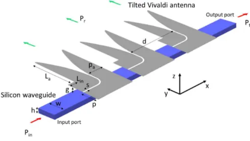
The proposed structure, schematized in Fig. 1, is made of a silicon waveguide coupled to an array of silver Vivaldi antennas. The silver metal was chosen for its relatively low losses (with imaginary part of the refractive index k = 11.57 at the wavelength λ = 1.55 µm), however the design procedure proposed in this paper has a general validity and it can be virtually applied to metals typically used in CMOS platforms (e.g. aluminium, copper, etc,). The overall structure is embedded in an homogeneous medium, equivalent to SiO2, with refractive index nSiO2=1.444. The optical signal (Pin) is launched in input to the Si waveguide and it is vertically coupled to the antennas, which are separated from the waveguide by a dielectric layer of thickness g. Each antenna is obtained by shaping a plasmonic slot waveguide according to a Vivaldi profile and it is 90°-tilted with respect to the propagation direction (x) of the optical signal in the Si waveguide. In this way, the signal coupled to the antenna array is radiated (Pr) in the positive y direction (i.e. the direction of the antenna aperture denoted by the green arrows).
Fig. 1. Scheme of the tilted Vivaldi antenna array coupled to the Si waveguide.
2.1. Design of the cross-section parameters
The design of the single antenna aims at efficiently transferring the optical signal, propagating in the Si waveguide, to the antenna and at radiating it in the surrounding medium. However, we must consider that the proposed array is excited by a traveling wave, since all the antennas share the same feeding waveguide. Therefore, not all the signal power must be transferred to each of the antennas in the array and partial, but efficient, coupling with the Si waveguide is required. Moreover, since the structure is meant for on-chip wireless applications, in-plane radiation is desired to allow point-to-point communication (i.e. maximum radiation in the xy plane).
The coupling between the Si and the slot waveguide, constituting the antenna, happens both in the region where the slot runs parallel to the Si waveguide (straight region denoted by Lin in Fig. 1) and in the region where the slot bends. The straight input region behaves as a directional coupler with constant coupling coefficient. Therefore, the coupling of the signal to the antenna depends on the geometrical sizes of both the Si waveguide (i.e. width w and height h) and the plasmonic slot waveguide constituting the antenna (i.e. width p, slot width s, and Ag layer thickness t).
SOI substrates for photonic applications. Moreover, fabrication compatible values of the Ag layer thickness t = 50 nm and of the slot width s = 60 nm were considered in the design. The same design procedure, proposed by the authors in [22], was used to choose the geometrical parameters w and p. However, for the sake of self-consistency, we briefly recall it here.
In order to chose the cross-section geometrical parameters of the straight input region, the results of the coupled mode theory (CMT) and of the normal mode analysis have been exploited [24,25]. It is worth underlying that, although the CMT is not rigorous when strongly coupled waveguides are considered, it can be used to achieve the geometrical design with negligible computational effort, provided the validation with fullwave simulations. According to the CMT, the overall structure (constituted by the Si and the Ag waveguides separated by the gap g) can be regarded as the superposition of two isolated waveguides exchanging power thanks to their proximity (which is, accronding to CMT, a perturbation of the two isolated structures). The patterns of the electric field modulus of the Si and the Ag isolated waveguides are shown in Fig. 2(a) and (b), respectively. In both the isolated waveguides, the dominant component of the electric field is along the y direction, thus the polarization matching is assured in the two waveguides. An efficient coupling is achieved when the synchronism condition between the fundamental modes of the two standalone waveguides is fullfilled. This corresponds to the equality of the effective refractive indices of the two single waveguides ne f f1= ne f f2.
Figure 3 shows the width p of the plasmonic slot waveguide, which guarantees the synchronism condition, as a function of the corresponding Si waveguide width w. Each point (p, w) of this design curve identifies possible couples of waveguide widths, which guarantee the most efficient power transfer between the Si and the plasmonic waveguides. For some of the calculation points (blue dots), the coupling length Lcis also reported in Fig. 3. These values were calculated as:
Lc= λ
2 (nc1− nc2) (1) where nc1and nc2are the effective refractive indices of the supermodes (i.e. the normal modes of the overall structure made of the Si and of the Ag waveguides separated by the gap g), and λ = 1.55 µm is the operating wavelength. All the effective refractive indices in these simulations were calculated by the Finite Element Method (FEM) [26] considering fixed values of the gap g= 80 nm and of the slot width s = 60 nm, compatible with the fabrication constraints. Larger values of the gap s would be easier to fabricate, but the coupling between the two waveguides would be more difficult. Based on the design curve in Fig. 3, we have chosen p = 700 nm and w = 309 nm corresponding to a shorter coupling length and, thus, allowing more compact devices. Moreover, the chosen value lies on the vertical part of the design curve in Fig. 3, where the choice of p allows larger fabrication tolerances, being the synchronism condition achieved for almost the same value of w.
Fig. 2. Patterns of the electric field modulus of the Si (a) and the Ag (b) isolated waveguides.
The coupling length Lc, by definition, allows for the total power transfer between two straight waveguides. Referring to the scheme in Fig. 1, it is worth underlying that only the straight
Fig. 3. Width p of the plasmonic slot waveguide, which guarantees the synchronism condition, as a function on the corresponding Si waveguide width w. For some of the calculation points (blue dots), the coupling length Lcis also reported. The values of the gap
and of the slot width are g = 80 nm and s = 60 nm, respectively.
part of the antenna, denoted by its length Lin, can be considered as a conventional directional coupler between the Si and the Ag waveguides. Conversely, the region where the slot bends, according to a circular path of radius pa+ s/2, still contributes to the coupling phenomenon, but with non-constant coupling coefficient. In fact, in the bend region, the cross section of the overall structure changes along x and this induces a change in the mode profiles, in their effective refractive indices and, consequently, in the corresponding coupling coefficient.
According to the aforementioned considerations, the CMT was only used to define the geometrical parameters p and w of the waveguide cross-section, whereas the length Lin, was chosen by the FDTD simulations and optimizations [27], accounting for the behavior of the overall single antenna.
2.2. Optimization of the single antenna radiation characteristics
The single antenna coupled to the Si waveguide is the basic element to build the antenna array and its radiation characteristics depend on the length of the straight region Lin, on the antenna length La, and on the antenna width pa. In order to choose these geometrical parameters, we have performed FDTD simulations and optimizations. The dispersion of silicon [28] and silver [29] were accounted in all the simulations.
We first consider the structure shown in Fig. 1 with a single antenna having width pa= 700 nm, equal to the metallic slot width p, and an arbitrarily chosen value of the antenna length La= 1500 nm. The design requirements of the single antenna are a partial power transfer from the Si to the plasmonic slot waveguide, as well as good antenna directivity. These features will allow, in the following, the design of the antenna array fed by a single waveguide.
In order to choose a suitable value of Lin, we have evaluated the directivity and the gain of the antenna by the FDTD simulations of the overall structure (i.e. the single antenna coupled to the Si waveguide). Standard near-to-far field projections of the fields recorded on a closed box, surrounding the antenna and the coupled waveguide, were calculated after the Fourier transformation of the time-domain electromagnetic field [27]. The antenna directivity D(θ, φ) and gain G(θ, φ) are defined as [30]:
D(θ, φ) = 4πI(θ, φ)
Pr , G(θ, φ) = 4π I(θ, φ)
Pin (2)
where I(θ, φ) is the radiation intensity and Pr and Pinare, respectively, the total radiated power and the input power launched in the Si waveguide. Both the gain and the directivity are significant parameters in the design. In fact, the gain accounts for the radiation efficiency and, therefore, it includes the coupler efficiency and the material losses (either dielectric or conduction losses). Conversely, the directivity gives information on the radiation characteristics of the antenna itself, regardless of the coupler and of the radiation efficiency.
Figure 4(a) shows the maximum directivity (red curve) and gain (blue curve) in dB for the single antenna coupled to the Si waveguide as a function of Lin. As we can see from Fig. 4(a), the antenna maximum gain is lower than the corresponding directivity owing to the material losses and to the coupler efficiency. In fact, for lower values of Lina smaller fraction of the input power Pinis coupled to the antenna.
Fig. 4. (a) Maximum directivity (red curve) and gain (blue curve) of the single antenna coupled to the Si waveguide as a function of Lin; (b) normalized transmitted power Pt/Pinat
the waveguide output port (dotted curve), normalized radiated power Pr/Pin(dashed curve),
and normalized power lost in the metal Ploss/Pin(solid curve) as a function of the length
Linof the straight plasmonic waveguide in input to the antenna; (c) Three-dimensional plot
of the antenna directivity (in natural units) for different values of the length Lin. The width
and the length of the antenna are pa= 700 nm and La= 1500 nm, respectively.
Referring to the scheme in Fig. 1, the overall power balance in the proposed system is given by: Pin = Pt+ Pr+ Ploss (3) where Pinis the power in input to the silicon waveguide, Ptis the power at the silicon waveguide output, Pris the power radiated by the antenna, and Plossis the power lost in the metal. Since
we verified that the reflected power at the input port is negligible, its contribution is not included in the power balance of Eq. (3). Figure 4(b) shows, as a function of the length Linof the straight region, the normalized transmitted power Pt/Pinat the waveguide output port (dotted curve), the normalized radiated power Pr/Pin(dashed curve), and the normalized power lost in the metal Ploss/Pin(solid curve). The normalized transmitted power Pt/Pinwas calculated by evaluating the fraction of power transmitted into the fundamental mode of the Si waveguide (i.e. mode expansion monitor in [25]) after passing through the plasmonic antenna. The normalized radiated power Pr/Pin, also referred to as radiation efficiency η, was calculated according to antenna theory as the ratio between the maximum gain and the maximum directivity of the antenna (η = G/D), the values of which are shown in Fig. 4(a). Therefore, the normalized power loss Ploss/Pinin the metal was calculated from the power balance of equation 3. From Fig. 4(b), we can infer that, by increasing the length Lin, the normalized transmitted power at the Si waveguide output port (dotted curve) decreases since more power is coupled to the antenna. This quantity gives information on the fraction of power that remains available in the Si waveguide to feed the following antenna in the array, when present. It is worth pointing out that the power is transferred from the Si to the Ag waveguide also for Lin = 0 µm, thanks to the coupling occurring in the bend region. Moreover, an increase of both the normalized radiated power (dashed curve) and the normalized power loss (solid curve) is found out. The attenuation due to the Ag metal, calculated as A = 1 − Ploss/Pin, is below 0.6 dB. In addition, the increase of the radiated power is higher than that of the losses, thus resulting in an increased overall radiation efficiency.
Figure 4(c) shows the three-dimensional plot of the antenna directivity (in natural units) for different values of the length Lin. We verified that the main radiation direction is always toward y and the shape of the beam remains similar for the different values of Lin.
Considering the results in Fig. 4, the value of Lin that better compromises between the requirements of higher directivity and appropriate coupling of the input power is Lin= 100 nm.
After defining the geometrical parameters of the waveguide cross-sections (i.e. w = 309 nm, h= 220 nm, p = 700 nm, s = 60 nm, and t = 50 nm) and the length Lin = 100 nm of the straight plasmonic waveguide in input to the antenna, the radiation characteristics of the single antenna can be optimized by varying the width paand the length La.
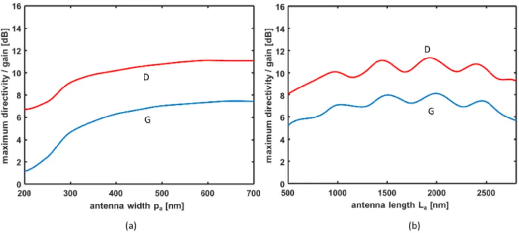
Fig. 5. (a) Maximum directivity (red curve) and gain (blue curve) of the single antenna coupled to the Si waveguide as a function of the antenna width pa. The antenna length is
La = 1500 nm; (b) Maximum directivity (red curve) and gain (blue curve) of the single
antenna coupled to the Si waveguide as a function of the antenna length Lafor pa= 700 nm. Figure 5(a) shows the maximum directivity D (red curve) and gain G (blue curve) of the single
antenna coupled to the Si waveguide as a function of the antenna width pa. In this case the antenna length is La= 1500 nm. The maximum directivity increases with the antenna width pa reaching the highest value D = 11.1 dB for pa= 700 nm.
Figure 5(b) shows the maximum directivity D (red curve) and gain G (blue curve) of the single antenna coupled to the Si waveguide as a function of the antenna length Lafor pa = 700 nm. The maximum value of the directivity D = 11.14 dB (gain G = 8.12 dB) corresponds to the length La= 2000 nm.
2.3. Optimization of the tilted Vivaldi antenna array
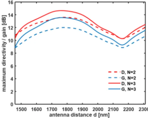
Once the geometrical parameters of the single antenna have been chosen (pa = 700 nm, La= 2000 nm, and Lin = 100 nm), the antenna array can be optimized by varying the number N of antennas and their mutual distance d. Fig. 6 shows the maximum directivity D (red curves) and gain G (blue curves) as a function of the distance d for a two- and three-element array (dashed and solid curves, respectively). Obviously, the minimum value of the distance d is geometrically constrained by the width pa. From Fig. 6, we can see that the curves with N = 3 are higher than the corresponding ones with N = 2, as expected from array behavior. Moreover, all the curves have a maximum around d = 1790 nm.
Fig. 6. Maximum directivity D (red curves) and gain G (blue curves) as a function of the distance d for a two- and three-element array (dashed and solid curves, respectively). The wavelength is λ = 1.55 µm and the length and the width of the antenna are La= 2000 nm
and pa= 700 nm.
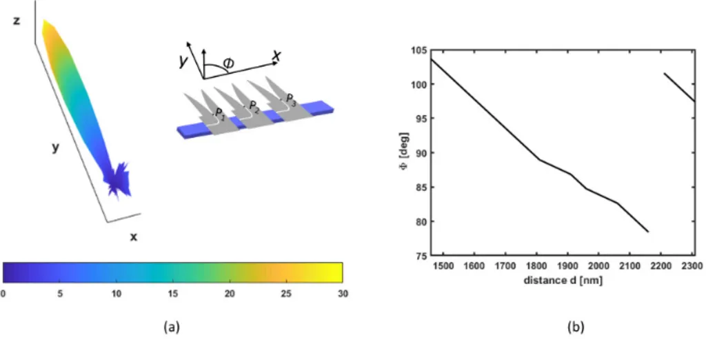
Figure 7(a) shows the three-dimensional diagram of the directivity D for an array with pa = 700 nm, d = 1790 nm, and N = 3. In this case, the maximum directivity and gain are, respectively, D = 14.59 dB and G = 13.47 dB. The scheme of the antenna array is also reported in Fig. 7(a) to better highlight the beam orientation Φ in the xy plane with respect to the array. In particular, in the considered case, the beam angle with respect to the x axis is Φ = 90◦, in agreement with what is expected from antenna theory for in-phase excitation of the antennas. In fact, we verified that all the antennas are in-phase for d = 1790 nm, by calculating the phase of the dominant Excomponent in input to the antennas (at the P1, P2, and P3dots in the scheme of Fig. 7(a)).
By changing their mutual distance d, a phase shift is induced between the antennas, thus influencing the maximum directivity D and gain G, as shown in Fig. 6. A further effect of the phase shift between the antennas is a tilt of the main beam in the xy plane. Fig. 7(b) shows
the tilt angle Φ of the main radiation beam as a function of the antenna distance d. The value Φ= 90◦corresponds to d = 1790 nm and, by changing the antenna distance from d = 1460 nm to d = 2160 nm, a steering of the main beam of about ∆Φ = 25◦ is achieved with a variation of the maximum directivity D of about 4 dB (see the red solid curve in Fig. 6 for N = 3). The phase shift depends on the propagation constants in the different sections of the array, (i.e. Si waveguide, hybrid Si-plasmonic waveguide in the coupler sections, and Au slot waveguide in the antenna region). The phase shift has, indeed, a periodic behaviour that is well reflected by the tilt angle Φ in Fig. 7 (b).
Fig. 7. (a) Three-dimensional diagram of the directivity D for an array with pa= 700 nm,
d= 1790 nm, and N = 3. The antenna array is also schematized to highlight the beam orientation Φ in the xy plane with respect to the array. (b) Tilt angle Φ of the main radiation lobe as a function of the antenna distance d for the same antenna array.
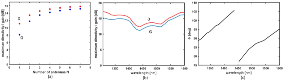
Figure 8(a) shows the maximum directivity D and gain G as a function of the number N of antennas, with pa = 700 nm and d = 1790 nm. By increasing the number N of antennas, the maximum directivity D and gain G increase, but the trend reaches saturation for N = 5 (where D= 15.46 dB and G = 14.70 dB). It is also worth noticing that the difference between D and G is lower for higher values of N. This translates, in natural units, in an increase of the radiation efficiency η = G/D with the number of antennas N. In fact, by increasing N, more power is coupled from the waveguide to the antenna array and, therefore, radiated in the surrounding medium.
A further aspect that is worth pointing out is the beam steering effect induced by the wavelength change of the input signal, which varies the phase shift between the antennas. Figs. 8(b) and (c) show, respectively, the maximum directivity D (red curve) and gain G (blue curve), and the tilt angle Φ of the main beam as a function of wavelength, for an antenna array with N = 5, pa= 700 nm, and d = 1790 nm. By varying the wavelength λ between 1500 nm and 1600 nm, a steering of the main beam of about ∆Φ = 10◦ is achieved with a variation of the maximum directivity D of about 3.7 dB.
3. Conclusion
In this paper we have proposed a plasmonic antenna array exploiting tilted Vivaldi antennas coupled to a silicon waveguide. The radiation characteristics of the array are suitable for on-chip wireless optical communication in the standard C (1530-1565 nm) telecommunication band.
Fig. 8. (a) Maximum directivity D and gain G as a function of the number of antennas N. (b) Maximum directivity D and gain G, and (c) tilt angle Φ of the main radiation lobe as a function of wavelength for an antenna array of N = 5 elements with pa = 700 nm,
La= 2000 nm, and d = 1790 nm.
Very compact arrays have been obtained (about 3.5 µm x 8.7 µm) thanks to a traveling wave feeding scheme, which allows for implementing compact and simplified feed networks (e.g. use of a limited number of directional couplers or signal splitters).
The design of the antenna array is performed, through the FDTD simulations, by firstly designing the single radiator coupled to the waveguide and, than, optimizing the array radiation characteristics. In agreement with the classical antenna theory, the plasmonic array radiation pattern mainly depends on the number of antennas N and on their mutual distance d. By increasing N, the directivity and the gain increase up to D = 15.46 dB and G = 14.70 dB for N=5, respectively. A further increase in the number of antennas does not give a significant improvement of the radiation characteristics (i.e less than 0.3 dB).
By varying the distance between the antennas, a tilt of the radiated beam is achieved owing to the consequent phase shift between the antennas. This beam steering effect allows for a tilt of the radiation diagram in the xy plane of about ∆Φ = 25◦, with a variation of the maximum directivity Dof about 4 dB. Similarly, for a fixed value of the distance d a beam steering of about ∆Φ = 10◦ can be obtained by changing the input signal wavelength between 1500 nm and 1600 nm. Funding
Ministero dell’Istruzione, dell’Universitá e della Ricerca (MIUR); PRIN 2015 (20155EABBC). Acknowledgments
Gaetano Bellanca acknowledges support from "Bando per l'acquisizione di strumenti per la ricerca di Ateneo - Anno 2015" of the University of Ferrara. V. Petruzzelli acknowledges support from "Risorse nel settore ricerca scientifica e tecnologica" of the Fondazione Puglia. G. Caló thanks Giovanni Magno and Béatrice Dagens, from C2N - Université Paris Sud, for fruitful discussions. The research was conducted in the framework of the project Galileo 2018 G18-625/ PHC Galilée 39622NL.
References
1. C. García-Meca, S. Lechago, A. Brimont, A. Griol, S. Mas, L. Sánchez, L. Bellieres, N. S. Losilla, and J. Martí, ”On-chip wireless silicon photonics: from reconfigurable interconnects to lab-on-chip devices,” Light Sci. Appl. 6, e17053 (2017).
2. Y. Yang, Q. Li, and M. Qiu, “Broadband nanophotonic wireless links and networks using on-chip integrated plasmonic antennas,” Sci. Rep. 6, 19490 (2016).
3. J. M. Merlo, N.T. Nesbitt, Y.M. Calm, A.H. Rose, L. D’Imperio, C. Yang, J.R. Naughton, M.J. Burns K. Kempa, and M.J. Naughton, “Wireless communication system via nanoscale plasmonic antennas,” Sci. Rep. 6, 31710 (2016).
4. R. G. Beausoleil, P. J. Kuekes, G. S. Snider, S. Wang, and R. S. Williams, “Nanoelectronic and nanophotonic interconnect,” Proc. IEEE 96(2), 230–247 (2008).
5. A. Shacham, K. Bergman, and L. P. Carloni, “Photonic networks-on-chip for future generations of chip multiprocessors,” IEEE Trans. Comput. 57(9), 1246–1260 (2008).
6. D. B. Miller, “Device requirements for optical interconnects to silicon chips,” Proc. IEEE 97(7), 1166–1185 (2009). 7. A. Biberman and K. Bergman, “Optical interconnection networks for high-performance computing systems,” Rep.
Prog. Phys. 75(4), 046402 (2012).
8. F. Gambini, S. Faralli, P. Pintus, N. Andriolli, and I. Cerutti, “BER evaluation of a low-crosstalk silicon integrated multi-microring network-on-chip,” Opt. Express 23(13), 17169–17178 (2015).
9. E. Fusella, and A. Cilardo, “Crosstalk-aware automated mapping for optical networks-on-chip,” ACM Trans. Embed. Comput. Syst. 16(1), 16.1 (2016).
10. M. Ortin-Obon, M. Tala, L. Ramini, V. Vinals-Yufera, and D. Bertozzi, “Contrasting laser power requirements of wavelength-routed optical NoC topologies subject to the floorplanning, placement and routing constraints of a 3D-stacked system,” IEEE Trans. Very Large Scale Integr. (VLSI) Syst. 25(7), 2081-2094 (2017).
11. C. V. Poulton, D. Vermeulen, E. Hosseini, E. Timurdogan, Z. Su, B. Moss, and M. R. Watts, "Lens-Free Chip-to-Chip Free-Space Laser Communication Link with a Silicon Photonics Optical Phased Array," in Frontiers in Optics 2017, OSA Technical Digest (online) (Optical Society of America, 2017), paper FW5A.3.
12. D. Kwong, A. Hosseini, J. Covey, Y. Zhang, X. Xu, H. Subbaraman, and R. T. Chen, "On-chip silicon optical phased array for two-dimensional beam steering," Opt. Lett. 39, 941–944 (2014).
13. C. T. Phare, M. C. Shin, J. Sharma, S. Ahasan, H. Krishnaswamy, and M. Lipson, "Silicon Optical Phased Array with Grating Lobe-Free Beam Formation Over 180 Degree Field of View," in Conference on Lasers and Electro-Optics, OSA Technical Digest (online) (Optical Society of America, 2018), paper SM3I.2.
14. A. Alù and N. Engheta, “Wireless at the nanoscale: optical interconnects using matched nanoantennas,” Phys. Rev. Lett. 104, 213902 (2010).
15. D. M. Solís, J. M. Taboada, F. Obelleiro, and L. Landesa, “Optimization of an optical wireless nanolink using directive nanoantennas,” Opt. Express 21(2), 2369–2377 (2013).
16. A. M. Ghanim, M. Hussein, M. F. O. Hameed, and S. S. A. Obayya, "Design considerations of super-directive nanoantennas for core-shell nanowires," J. Opt. Soc. Am. B-Opt. Phys. 35(1), 182–188 (2018).
17. G. Magno, A. Ecarnot, C. Pin, V. Yam, P. Gogol, R. Mégy, B. Cluzel, B. Dagens, "Integrated plasmonic nanotweezers for nanoparticle manipulation," Opt. Lett 41(16), 3679–3682 (2016).
18. M. Février, P. Gogol, A. Aassime, R.t Mégy, C. Delacour, A. Chelnokov, A. Apuzzo, S. Blaize, J. Lourtioz, and B. Dagens, "Giant Coupling Effect between Metal Nanoparticle Chain and Optical Waveguide," Nano Lett. 12(2), 1032–1037 (2012).
19. L. Yousefi, and A. C. Foster, “Waveguide-fed optical hybrid plasmonic patch nano-antenna,” Opt. Express 20(16), 18326–18335 (2012).
20. Y. Yang, D. Zhao, H. Gong, Q. Li, and M. Qiu, “Plasmonic sectoral horn nanoantennas,” Opt. Lett. 39(11), 3204–3207 (2014).
21. M. Saad-Bin-Alam, I. Khalil, A. Rahman, and A. M. Chowdhury, “Hybrid plasmonic waveguide fed broadband nanoantenna for nanophotonic applications,” IEEE Photonics Technol. Lett. 27(10), 1092–1095 (2015).
22. G. Bellanca, G.Calò, A. E. Kaplan, P. Bassi, and V. Petruzzelli, "Integrated Vivaldi plasmonic antenna for wireless on-chip optical communications," Opt. Express 25, 16214–16227 (2017).
23. G.Calò, G. Bellanca, A. E. Kaplan, P. Bassi, and V. Petruzzelli, "Double vivaldi antenna for wireless optical networks on chip," Opt. Quantum Electron. 50(6), 261 (2018).
24. A. Yariv, "Coupled-mode theory for guided-wave optics," IEEE J. Quantum Electron. QE-9 (9), 919–933 (1973). 25. G. Calò, A. D’Orazio, and V. Petruzzelli, "Broadband Mach-Zehnder Switch for Photonic Networks on Chip," J.
Lightw. Technol. 30, 944–952 (2012).
26. COMSOL Multiphysics,http://www.comsol.com/
27. Lumerical Solutions, Inc.http://www.lumerical.com/tcad-products/fdtd/
28. E. Palik, Handbook of Optical Constants of Solids (Academic, 1998).
29. P. B. Johnson and R. W. Christy, "Optical Constants of Noble metals," Phys. Rev. B 6, 4370 (1972). 30. R. E. Collin, Antennas and radiowave propagation (McGraw-Hill Book Company, 1985).