A
LMAM
ATERS
TUDIORUM–
U
NIVERSITÀ DIB
OLOGNAU
NIVERSITÀ DEGLIS
TUDI DIM
ODENA ER
EGGIOE
MILIAU
NIVERSITÀ DEGLIS
TUDI DIF
ERRARAU
NIVERSITÀ DIP
ARMAMASTER’S DEGREE IN
ADVANCED AUTOMOTIVE ELECTRONIC ENGINEERING
CLASS LM-29
SIMULATIONS AND AUTOMATED
TESTS OF BATTERY MANAGEMENT
SYSTEM CONTROL STRATEGIES
AND DIAGNOSIS ON HARDWARE IN
THE LOOP SYSTEM
Academic Year 2018/2019
Advisor:
Prof. Alessandro Chini
Co-Advisor:
Eng. Christian Pernaci
Candidate:
2
Summary
Abstract ... 4
1. Battery Managements System (BMS) ... 6
1.1. BMU: Battery Management Unit ... 7
1.1.1. Main Contactors and HV sensing ... 9
1.1.2. SOC and SOH estimation ... 10
1.2. CSC: Cell Supervisor Circuit ... 11
1.2.1. Cells Balancing ... 13
2. Hardware in the Loop System (HIL) ... 14
2.1. HIL hardware setup ... 16
2.1.1. DS1005 Processor Board ... 18
2.1.2. DS2210 Interface Board ... 18
2.2. BMS model-based design ... 19
2.2.1. Battery Cell Model ... 20
2.2.2. CAN and LIN communication ... 21
2.2.3. Control Desk ... 22
2.2.3. ETAS INCA & MDA ... 22
2.3. HIL Adequacy ... 26
2.4. Test Automation ... 28
3. Smart Booster Cells Emulator ... 31
3.1 State of Art ... 32 3.2 Hardware Configuration ... 33 3.2.1 Charging Net ... 35 3.2.2 Discharging Net ... 39 3.2.3 Control Net ... 40 3.3. Firmware configuration ... 41 3.3.1. Communication Protocol ... 42
3.4. Tests & Results ... 44
3
3.4.2. Frequency Response ... 46
3.4.3. Step Response ... 48
3.4.4. Output voltage ripple ... 50
3.4.5. Power-on ... 51
4
The aim of this master’s degree thesis is to describe the activities performed during a four months internship in Magneti Marelli Powertrain, Bologna. The role I covered in this period was Validation Engineer for Hybrid & Electric systems in Hardware in the Loop (HIL) environment, the main activity was to develop automated tests in python involving software and control strategies. Test automation feature is a crucial point in the development process of Electronical Control Units. In fact, it allows to perform non-regression test of every new software release in few hours’ time, despite manual test which are often time-consuming and for sure less precise and replicable. Moreover, automotive safety norm (ISO26262 [1]) obliges the Tier 1 to preserve test report of any product for 10 years and ensure the possibility of its exactly repeatability for the same amount of time.
The internship started with few weeks of formation and introduction to the work environment, where I had the occasion to familiarize with HIL environment and its main functionality involving test automation. The following step was to study the Battery Management system under analysis, starting from the single Li-ion battery Simulink model ending to the entire vehicle model needed to perform the desired tests.
During the internship period, I had the occasion to revisit the project of Cells Booster, a piece of power electronics hardware which emulates battery pack’s cells controlling their voltages. When Magneti Marelli started the production of the BMS system they designed internally a Cells Booster, unfortunately, its requirements where not fully known a priori being a completely new system for the company. The Cells Booster design helped control software developers in the initial stage of the project, the only thing
5
they needed were stable voltages and the possibility to evolve them at low frequencies. Nevertheless, when safety mechanism where introduced, it was clear that Cells Booster’s requirements where no more completely satisfied from the developed prototype.
Starting from the old Cells Booster electric schematic, with the precious help of Professor Alessandro Chini, we started developing a new concept of Smart Booster knowing, this time, the major requirements to follow:
• Cell’s voltage stability w.r.t. a broad frequency spectrum
• Digitalization of its communication protocol to save HIL resources • Modularization of the system for different application
• Passive & Active cell’s balancing features • Low overall cost
6
In order to ensure the correct and safe use of a Battery Pack, it is essential to provide a robust managements system. This litter should guarantee a series of features which controls the battery pack and, in case of critical situations, brings the vehicle back in safety condition. The BMS must acquire all cell’s voltages and maintain them balanced to avoid current flowing among them; moreover, it has to manage battery pack’s contactors, pre-charge relays and support the battery charger in its working phases. BMS’s responsibilities can be divided between software and hardware:
Software:
Hardware:
Voltages measurements Safety Circuitry Temperature acquisitions Main Contactor relays
Cells Balancing requests Pre-Charge relays
SOC & SOH estimation CAN/LIN communication
Pack State management Balancing actuation
The BMS is the only logical entity which is physically in contact with the High Voltage (HV) system. It receives commands from the body computer of the vehicle and checks whether these are admissible to be actuated. Starting from Key Off conditions, in order to reach the operational state, after having performed every safety check and sensed every cell’s voltage, the
BMS activates the Pre-Charge relay towards the inverter; when the inverter
voltage reaches around the 90-95 [%] of the battery pack’s voltage, Main
Contactor can be closed and the Operational State request is sent to the
inverter.
1. Battery Managements System
(BMS)
7
During Operational state, the BMS periodically asks for cell’s voltage data from the Cell Supervisor Circuits (CSC), measures the outgoing current to determine the SOC percentage and performs safety checks; these operations are usually repeated with a 10 to 100 [mS] periodicity.
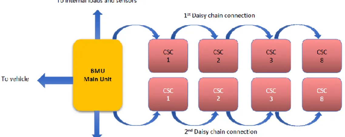
The BMS system can be seen as a core Battery Management Unit (BMU) and a series of CSCs, the first, is the system control core which integrates all the control and communication strategies coded via software. The CSCs circuits are the slaves of the system, they are dislocated among the battery pack sensing each cells’ voltage and temperature in different positions. The CSCs are connected in chain towards the BMU, their communication is usually isolated.
1.1. BMU: Battery Management Unit
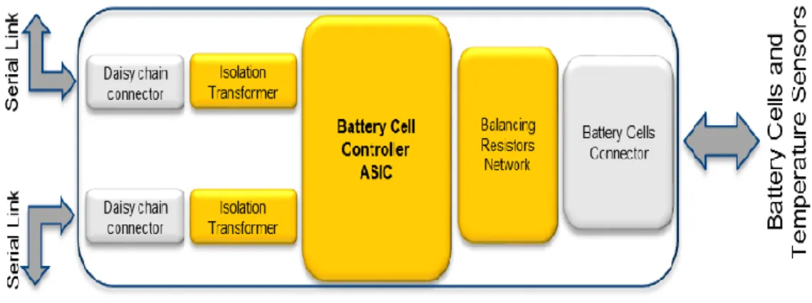
Figure 1: Battery Management Unit (BMU)
The Battery Management Unit is the central core of the system, it implements and integrates the communication protocol and the control strategies. The
BMU is connected towards CSCs with a dedicated isolated serial channel;
this line is used to receive voltage measurements of the cells and to command their balancing in the eventuality. The BMU presents a series of connectors:
8 • Vehicle Connector
• Internal loads and sensors • HV voltage sensor
• CSCs isolated link
The vehicle connector carries analog electric signals, digital
communication lines and a low voltage power source grounded to the
vehicle chassis. The communication protocols used are CAN and LIN.
There are four CAN lines working at different speeds: Vehicle-HS,
Vehicle-LS, a CAN-based sensor line and, finally, a Can Calibration
Protocol
(CCP)
line
used
in
the
deployment
phase.
Vehicle High-Speed line carries the most priority messages concerning
the propulsion module’s and vehicle control commands. The HS-CAN
line integrates the Unified Diagnostic Service (UDS) protocol,
accessible from the OBD vehicle connector. The UDS protocol allows
a unified management of the off-production maintenance; it allows the
interaction with the on-board diagnostic machine and, in some
applications, integrates the possibility of flashing a new software on the
ECU. The Low-Speed CAN is populated of non-strictly priority and
low-periodicity messages.
The BMU must maintain the battery pack’s temperature inside
pre-defined margin; these limits should be calibrated respect the chemists
of the cell. In fact, the exposure of the battery pack to extreme
temperature condition, either hot or cold, could be irreversible for the
battery cell’s health. The BMU must implement strategies either to cool
down or to heat up the battery pack. The cool down process is
performed using water pumps and a coolant circuit; pumps are activated
9
and controlled via LIN protocol, suitable for low bandwidth
applications. The heating up procedure can be performed activating the
cell’s balancing circuits or using external ad-hoc circuits.
1.1.1. Main Contactors and HV sensing
The Battery Management unit is provided of a series of isolated
operational amplifiers, those are needed to provide voltage
measurements of the main contactor’s poles avoiding the BMU to be in
contact with the HV system. This feature is essential in order to actuate
a proper charging stage of the inverter’s capacity before requesting the
contactor closing. The pre-charge circuit could be either a simple
resistor or a voltage converter, placed in parallel of main contactors. In
both cases the pre-charge is activated sensing the voltage across the two
poles; pre-charge is completed when those reach a similar potential,
thus, to avoid high currents flowing throw the contactor while closing.
10
Main contactors and relays activation coils are part of the Battery
Management unit; low sides switches are used for their activation.
High current and voltages tolerant contactors are often equipped with
an internal coil and an economizer circuit; this litter, manages and
reduces the power consumption of the contactor during the Operational
Stage.
1.1.2. SOC and SOH estimation
Important parameters to be estimated are the State of Charge (SOC) of the battery pack and its State of Heath (SOH); these, combined with other estimators, have direct impact on the control strategy actuated by the BMU.
The SOC estimation can be performed in different ways, the easiest one, is to integrate the current sourced by the battery pack divided by the total capacity of the pack. This approach is called the “Coulomb Counter”.
𝑆𝑂𝐶(𝑡) = 𝑆𝑂𝐶(𝑡 − 1) + ∫ 𝐼
𝐶𝑏𝑎𝑡 ∗ 𝑑𝑡 𝑡
0
This method suffers noise related errors, the current measure is often affected by disturbances; moreover, its measures should be performed continuously in order to solve the integral and the battery capacity should be measured in time. A more complex and accurate method for SOC estimation is the
Extended Kalman filter, more expensive in terms of computation rather than
the former. Kalman filtering allows to perform a precise estimation of the State of Charge of the battery being immune to current measurement noise.
The State of Heath (SOH) describes the decreasing of the performance due to calendar and cyclic aging. The SOH module implements three algorithms to estimate the health of the battery pack:
11
• Heuristic estimation by polynomial function • Internal resistance estimation
• Battery capacity estimation
The polynomial functions mentioned above are based on counters which increment when certain event take place; as the turning on phase of the vehicle or the battery pack reaching a certain temperature.
The estimates of SOC and SOH are the input of the State of Function (SOF) module which predicts the maximum instantaneous power deliverable from the battery pack. Finally, the BMU estimates the State of Life (SOL) of the battery. The input of the SOL module is the temperature history of the battery pack and its charge/discharge cycle number.
1.2. CSC: Cell Supervisor Circuit
The voltage sensing supervision circuit is composed by a transceiver, the
master, and a series of Cells Supervisor Circuits (CSC), the slaves of the
system, connected in daisy chain. The master is mounted on the BMU board acting as a transceiver, instead, slaves are placed on one or more boards placed as near as possible to the cells around the battery pack. In the following figure, a conceptual scheme of a CSC.
12
Figure 3: Cells Supervisor Circuit (CSC)
The Cells Supervisor Circuit integrates the balancing network and the connectors towards battery cells and temperature sensors; this module should be mounted in cell’s proximity in order to minimize the wiring. The CSC measures cell’s voltages with a series of Analog to Digital Converters (ADC), those can act in parallel minimizing the measurements timing; each CSC module can manage up to 14 cells.
The communication between the MCU and the CSC’s transceiver is held via
SPI protocol, instead, the downstream messages among CSCs are performed
using the isoSPI protocol; cheaper than the former in terms of wiring (two cables instead of four) and, primarily, used in order to have galvanically isolation among the devices by means of small transformer as the RJ45, typical of the Ethernet applications.
13
Figure 4: Battery Management System (BMS)
The conceptual schematic shown above figures the entire Battery Management System: a BMU and a chain of CSCs modules connected in daisy chain. Each CSC receives a command from the BMU and broadcasts it towards the next CSC in the chain, which will answer back with the required information. The BMU provides a double isoSPI chain connection, thus, to reduce the chain length and acquire voltage measurements in shorter times.
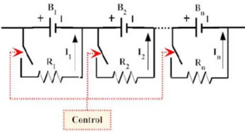
1.2.1. Cells Balancing
One of the fundamental tasks of the BMS is to ensure that every cell in the battery pack maintains the same voltage level of the others; this to avoid the presence of internal current flows among the cells; this phenomenon is likely to decay in avalanche irredeemably. In order to prevent the event previously described, a voltage potential balancing mechanism must be provided from
CSCs. This system can be either active or passive, in the first case, the
excessive charge of a cell is transferred, through isolated transformers or
DC/DCs, to other cells which are charge-lacking. The charge transmission
14
case instead, passive balancing, is a lossy process where the excessive charge is entirely dissipated on a resistor.
Figure 5: Cells passive balancing
Despite its lossy behaviour, passive balancing remains the most used commercial solution. State of art batteries and an accurate cells selection in the battery pack assembly, are prone to experience a common SOC and SOH level during their working life. For these reasons, cells’ balancing is usually likely to be needed only after a charging event.
The concept behind HIL system is the possibility to emulate the working environment of an ECU, being able to control and manoeuvre it. The model-based design of the environment is usually developed in MATLAB Simulink and then compiled for HIL computing board. The core can be either a
processor or an FPGA, it depends on the application and the relative
frequency of computation in order to correctly emulate the case environment.
2. Hardware in the Loop System
(HIL)
15
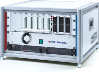
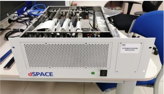
Figure 6: Hardware in the Loop (HIL)
The HIL system used in Magneti Marelli is from dSPACE [1], providing: simulation HW, model-based design IDE and a ControlDesk application for
Windows to control the entire system. The ECU is directly connected to the HIL and their signals process chain forms a closed loop: ECU’s outputs are
read from the HIL which processes and integrates them in order to elaborate the next environmental output, this will be the input of the ECU. In this way, it is possible to test a huge variety of ECU’s functionalities and working cases involving the entire vehicle. The simulator is equipped with all the communication protocols present in a vehicle (in the case study just CAN and
LIN), thus, it can emulate messages from all the other nodes of the system.
Hardware in the loop systems are nowadays a fundamental development tool for every component producer; it allows the arrival to the production stage with a far deeper coverage of any test case. In fact, once the model plant is developed, it is much easier to stress the system under analysis than the effort required to stress the real system.
The most important advantage gained using a simulator during software development, is the possibility of debugging the source code without leaving
16
the workstation. Moreover, a simulator avoids the difficulties of bringing the real vehicle in the conditions needed for the test, which are eventually extreme, like tests involving safety manoeuvres which need an experienced pilot driving on a circuit to be visible.
2.1. HIL hardware setup
HILs are usually customizable depending on the needs; it presents a
programmable power supply, a main processing core, communication peripherals and I/O boards, a Fault Injection Unit (FIU) and several load plates. The most expensive parts are the processing core, which directly impacts the simulation performance and sample timings, and the I/O adds-on depending on the complexity of the system to emulate (number of communication busses, number of ADCs or DACs and the number of general-purpose pins).
17
The core of the dSPACE platform can belong fundamentally to two families,
microprocessors or FPGA; the first family covers all the mostly used
application, instead, FPGA are used when timing constraint are excessively stringent like in powertrain application where the sample time needed is around 10 to 100 [µS]. The BMS’ HIL used in Magneti Marelli presents a
microprocessor core architecture, enough for the complexity of the running
model, and two interface boards managing:
• CAN communication
• ADC, DAC and PWM interfaces • Serial Peripherals
The HIL system designed in Magneti Marelli to emulate the environment of the Battery Management system presents:
• DS1005 Processor Board • 2 x DS2210 Interface Board • Cells Booster circuit
• Shunt emulator circuit • Main contactor
Despite the real main contactor is physically mounted inside the HIL, its poles are open circuited. Contactors presence is necessary in order to test the ability of the coil’s circuit to manage its closing. When the contactor is closed, the HIL feedback signal senses it and impose the DC bus model voltage value equal to the battery pack voltage, thus emulating the contactor close via software.
Farther, the shunt resistor is modelled; an electronic conditioning circuit manages the emulation of the battery pack’s currents, acting on the voltage potential across the shunt resistor.
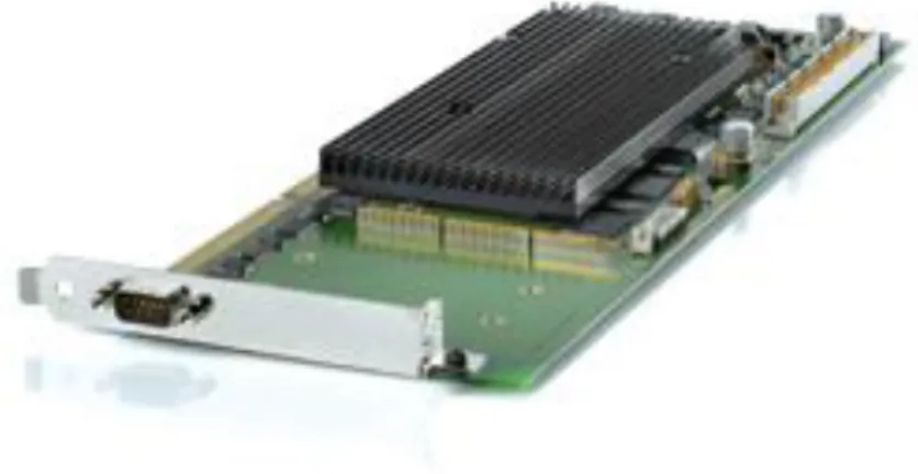
18
2.1.1. DS1005 Processor Board
The core of the Battery Management system’s HIL is a DS1005 processor core from dSPACE. Processor boards provide the computing power for the real-time system and acts as interfaces to the I/O boards and the host PC. The
DS1005 is the board of choice for applications with high sampling rates and
a lot of I/O capacity. High processing power plus fast access to I/O hardware with minimum latencies make dSPACE processor boards considerably faster than solutions based on commonly available PCs. The DS1005 features a PowerPC 750GX processor running at 1 [GHz]. The DS1005 is directly connectable to all dSPACE I/O boards via PHS and PHS++ bus.
Figure 8: DS1005 dSPACE Processor Board
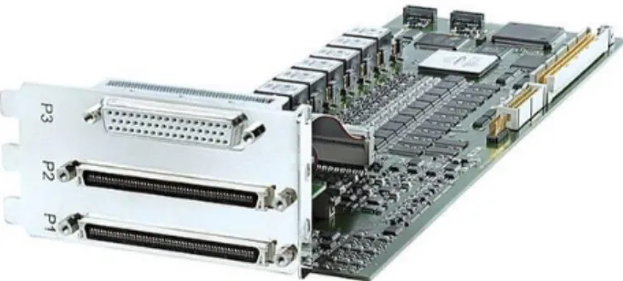
2.1.2. DS2210 Interface Board
The HIL is equipped with two DS2210 connected in parallel to cover all the interfaces needed to the system emulation. The DS2210 board does not provide LIN communication, thus, an external CAN to LIN converter is used; this receives packets from a dedicated CAN line and wraps them in LIN format.
19
Figure 9: DS2210 dSpace Interface Board
2.2. BMS model-based design
The model running on the dSpace platform is developed using MATLAB
Simulink environment, using ad-hoc adds-on from dSPACE managing the
communication towards the hardware. The toolchain provided from dSPACE guarantees a real time execution of the model, moreover, it allows to simulate other nodes of the system in terms of physical electrical signals and digital communication messages as CAN and LIN.
The model development process, at the first stage, is tested in an open loop configuration; the HIL produces signals which should be accurately checked before closing the loop with the ECU; in order to avoid undesired behaviours of the system and the possibility of irreversible damages to the equipment. Once the HIL engineer has performed all the needed open loop tests, the ECU is connected to the system and the closed loop control can be actuated.
In the following paragraphs the key points of the essential model for a BMS use case.
20
2.2.1. Battery Cell Model
In order to be effective, the HIL model should be calibrated with the components which will be present in the real vehicle, usually experimental data are analysed and sampled in look-up tables in order to simulate non-linear behaviours. Focusing on lithium cells, Magneti Marelli has internally developed a model which can be easily adapted to different cells coming from different producers. The experimental data needed for the model are the cell’s
SOC values related to the voltage, the capacity and the charge/discharge
characteristic of the cell at different current rates.
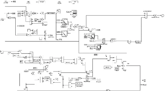
/
Figure 10: Lithium Cell model
Once the model is calibrated, it is able to accurately predict the behaviour of the cell and, thus fore, the entire battery pack characteristics evolution in time. The model can predict the voltage decrease related to a current absorption during the operational mode of the vehicle, as well, it can predict the temperature increase inside the battery pack related to a certain torque request.
21
2.2.2. CAN and LIN communication
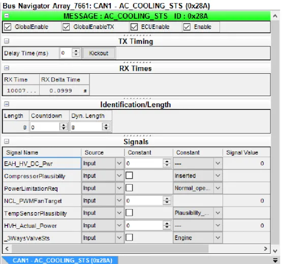
In order to simulate an entire vehicle, the communication towards the BMS from other nodes should be emulated directly from the HIL. During the configuration, it is possible to include in the project the CAN or LIN database, this file contains the ID of each node, their periodicity timings and the payload of the message. Once the “.dBc” or the “.ldf” database file is uploaded in the model, by means of the Bus Navigator, it is possible to set the payload of each message, either static or time varying. Farther, it is possible to configure the model of the HIL to acknowledge a specific message and answer consequently.
22
2.2.3. Control Desk
Once the vehicle model is developed on Simulink and compiled for the target simulator, it is possible to flash and control its variable using the Control
Desk tool from DSpace. This software allows the design of dedicated and
personalized layouts to control the different parts of the vehicle. In the BMS application different layouts where populated:
• Simulator power supply • Vehicle signals
• HV signals
• CAN communication • LIN communication
In the following figure, the layout controlling the cells’ emulator voltages.
Figure 12: Cells' Booster control layout, Control Desk
2.2.3. ETAS INCA & MDA
During the development phase of an ECU, the former is interfaced through
ETAS INCA, a tool which allows the real time acquisition of the ECU’s
23
software. Other important feature of INCA is the possibility to calibrate the
ECU at run-time without the necessity of compiling a new software. The
connection from the host pc to the ECU can be interfaced in two different ways:
• Can Calibration Protocol (CCP) • ETK
The CCP is a commercial protocol based on the CAN network, the ETK is an
Ethernet-based protocol. Despite the use of CCP is cheaper than the ETK,
the CAN-based protocol presents limits in terms of bandwidth of the acquisition and, more important, results weaker in the control of the ECU respect the litter protocol. The ETK communication, allows higher bandwidth and sampling rate; moreover, it is connected directly to the microcontroller with a separate power supply. Thus, with ETK it is possible to acquire variables from the microcontroller since its first clock cycle, allowing the monitoring of the software during the power on and power off phases. In the following figure, an example of ETK interfacing towards the ECU.
Figure 13: ETK connection scheme
The ETK protocol presents an ad-hoc power supply, interface towards the
ECU and microcontroller. In order to start the calibration with INCA, this tool
24
format) containing the addresses and information regarding the visible variables. The calibrations addresses must be declared and fixed in a dedicated RAM bank; INCA tool has a reference to the calibration area and creates a working copy of the former which is modifiable run-time.
Once the software is flashed on the ECU, it is possible to create different
INCA experiments where variables are selected and displayed as vectors,
tables, scalar or time oscilloscopes. It is possible to acquire variables with different sampling rates depending on the application and the role of the variable in the system. When the recording is activated, all the variables and calibration present in the experiment are saved in a “.mdf” file, which can be analysed either in python or using MATLAB. In the following figure, an example of INCA experiment.
25
Figure 14: INCA experiment
ETAS provides a graphical tool which can open and plot the “.mdf” file
recorded; the ETAS MDA (Measure Data Analyzer) measurement data analysis tool lets users visualize, further process, analyse, and document measurement data This tool is essential in the validation phase helping to have a visible trace of the variable’s evolution during a strategy actuation.
26
Figure 15: MDA (Measure Data Analyzer), ETAS
2.3. HIL Adequacy
In order to guarantee the efficiency and the required signal precision of the
HIL system, its adequacy must be tested with a certain periodicity. In the
specific case, it is regulated by safety norm ISO26262 that every signal considered as relevant in terms of safety, coming from the HIL towards the
ECU or vice versa, must be properly tested with a third observer: a calibrated
27
During the internship period in Magneti Marelli, I had the occasion to perform an HIL adequacy process; in the following figure, the experimental setup.
Figure 16: HIL Adequacy setup
The blue test box intercepts all the signals of the BMS’ connector towards the vehicle, the test box is used to connect oscilloscope’s probes to every connectors pin in the easiest way. The libraries used for the HIL adequacy are developed inside Magneti Marelli by the Tools & Methodology team. The adequacy procedures are automated using python, the user has to fill a calibration file containing information regarding: the variable under
examination on INCA, the shape of the signal produced by the HIL and conversion formulas for the three signals, in case they have different
physical units or scaling. Once the desired signal shape is defined, usually a slow ramp and a series of steps, the python code starts acquiring the signal read from INCA and from the oscilloscope, then, the post processing in
28
MATLAB overlaps the two acquisitions with the desired signal generated.
Tolerances bounds are defined, usually no more than 2 [% FSO], and an automatic report is made containing the three signals and the tolerance bands.
Figure 17: HIL Adequacy, Shunt Current Neg signal
2.4. Test Automation
The automatization of test allows a higher level of repeatability respect manual tests, moreover it allows fast and precise non-regression test. These litter tests are essential in the development of a new product; in fact, during the first stage of its design, it is important to demonstrate that every new software release has no impact on older features already tested. Non-regression tests, if automatized, could be executed during night time,
29
saving working hours of an employee. These tests should be executed at least every new software release to the client, as prove of having no regression respect the latest. For what concerns safety applications, the test’s reports must be saved for ten years’ time according to the ISO26262, moreover, the testing condition should be replicable for the same amount of time; which means that, the entire HIL system and the development ECU should be maintained unchanged for ten years’ time.
Non regression-test is a practice habitually performed in Magneti Marelli. Quality, functional, communication and safety test are firstly manually tested, then automatized using python coded libraries internally developed in Magneti Marelli. Those python objects manage the communication from the host PC towards:
• HIL’s processor board
• ECU via CCP or ETK, interfaced to the host PC with ETAS INCA • Diagnostic external tool
• MATLAB
Instances of those object are created in the main file and their methods are continuously called during the test acting on the system. The library concerning the control of the HIL is called “MMActHIL”, it integrates methods either to read and write model vars. The same happens for “MMApiINCA” capable of acquiring variables and modifying calibration values directly from the ECU, initializing the device and modifying its calibrations. An external diagnostic tool is needed to clear the error memory of the ECU and to read error patterns, also called Diagnostic Trouble Codes
(DTC); the related interface library is called “DiagTool”. Test scripts share a
common main file, which create the instances of the controlling objects and run the test script managing possible exception, printing out a test report and
30
its related variables acquisition in “.mdf” file format. In the case the test needs to check the evolution of the variables instead of their final value, the python script calls a MATLAB post-process loading the variables acquisition file. Test are grouped in Test Description (TD) containing different Test
Cases (TC), after every test execution an automated Test Report (TR) file is
saved on the host PC or server. The tool managing the above explained routine is the Test Launcher, developed inside Magneti Marelli.
Figure 18: Test Launcher, Magneti Marelli
Test Launcher is a basic graphical interface which manages the main file of
the test; once the test folder is selected, the launcher shows the relative TDs in columns. Test cases are selectable individually or in group, the launcher generates a test pattern and calls the main which performs the selected tests.
31
Once the main finishes the execution of a test case, it answers back to the launcher with a test result flag.
A Cells Booster is an active power load capable of emulating the voltage of a series of cell, thus, to simulate the behaviour of a battery pack in different conditions: charge, discharge, balancing and obviously in the static condition. This tool, built up in modules, gives the possibility to emulate the behaviour of a battery pack in various working conditions. Thus fore, it is possible to control the cells behaviour and check if the Electronic Control Unit acts correctly in the desired working scenario.
In static condition, the power absorption of a BMS HV system is strictly connected to the number of CSCs, even though, each of them absorbs around
20 [mA]; the current needed for the ADCs to perform measurements, the
communication and to perform safety checks. The pick of consumption happens during a passive balancing phase, when the Cells Booster must provide all the needed current, possibly without any voltage drop of the emulated cells. The voltage decreases compensation of a real cell voltage, following a current absorption, varies respect the type of cell used; thus, it should be managed via software in order to be calibrated without acting on its hardware.
32
3.1 State of Art
The cells booster used during the internship period in Magneti Marelli was internally developed by the Tools & Methodology team. The cells emulator is composed of a series of isolated converters to boost the voltage, and, a set of operational amplifiers to regulate it. The developed booster is low voltage powered; a few tens of [Watts] worst case. CSCs are connected in parallel to the same voltage source, thus, to maintain the simulator in low voltages range and in a limited space inside di simulator case. In terms of validation of a single CSC, this solution offers a complete validation process; even tough, the parallelization of the CSCs leads to a performance decay for the booster.
The voltage of every emulated cell is directly controlled with a DAC output pin of the HIL system, an extra reason for the parallelization of CSCs. The calibration of the cell’s voltage is performed using a PID controller with
INCA read voltage as feedback. HIL’s peripherals number has a direct impact
on the cost of the simulator, the analog control of the cells is not an efficient method in terms of resources usage.
The experimental activity held during the internship period, had the aim of developing a Cells Smart Booster to improve its previous version in term of:
• Modularity and Scalability with the application • Power Efficiency in static conditions
• Dimensions of the board • BOM cost
• Frequency response
• Active/Passive balancing managed • Digital Communication towards the HIL
33
3.2 Hardware Configuration
One of the desired achievements of this project was the modularity and scalability of the number of cells emulated; the idea was to produce a stock of this devices, which must be configurable for every eventuality. For this couple of reasons, it was important to maintain a compact design and a low cost of the bill of material.
The device proposed, emulates 16 cells, as the maximum number supervised by nowadays CSC components. Thus, the configuration of the cell emulator could easily follow the configuration of the battery pack cells’ supervisors. The Smart Booster is low voltage powered; 24 [V] input. This voltage was chosen in order to be compatible with standard working stations suppliers, and, in the meanwhile, as highest as possible in order to have the lowest switching currents in the power conversion. Smart booster can be configured to present a common ground among the devices; all powered by the same 24
[V] source and maintaining a maximum output voltage below the High
Voltage threshold, which overrun would involve the observation of a series of safety norms. The BMS acquires a series of voltage potential difference and does not recognize that the devices are grounded among them, thus performing a logic emulation of the battery pack. In case the HIL is situated in HV tolerant environment, Smart Booster boards could be powered singularly with isolated suppliers and connected in series via isolated communication transceivers, thus, reaching physically the real battery pack high voltage.The communication with the HIL has been implemented via
UART, however, it could be easily shifted on other peripherals depending on
the HIL resource’s availability. The HIL is connected to the first Smart Booster board, which receives all the commands, actuates cells voltage variation if required, and forwards the message to the second Smart Booster board. Assembling the system for the first time, an initial configuration
34
command must be sent to the chain of Smart Boosters, the first acknowledge itself as chain master and rules the ID assignment for the others. The IDs are permanently saved in the on-board flash memory of the MCU, until a new configuration command request from the HIL.
The solution designed for a single cell emulator presents a flyback converter feedback controlled. The isolated converter keeps a controlled voltage across its output capacitors while a Schottky diode prevents backwards currents; the discharge is activated via a power mosfet. The cell is emulated using a series of ceramic capacitors, which is charged or discharged throw a power circuit clocked at 50 [µS] periodicity. The design can be conceptually divided in three parts:
• Charging Net • Discharging Net • Control Net
Each part of the circuit has been accurately simulated using LTSpice tool, filtering the high frequency components with snubber nets. A first proto has already been produced and tested, it implements two cells in series controlled by a microcontroller; the board development was realized with Autodesk
Eagle, component’s footprint and placing was checked with the 3D export of
35
Figure 19: Smart Booster Prototype 3D render, Autodesk Fusion
3.2.1 Charging Net
As already mentioned, the charging net is implemented with a flyback isolated converter. The transformer was chosen to be 24 [V] tolerant with a turns’ ratio allowing an output voltage range from 2 to 6 [V]. Two different transformers were analysed, with different inductance value and consequently different currents picks. The proto board was developed in order to host both the transformers, to compare the simulated data with the experimental one before the realization of the 16 cells Smart Booster.
The flyback was controlled with an ad-hoc controller integrating the mosfet gate control, it’s current sensing shunt and an internal 20 [kHz] oscillator. The shunt resistor was properly tuned to compensate the action of the discharging net; when a constant voltage is required, the charging and the discharging net should sink and inject ideally the same amount of charge per clock period, thus, minimizing the ripple on the output. The flyback controller is actuated with a low voltage feedback command, which compares
36
the cell differential potential with the given target and activates the charging or the discharging net respectively. A Zener diode is placed in parallel to the output capacitors to prevent accidental voltage picks on the cell, thus, protecting the analog to digital converters of the CSCs circuits from an over-voltage.
Figure 20: Charging Net
In order to avoid high voltage picks and ripples, resulting in noise for the system, two snubbers [3] nets have been deployed. Their design is strictly related to the transformer stray inductance; snubber nets were dimensioned in simulations for both the transformers. The first and most important snubber net takes place between the drain and the source of the mosfet, due to the inductor current going rapidly to zero when the mosfet opens the circuit.
The resistor of the snubber net is essential to avoid the mosfet going in breakdown and eventually burn up; from the simulation, with a 24 [V] input source, the worst-case pick voltage applied on the mosfet is around 150 [V]. Despite, the role of the capacitor of the snubber is to act as a low pass filter, sinking the ripple across the mosfet. In the following figure, the simulation of the mosfet’s drain to source voltage.
37 Figure 21: Mosfet drain-to-source
voltage, no-snubber
Figure 22: Mosfet drain-to-source voltage, snubber present
In the first figure, the simulation of the drain to source voltage of the mosfet during the turning off phase. The ringing is properly damped using a snubber resistor equal to the characteristic impedance of the ringing.
𝑅 = 𝑍
𝑍 = 2𝜋𝑓𝑟𝐿
Where 𝑓𝑟 is the ringing frequency of the ringing and 𝐿 is the stray inductance of the transformer primary winding. The snubber capacitor, instead, is used to minimize the dissipation at the switching frequency, allowing the resistor to be effective at the ringing frequency. Thus, it is convenient to design the snubber capacitor to have the same impedance value of the resistor at the ringing frequency.
𝐶 = 1 2𝜋𝑓𝑟𝑅
38
The low pass RC filter design was initially designed simulating a non-ideal transformer with a worst-case stray inductance value found on the component’s datasheet. The passive component’s value was subsequently tuned with the experimental data from the first hardware proto.
The secondary snubber net is placed across the secondary winding diode, it follows the same design rule of the first. The secondary snubber filter design has less impact on the circuit robustness respect the first snubber net; however, it allows the use of a smaller and cheaper Schottky diode. The implementation of this secondary snubber net avoids the stressful behaviour of the diode, thus, remains a must in order to realize a robust and long-lasting power circuit. In the following figure, the secondary winding diode forward voltage.
Figure 23: Schottky diode forward voltage, no-snubber
Figure 24: Schottky diode forward voltage, snubber present
39
As we can see from the first figure, the diode suffers a ringing reversed biased voltage due to the transformer activity. This behaviour could possibly shorten the diodes working lifetime. The same simulation was repeated with the presence of a snubber RC filter with the effects shown in Figure 24.
3.2.2 Discharging Net
As previously mentioned, a single cell of a battery pack is emulated with a series of isolated ceramic capacitors. If the target voltage goes above the cell voltage, the control net pushes the feedback signal to the high logical value; the charging net is deactivated, and the discharge circuit starts sinking current from the cell.
Figure 25: Discharging Net
The discharge circuit consist in a P-channel mosfet and a resistor in series, it is controlled with an optical coupled mosfet. In this way it is possible to actuate the discharging circuit of every battery cell of the series, the highest voltage terminal of the Smart Booster can reach 80 [V] being 16 cells in series. The mosfet gate is controlled with a series of diodes instead of the pull up resistor, therefore, to stabilize the mosfet gate to source voltage respect the voltage range admissible by the emulated cell.
40
3.2.3 Control Net
The Analog Control net is entirely 24 [V] powered, it takes as input the potential difference of the cell’s terminals and gives as output a logic low low level to activate the charging circuit or, a logic high level to power the discharging net. The first module of the Analog Control Net is a differential amplifier which compute the difference between the cell’s poles voltages; this device must present an elevated common mode rejection in order to work at 80 [V] worst condition.
Figure 26: Analog Control Net
The second part of the net presents a logical comparator, it takes as input the cell differential potential and the target signal of the cell. This component presents an internal Bipolar Junction Transistor (BJT) which shorts the feedback output voltage to ground in case 𝐼𝑁− > 𝐼𝑁+ [V] or, vice versa leaves it floating; in the litter case, the feedback voltage is managed through a voltage divider. The target voltage is provided by the Digital Control Net, which, despite the analog net, is low voltage powered.
The Digital Control Net presents a power supply chain, a first Buck Switching
Converter and a couple of low-dropout (LDO) regulators supplying the MCU
and the DAC respectively. The target voltage signal is managed using an external Digital to Analog (DAC) module, which communicates via the Inter
41
Integrated Circuit (I2C) serial protocol with the Micro Controller Unit (MCU), the master device of the board. The Smart Booster is equipped with
an MCU STM32-F0 series from STMicroelectronics.
3.3. Firmware configuration
Smart Booster’s firmware is implemented using STM32 [5] Hardware
Abstraction Layer (HAL) libraries, the peripherals configuration has been
managed with STM32 CubeMX software. Follows a list of the peripheral used:
• 2 x UART • 1 x 𝐼2𝐶 • 4 x ADC • 6 x GPIO
The 𝐼2𝐶 peripheral of the microcontroller is connected in parallel to four external DACs modules, activated individually with a chip select signal driven directly from di microcontroller GPIOs. The 𝐼2𝐶 protocol manages
DACs’ initial configuration at power on, and commands them to actuate the
required voltages on their outputs. The drivers used for the communication between the MCU and the external DAC where found open source and wrapped for their use with the HAL libraries.
As previously mentioned, the DAC module used presents an internal
EEPROM storing the latest output configuration of each channel, thus, to
recover their last state in case of a power cycle. 𝐼2𝐶 command can either update the EEPROM voltage value or leave it unchanged and update just the output register. If the command needs to write the DAC memory, the MCU
42
must wait until its completion, sensing the ready pin of the component with its ADC peripheral.
The communication with the extern of the Smart Booster is held via the
UART peripheral; one for the input command and one for the output,
imitating the isoSPI chain followed by CSCs.
Figure 27: Smart Booster prototype
The HIL communicates with the first Smart Booster via its UART IN port, the message is elaborated and forwarded to the next Smart Booster in series via its UART OUT port. In this way the booster results to be modular and scalable for different application uses.
3.3.1. Communication Protocol
The communication protocol implemented is based on UART and present a three bytes length. The first Smart Booster receives all the commands and forwards them only if necessary, the same happens for the other modules in the chain. The first time that a series of Smart Boosters are mounted together,
43
a firmware initialization command must be sent from the HIL containing the number of Smart Boosters connected in chain; during this phase the first booster understands to be the master of the chain and takes the 0-ID, storing it into its flash memory, then it sends the initial command to the second booster which takes the 1-ID and the procedure continues until the last Smart Booster. The initial command from the HIL is followed by a series of messages, one for each booster, containing the number of cells to be emulated by the different IDs. Once this operation is completed the Smart Booster system is set up and the working phase can start.
Byte: 0 1 2
Command Booster ID Cell Num target-MS target-LS
The byte 0 contains the command type:
• Initial command • Broadcast command
• Multi/Single cell write command • Flash involved or not
• Booster ID
Receiving this first byte the microcontroller is already able to distinguish if the message should be forwarded or just actuated. The last two bytes of the command contain the target voltage required to the cell, either in single or multi cell write command, and the cell number.
44
3.4. Tests & Results
A first prototype of the Smart Booster was produced and soldered inside
Magneti Marelli, the proto version presents only two cells in series, thus, to
enable the test of all the functionalities of the system. The proto board was designed to work with two different types of transformers, in order to compare these two as done in the first simulation stage. Two proto boards where mounted with different transformers placed respectively on the top and bottom side of the board.
The experimental results proved that the best-choice transformer implied the biggest inductance value possible; the quantity of energy stored in the transformer is directly proportional to its inductance value. This choice implies that the circuit is subject to lower currents respect the first case, resulting in lower noise on the signals.
Once the initial testing phase was terminated and the board were acting in the desired way, two Smart Booster prototypes were connected in series in order to test the firmware command forwarding feature.
Figure 28: Smart Booster prototypes chain
The master booster of the chain is the board on the left, connected directly to the HIL’s UART peripheral; this first board forwards commands to the
45
second. The ground of the second Smart Booster is connected to the second cell of the first, obtaining four cells in series.
3.4.1. Safety mechanism tolerance
The cells booster formerly designed presented an elevated output impedance value, thus, resulting in non-tolerable voltage spikes when safety mechanisms were activated from the BMS board; his strategy controls a resistor in parallel to the cell in other to verify its presence. Moreover, the high output impedance value causes a voltage drop during the balancing phase. In the following figure, the comparison of the output voltage of the old booster and the newly designed.
Figure 29: Cells Boosters output voltage comparison, constant target. Green trace: Smart Booster output voltage
46
The stability of the output voltage was obtained minimizing its output impedance value using an isolated boost converter. The voltage drop during the balancing phase is cancelled by the use of an analog closed loop feedback control signal activating the charging/discharging nets.
3.4.2. Frequency Response
The initial requirement relative to the frequency response of the Smart
Booster was the possibility of reaching a 10 [Hz] chasing of the target
variation. The test was held with no loads, neither active nor passive balancing were present.
The frequency response of the Smart Booster was obtained experimentally setting a sinusoidal target voltage and varying its frequency. The signal externally sourced with a generator presents:
• V_Offset 3.5 [V]
• V_PickToPick 3.0 [V]
In the following figure, an oscilloscope acquisition with 50 [Hz] input target. The channel 1 (C1), on yellow, is connected directly to the signal generator,
channel 2 (C2), in green, is the output of the first cell of the Smart Booster
prototype. In the bottom of the figure, pick-to-pick voltage and frequency measurements of the two channels.
47
Figure 30: Smart Booster, Sinusoidal target, 50 [Hz] CH1: Yellow trace. Input signal. [1V/div ; 10mS/div ; 0 Pos] CH2: Green trace. Output signal. [1V/div ; 10mS/div ; -1 Pos]
From this figure it is possible to observe that the output signal of the Smart
Booster is perfectly able to follow the target one, the two measured pick-to-pick voltages are equal, thus, unitary magnitude of the frequency response at 50 [Hz].
Repeating this experiment varying the frequency of the target’s sinusoidal signal it is possible to obtain an experimental frequency response of the system. The resulting magnitude is the ratio between the target pick-to-pick voltage and the relative booster output voltage.
48
Figure 31: Smart Booster, Frequency Response
This figure confirms that the frequency response requirement is fulfilled. The Smart Booster can perfectly emulate the behaviour of a cell varying until 60
[Hz] circa.
3.4.3. Step Response
The system was tested with a step target signal in order to verify its timings characteristic in the worst-case scenario. The test was held with no loads, neither active nor passive balancing were present. The step was generated using:
• V_Offset 3.5 [V]
49
Figure 32: Smart Booster, Step Response. CH1: Yellow trace. Target signal. [1V/div ; 5mS/div] CH2: Green trace. Output signal. [1V/div ; 5mS/div]
This test revealed that the weakest part of the system is the discharging circuit, this was dimensioned in order to minimize the ripple of the output signal; allowing the discharge net to sink more current would imply an higher ripple which will worst the system respect its fundamental state with constant target. The system can decrease its voltage from 5 [V] to 2 [V] in
6 [mS]; the real working scenario of a cell is around the half of this range,
thus, taking circa the half of the time. It is possible to confirm that the requirements relative to the logical emulation of a battery pack are fulfilled by the Smart Booster.
50
3.4.4. Output voltage ripple
In the following figure an acquisition from ETAS INCA of the first cell of the Smart Booster. The target is a constant voltage, thus, focusing on the output voltage ripple; as result, the litter results to be lower than 1 [%] FSO.
51
3.4.5. Power-on
The firmware is configured to save a 3.5 [V] as outputs of the DAC modules, thus, setting this voltage as target at the power on of the board. The test was held with no loads, neither active nor passive balancing were present. The test was performed triggering the power on phase of the fourth cell. The system results to be turned on after less than 3 [mS] fulfilling the power on requirement of 10 [mS].
52
[1] dSPACE. Retrieved from
https://www.dspace.com/en/inc/home/products/systems/ecutest.cfm
[2] ETAS. INCA & MDA. Retrieved from
https://www.etas.com/en/products/inca.php
[3] Flyback Converter Snubber Design. (2005). Dr. Ray Ridly.
[4] International Organization for Standardization . (2011, November 11). ISO26262. Road vehicles – Functional safety.
[5] STMicroelectronics. Retrieved from https://www.st.com/en/embedded-software/stm32cube-mcu-mpu-packages.html