0257-8972/03/$ - see front matter䊚 2002 Elsevier Science B.V. All rights reserved. PII: S 0 2 5 7 - 8 9 7 2 Ž 0 2 . 0 0 7 7 5 - 2
Dry turning of alumina
yaluminum composites with CVD diamond coated
Co-cemented tungsten carbide tools
Riccardo Polini *, Fabrizio Casadei , Pierangelo D’Antonio , Enrico Traversa
a, b a aDipartimento di Scienze e Tecnologie Chimiche, Universita di Roma ‘Tor Vergata’, Via della Ricerca Scientifica, 00133 Rome, Italy
a `
Centro Sviluppo Materiali S.p.A., Via di Castel Romano 100, 00100 Rome, Italy b
Received 16 April 2002; accepted in revised form 18 October 2002
Abstract
Triangular(TPGN 160308) WC–6 wt.%Co inserts having different average grain sizes (1 and 3 mm) were submitted to surface
roughening either by wet etching with Murakami’s reagent or by a heat treatment in the hot filament chemical vapour deposition
(HFCVD) reactor. The heat treatment was performed in a monohydrogen-rich atmosphere at substrate temperatures as high as
1000 8C. Scanning electron microscopy and energy-dispersive spectroscopy showed that this pre-treatment led to surface roughening of the as-ground inserts and to a lower surface Co concentration. Prior to deposition, all inserts were etched with an acid solution of hydrogen peroxide. Diamond coatings were deposited by HFCVD. The coated inserts were tested by dry machining of aluminum–matrix composite (Al–10%Al O ) bars. Turning test results indicated that a proper combination of2 3 substrate pretreatment and microstructure can significantly improve tool life.
䊚 2002 Elsevier Science B.V. All rights reserved.
Keywords: Hot filament chemical vapour deposition; Tungsten carbide; Diamond; Dry turning of MMC materials; Scanning electron microscopy
1. Introduction
Metal–matrix composites (MMCs) are a class of materials consisting of a high-performance non-metallic phase, incorporated into a conventional engineering material. This is a monolithic alloy and the reinforce-ment may be: graphite, silicon carbide (SiC), boron, aluminum oxide(Al O ), or refractory metals w1x.2 3
Aluminum-based MMCs, reinforced with either SiC or Al O , have attracted the attention of automotive2 3 companies, dealing with components such as brake disks and drums, pistons, and cylinder liners. At present, brake components with improved thermal stability, ther-mal conductivity, and wear resistance, are in an advanced state of development w2x. However, both the extreme short life and poor performance of conventional carbide cutting tools cause high costs for MMCs machining. Reasonable tool life can be obtained only by using more expensive polycrystalline diamond (PCD) products.
*Corresponding author. Tel.: 4414; fax: q39-6-7259-4328.
E-mail address: [email protected](R. Polini).
Nevertheless, PCD tools cannot be made with complex cutting edge geometries. Therefore, diamond films deposited by chemical vapour deposition (CVD), due to their outstanding wear resistance, look very promising in the important market of difficult-to-machine materials w3–6x, including the MMCs.
The most suitable substrate material for producing diamond coated tools is cobalt-cemented tungsten car-bide (WC–Co). However, the cobalt binder, which provides additional toughness to the tool, is hostile to diamond adhesion w7–9x. As a consequence, it is impos-sible to deposit adherent diamond coatings onto untreat-ed WC–Co tools unless surface cobalt is removuntreat-ed. Moreover, a significant factor for the adhesion of CVD diamond to WC–Co substrates is the mechanical inter-locking occurring at the coating–carbide interface w10x. Therefore, a substrate pretreatment, for both significantly reducing the surface Co concentration and achieving a proper interface roughness, represents a crucial step in the coating process. Its effectiveness in increasing adhe-sion and attaining the desired functional properties of WC–Co coated parts is also influenced strongly by substrate microstructure.
Table 1
Chemical compositions and properties of WC–Co substrates
WC–Co Nominal composition Density Hardness Transverse Coercivity
grain size (wt.%) (gycm )3 (HV10) strength(MPa) (Oe)
1 WC–5.8%Co–0.2%VC–0.2%TaC 14.91 1740 3350 275
3 WC–6%Co 14.96 1445 3538 135
Table 2
Chemical and thermal pretreatments of WC–Co substrates
M10 10 min etching with Murakami’s reagent q10 s etching with H O qH SOa b 2 2 2 4 M1 1 min etching with Murakami’s reagent q5 s etching with H O qH SOa b
2 2 2 4
T9 3 h heat treatment in the HFCVD reactor, using a 0.5% vyv CH yH atmosphere4 2 (filament temperatures2350 8C, substrate
temperatures1000 8C, total gas pressures9 Torr)q10 s etching with H O qH SOb 2 2 2 4
T18 1 h heat treatment in the HFCVD reactor, using a 0.5% vyv CH yH atmosphere4 2 (filament temperatures2350 8C, substrate
temperatures1000 8C, total gas pressures18 Torr)q10 s etching with H O qH SOb 2 2 2 4
T36 3 h heat treatment in the HFCVD reactor, using a 0.5% vyv CH yH atmosphere4 2 (filament temperatures2350 8C, substrate
temperatures1000 8C, total gas pressures36 Torr)q10 s etching with H O qH SOb 2 2 2 4 10 g K wFe(CN) xq10 g KOHq100 ml of water.
a
3 6
3 ml 96 wt.% H SO q88 ml 40% myv H O .
b
2 4 2 2
In this work, we have studied the effect of substrate pretreatment and grain size on the wear resistance of diamond coated WC–Co inserts in the dry turning of aluminayaluminum composites.
2. Experimental details
2.1. Substrates and pretreatments
Two sets of WC–Co (WC–6 wt.%Co) cutting inserts (TPGN 160308) with fine (1 mm) and medium (3 mm) average grain sizes, supplied by F.I.L.M.S. SpA(Anzola d’Ossola, Italy), were used as substrates. Nominal chem-ical compositions, density, hardness and coercivity of these sintered materials are given in Table 1.
The as-ground substrates were rinsed with acetone and ethanol. Since adhesion strength may be improved by increasing the interfacial area between film and substrate w10x, the inserts were chemically or thermally pretreated under the conditions listed in Table 2. The chemical etching (M) comprised a two-step procedure. A first etching, using Murakami’s reagent (10 g K wFe3 (CN) xq10 g KOHq100 ml of water), was6 carried out for 1 or 10 min in a ultrasonic vessel, followed by rinsing with deionized water. The second etching step was performed using an acid solution of hydrogen peroxide(3 ml 96 wt.% H SO q88 ml 40%2 4 myv H O2 2), for 5 or 10 s, to remove Co from the surface. The substrates were then rinsed again with deionized water. The thermal pretreatment (T) first comprised 1 or 3 h heat treatment in the hot filament chemical vapour deposition (HFCVD) reactor w11x, using a 0.5% CH4yH atmosphere and 1000 8C substrate2 temperature. The total pressure was in the 9–36 Torr range and the gas phase was activated by a tantalum filament heated up to 2350 8C, as measured by a
two-colour pyrometer (Land Infrared model RP 12). Under these conditions, no diamond crystals nucleated at the substrate surface, likely due to both the low methane concentration and the high substrate temperature. Fol-lowing the heat treatment, the inserts were etched for 10 s with the H O qH SO solution and rinsed with2 2 2 4 deionized water.
The substrates were marked with a number(either 1 or 3, according to the average grain size) followed by a capital letter (M or T) with a number according to the type of pretreatments, as listed in Table 2.
All the substrates were analyzed by scanning electron microscopy (SEM, Leica Cambridge Stereoscan 360, with LaB source6 ), and energy-dispersive spectroscopy (EDS, Link eXL II).
2.2. Diamond deposition
Process conditions, indicated as A, ensuring a depo-sition rate as high as 1.5"0.2 mmyh, were employed. The gas phase was a mixture of hydrogen and methane with a CH4yH volume ratio fixed at 1.5%, activated2 by a carburized Ta filament (1 cm area) held at 23002 8C and at 8 mm from the substrate surface. The total pressure of the gas mixture in the reactor was 36 Torr with a flow rate of 300 standard cm3ymin. Substrate temperature was 780 8C and deposition time either 8 or 16 h. Other process conditions (indicated as B) were used to coat one fine-grained substrate, pretreated according to the M10 procedure. These conditions gave rise to a slower deposition rate, down to 0.55"0.05 mmyh. In this case, both a lower methane concentration (0.5% by volume) and a lower filament temperature (2180 8C) were used.
The CVD coated inserts are listed in Table 3, as well as the thickness of the diamond coatings.
Table 3
CVD diamond coated WC–Co inserts
Insert Substrate Pretreatmenta Process Deposition Film
grain size(mm) conditionsb time(h) thickness(mm)
1M10_A8 1 M10 A 8 11 1M10_A16 1 M10 A 16 23 1M10_B40 1 M10 B 40 24 3M10_A16 3 M10 A 16 23 3M1_A16 3 M1 A 16 24 3T9_A16 3 T9 A 16 28 3T18_A16 3 T18 A 16 23 3T36_A16 3 T36 A 16 26 According to Table 2. a
A, 1.5"0.2 mmyh deposition rate(1.5% CH yH ); B, 0.55"0.05 mmyh (0.5% CH yH ).
b
4 2 4 2
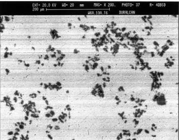
Fig. 1. SEM micrograph showing the typical microstructure of a 6061 Al alloy reinforced with 10%Al O2 3(W6A.10A.T6 by Duralcan).
Fig. 2. SEM micrograph showing the surface morphology of the ground rake face of as-received WC–Co inserts.
Diamond films were characterized by SEM and micro-Raman spectroscopy. micro-Raman measurements were per-formed in back-scattering geometry at room temperature by using a Dilor XY triple spectrometer equipped with a liquid nitrogen cooled charge coupled device detector and an adapted Olympus microscope. The spectra were excited with an Arq laser (514.5 nm, 3 mW) focused onto a spot of 1 mm in diameter. The scattered light was not analyzed in polarization. The spectral resolution was 0.5 cmy1. The lines of a neon lamp were used for frequency scale calibration. Diamond film thickness was measured by infrared interferometry, using a BioRad FTS 40A Spectrometer.
2.3. MMC machining: turning tests
In order to check their cutting performance, the diamond coated inserts were used to machine W6A.10A.T6 MMC bars(6061 Al alloy reinforced with 10% Al O2 3) supplied by Duralcan (Canada). Fig. 1 shows the typical microstructure of the W6A.10A.T6 MMC material. The workpiece size was 230 mm in diameter and 480 mm in length. Prior to the turning tests, a 1 mm thick external layer of the workpiece was removed due to the lower density of the Al O particles,2 3 as evidenced by SEM analysis of the bar cross-section.
Dry turning tests were performed using a SAG 210 Graziano machine and the triangular inserts were installed on a Sandvik CTGPR2525K16 tool holder. The following cutting conditions were employed: cutting speed,v s480 mymin; feed rate, fs0.4 mmyrev; depthc of cut, DOCs1.5 mm.
The flank wear of the inserts was estimated by SEM at selected time intervals (10 and 15 min). Prior to SEM analysis, the inserts were cleaned in a 6 M NaOH solution to remove Al alloy from the cutting edge.
For comparison purposes, PCD(Polydiam 4 by Cafro S.r.l., Italy) inserts with the same geometry were also tested.
Fig. 3. SEM micrograph showing the typical flank surface morphol-ogy of as-received WC–Co inserts.
Fig. 4. Surface morphologies of 1 mm-(panel a) and 3 mm-grained (panel b) WC–Co substrates chemically pretreated using Murakami’s
reagent(10 min etching time) and H O qH SO solution (10 s etch-2 2 2 4 ing time).
Fig. 5. Surface morphology of 3 mm-grained WC–Co substrates sub-mitted to 1 min etching with Murakami’s reagent and 5 s etching with H O qH SO solution.2 2 2 4
3. Results and discussion
3.1. Characterization of pretreated substrates
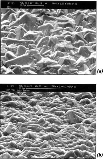
Fig. 2 shows the typical smooth surface of the rake face of an as-ground insert. Co concentration measured by EDS was 5.0"0.2 wt.%. Fig. 3 shows the flank morphology of 3-mm grained substrates before any pretreatment. The micrograph shows the typical micro-structure of as-sintered WC–Co inserts and indicates that the flanks of as-received specimens were not sub-mitted to any grinding treatment. A similar flank mor-phology was observed for fine-grained substrates, the sole difference being the average size of WC grains.
Fig. 4 shows the surface morphologies of M10-pretreated substrates with different WC grain sizes. Both the rake face and the flank exhibited the same morphol-ogy. The M10 pretreatment induced surface corrugation due to carbide chemical attack by the alkaline solution of potassium ferricyanide. After the first etching step, af2.5 mm thick WC surface layer was removed, as determined by substrate weight loss w12x. This weight loss was independent of the substrate grain size, thus confirming previous data from our laboratory w11–13x. The second etching step with H O qH SO did allow2 2 2 4 the reduction of surface Co concentration to a level below the detection limit of the EDS technique. Fig. 5 shows the surface morphology of a 3 mm grained substrate submitted to the M1 pre-treatment. After the first etching step, the thickness of the removed WC surface layer was approximately 0.2–0.3 mm, as esti-mated by the insert weight loss. It is worth noting that the surface roughness produced by 1 min etching with Murakami’s reagent in the ultrasonic vessel was com-parable to the one obtained after 10 min etching (com-pare Fig. 5 to Fig. 4b). Therefore, a longer etching time
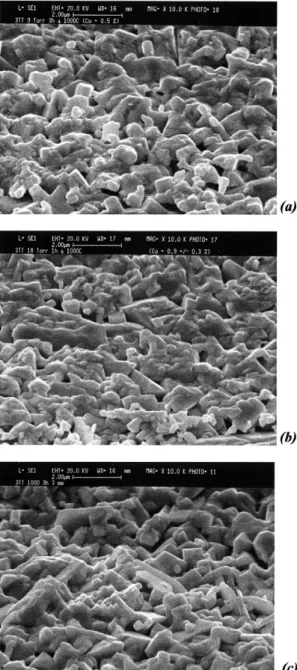
Fig. 6. Rake face morphologies of 3 mm-grained WC–Co substrates submitted to thermal pretreatment in 0.5% CH4yH atmosphere using2 different total gas phase pressures and treatment times: (a) 1 h, 9
Torr;(b) 1 h, 18 Torr; (c) 3 h, 36 Torr (substrate temperatures1000 8C; filament temperatures2350 8C).
Fig. 7. Typical flank morphology of 3 mm-grained WC–Co substrates submitted to thermal pretreatment.
with the alkaline solution of potassium ferricyanide led only to a deeper removal of surface WC and not to a significant increase of surface roughening. Moreover, the surface Co concentration was again below the EDS detection limit, even if the duration of the second etching step with H O qH SO was 5 s only.2 2 2 4
Fig. 6 shows the surface morphology of the rake face of 3-mm sized substrates submitted to T9(panel a), T18 (panel b) and T36 (panel c) thermal treatments. These treatments induced surface corrugation of the rake face, but through a different mechanism from the one
observed when Murakami’s etching was performed. In fact, as already discussed in a previous paper and evidenced by X-ray diffraction data w11x, the T-pretreat-ment led to the recrystallization of the outermost layer of WC grains, strained by the grinding treatment. This surface recrystallization of WC is attributed to local high temperatures caused by both H-atoms recombina-tion at the substrate surface and release of the stored strain energy. Both these effects could have determined the surface temperature much higher than that measured by the thermocouple (1000 8C). Panels a–c of Fig. 6 also show that similar surface morphologies were observed after 1 h thermal treatment at 18 Torr total pressure as well as after 3 h at 36 Torr. Following the T9, T18 and T36 treatments, the surface Co concentra-tions revealed by EDS were in the 0.5–0.9 wt.% range. This fact indicates that the high surface temperatures developed during the thermal treatment caused binder phase removal either by Co direct evaporation or for-mation of volatile compounds. However, in order to further reduce the surface Co level, it was decided to etch the thermal treated substrates with H O qH SO2 2 2 4 prior to deposition. After this wet etching step, surface Co concentration was below 0.2 wt.%.
Fig. 7 shows the SEM micrograph of the flank of 3-mm grained substrates after the T-pretreatment. It is worth noting that the thermal treatment induced different changes in the WC grains which were not submitted to the grinding treatment. In fact, due to the absence of strain-related defects, the thermal treatment alone could not activate a nucleation and growth mechanism of new, stress-free grains. Therefore, the sole observed effect was the growth of WC grains, whose average size became larger as illustrated by comparing Fig. 7 to Fig. 3.
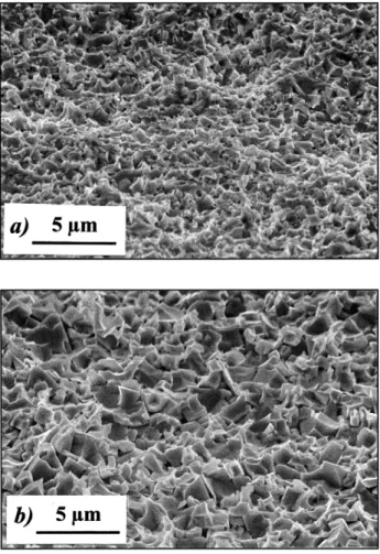
Fig. 8. Coating morphologies of 23 mm-(sample 1M10_A16, panel
a) and 11 mm-thick (sample 1M10_A8, panel b) diamond films.
Fig. 9. Raman spectra of diamond films deposited onto WC–Co inserts using process conditions A (1.5 mmyh, 1.5% CH , filament4 Ts2300 8C) and B (0.55 mmyh, 0.5% CH , filament Ts2180 8C).4
Fig. 10. Flank wear values of all tested inserts after 10 and 15 min high speed dry turning of Al–10%Al O MMC.2 3
3.2. Diamond coating characterization
Fig. 8 shows the SEM micrographs of diamond films deposited for 8 and 16 h on WC–Co inserts submitted to the two-step chemical etching (samples 1M10_A8 and 1M10_A16). Thicker films deposited for longer times using 1.5% CH4 (Fig. 8a) showed a similar morphology to those obtained with 0.5% CH . Further-4 more, they showed larger diamond grains with respect to the film deposited for 8 h using 1.5% CH4 (sample 1M10_A8, Fig. 8b). Moreover, the surface morphology of the diamond films was independent of the substrate pretreatment and WC grain size, thus indicating that film microstructure was mainly controlled by the thick-ness of the diamond coating. However, as it will be discussed later, tool life, strictly linked to the diamond adhesion level, depends on a proper combination of substrate surface morphology, produced by the different pretreatments, and WC grain size.
Fig. 9 shows the Raman spectra of the diamond coatings deposited using either A or B process condi-tions. The first-order Raman diamond peak was present
at 1338 cmy1. The frequency of this peak was 5.6ycm blue shifted with respect to natural diamond (1332.4 cmy1at atmospheric pressure and 25 8C) thus indicating a 2.2 GPa residual compressive stress in the deposited diamond w14,15x. The quality of diamond deposited using either 1.5% CH or 0.5% CH was very good, as4 4 confirmed by the low intensity of the broad band centered at approximately 1550 cmy1, attributable to sp -carbon. However, the quality of the diamond depos-2 ited using B CVD process parameters (0.5% CH and4 lower filament temperature) was slightly higher.
3.3. Turning tests
All flank wear values, measured after 10 and 15 min of dry turning Al–10%Al O MMC, are reported in Fig.2 3 10. It is worth noting that the tool coated with a less thick film(11 mm, 1M10_A8 sample) showed a severe flank wear after 10 min machining, approaching 0.5
Fig. 11. Flank wear of 1M10_A8 (panel a), 1M10_A16 (panel b),
and PCD triangular inserts (panel c) after 10 min high speed dry
turning of Al–10%Al O MMC.2 3
mm. In contrast, 1M10_A16 insert, whose 23 mm thick diamond coating was deposited on a similarly pretreated fine-grained surface, showed a much lower wear, com-parable to PCD_1 and PCD_2 tools. These data clearly put into evidence the crucial role of coating thickness in determining the tool life under specific machining conditions.
Fig. 11 shows the flank wear of the above mentioned inserts after 10 min machining. Although the measured flank wear of 1M10_A16 and PCD tools was compara-ble, the PCD flank exhibited a much more regular wear profile(Fig. 11c).
Sample 1M10_B40 showed, after both 10 and 15 min turning, flank wear values slightly smaller than those shown by both 1M10_A16 and PCD (Fig. 10). This fact might be ascribed to the higher quality of the diamond deposited using a slower growth rate. In fact, the slightly smaller amount of sp -carbon evidenced by2 Raman spectroscopy (Fig. 9) could be responsible for the observed better wear resistance.
Diamond coated 3 mm grained inserts exhibited, on average, a poorer performance with respect to chemi-cally pretreated fine-grained (1M) inserts. However, their performance was found to depend on the substrate pretreatment and cutting time. In fact, after 10 min turning, chemically pretreated (3M) samples showed flank wear values comparable to those of fine-grained inserts coated with diamond films with same thickness, and to PCD as well. The data in Fig. 10 also point out that 1 min etching with Murakami’s reagent was suffi-cient to ensure a very good adhesion of the coating. In fact, the 3M1_A16 sample exhibited a flank wear lower than 400 mm after 15 min turning and comparable to the wear of 3M10_A16 tool, although this was etched for a longer time and it was submitted to same deposition conditions.
Diamond coated 3 mm-grained inserts, which under-went thermal pretreatments(3T) prior to CVD, showed cutting performance which were independent of the specific thermal pretreatment (T9, T18 or T36, Table 2). However, the flank wear after 10 min turning was approximately 300 mm on average, i.e. larger than those exhibited by chemically pretreated substrates (3M) whose wear after the same machining time was in the 240"20 mm range. Nevertheless, after 15 min machin-ing, the wear levels were comparable(330–350 mm) to 3M coated tools, which, in turn, exhibited a worse behaviour than both fine-grained(1M) and PCD inserts. Therefore, even if the corrugation of the Co-free surface of 3M- and 3T-substrates was larger than or comparable to that of fine-grained tools (1M), the lower cutting performance exhibited by 3 mm-sized coated inserts suggests that substrate grain size plays an important role in determining the functional properties of diamond coated WC–Co tools. In fact, substrates with finer microstructure should ensure better performance due to their larger hardness. This trend was confirmed by fine-grained inserts coated with thick diamond films, which were the sole tools showing flank wear values compa-rable to PCD after 15 min dry turning.
4. Conclusions
The results showed that the performance of diamond coated WC–Co tools in dry machining highly abrasive materials such as MMCs depends on a proper combi-nation of substrate microstructure, surface pretreatment,
CVD process parameters and thickness of the deposited film.
Specifically, it was found that the finer the WC grain size, the longer the tool life of coated inserts, which were chemically etched. Both 1 and 10 min etching times with Murakami’s reagent were sufficient to achieve a proper substrate surface corrugation and a consequent good adhesion level.
Regarding the thermal treatment, satisfactory tool life was obtained with 3 mm-grained WC–Co substrates only. This kind of pretreatment would allow to reduce the use of hazardous chemicals and to consequently reduce environmental issues insofar as large scale pro-ductions of WC–Co coated parts are concerned.
Acknowledgments
The Authors are grateful to Dr Franco Arezzo for his scientific contribution and to Mr Severini and Mr Gas-perini for their technical support. Dr Polini wishes to thank Dr Giorgio Mattei (CNR-IMIP) for his valuable collaboration in collecting Raman spectra and Dr Gian-carlo Marcheselli (F.I.L.M.S. SpA) for continuous support.
References
w1x J.V. Foltz, C.M. Blackmon, Metal–matrix composites, Metals
Handbook, vol. 2, tenth ed., ASM International, 1990.
w2x S. Durante, G. Rutelli, F. Rabezzana, Surf. Coat. Technol. 94–
95(1997) 632–640.
w3x J. Gabler, L. Schafer, H. Westermann, Diamond Relat. Mater.¨ ¨ 9(2000) 921–924.
w4x M. Dai, K. Zhou, Z. Yuan, Q. Ding, Z. Fu, Diamond Relat.
Mater. 9(2000) 1753–1757.
w5x Z.M. Zhang, H.S. Shen, F.H. Sun, X.C. He, Y.Z. Wan, Diamond
Relat. Mater. 10(2001) 33–38.
w6x A. Kopf, M. Sommer, R. Haubner, B. Lux, Diamond Relat.¨ Mater. 10(2001) 790–796.
w7x R. Haubner, A. Lindlbauer, B. Lux, Diamond Relat. Mater. 2 (1993) 1505–1515.
w8x M. Nesladek, K. Vandierendonck, C. Quaeyhaegens, M. Ker-´ khofs, L.M. Stals, Thin Solid Films 270(1995) 184–188. w9x A. Inspektor, E.J. Oles, C.E. Bauer, Int. J. Refract. Met. Hard
Mater. 15(1997) 49–56.
w10x M.A. Taher, W.F. Schmidt, A.P. Malshe, E.J. Oles, A. Inspektor,
in: K.L. Mittal(Ed.), Adhesion Aspects of Thin Films, vol. 1,
VSP, The Netherlands, 2001, pp. 79–139.
w11x R. Polini, F. Bravi, F. Casadei, P. D’Antonio, E. Traversa,
Diamond Relat. Mater. 11(2002) 726–730.
w12x M. Santarelli, Thesis, University of Rome ‘Tor Vergata’, 1998. w13x R. Polini, M. Santarelli, E. Traversa, J. Electrochem. Soc. 146
(1999) 4490–4498.
w14x S.K. Sharma, H.K. Mao, P.M. Bell, J.A. Xu, J. Raman
Spectrosc. 16(1985) 350–352.
w15x A. Tardieu, F. Cansell, J.P. Petitet, J. Appl. Phys. 68(1990)