Journal of Optics
ROADMAP
Roadmap on metasurfaces
To cite this article: Oscar Quevedo-Teruel et al 2019 J. Opt. 21 073002
Roadmap
Roadmap on metasurfaces
Oscar Quevedo-Teruel
1,20,21, Hongsheng Chen
2,20,
Ana Díaz-Rubio
3,20, Gurkan Gok
4, Anthony Grbic
5, Gabriele Minatti
6,
Enrica Martini
6, Stefano Maci
6, George V Eleftheriades
7, Michael Chen
7,
Nikolay I Zheludev
8,9, Nikitas Papasimakis
8,9, Sajid Choudhury
10,
Zhaxylyk A Kudyshev
10, Soham Saha
10, Harsha Reddy
10,
Alexandra Boltasseva
10, Vladimir M Shalaev
10, Alexander V Kildishev
10,
Daniel Sievenpiper
11, Christophe Caloz
12, Andrea Alù
13, Qiong He
14,
Lei Zhou
14, Guido Valerio
15, Eva Rajo-Iglesias
16, Zvonimir Sipus
17,
Francisco Mesa
18, Raul Rodríguez-Berral
18, Francisco Medina
18,
Victor Asadchy
3, Sergei Tretyakov
3and Christophe Craeye
191
KTH Royal Institute of Technology, Stockholm, Sweden 2
Zhejiang University, People’s Republic of China 3
Department of Electronics and Nanoengineering, Aalto University, PO 15500, FI-00076, Aalto, Finland 4
United Technologies Research Center, East Hartford, CT, United States of America 5
Department of Electrical Engineering and Computer Science, University of Michigan, Ann Arbor, MI, United States of America
6Dipartimento di Ingegneria dell’Informazione e Scienze Matematiche, University of Siena, 53100 Siena, Italy
7Department of Electrical and Computer Engineering, University of Toronto, Canada 8
University of Southampton, Southampton, United Kingdom 9
Nanyang Technological University, Singapore 10
School of Electrical & Computer Engineering and Birck Nanotechnology Center, Purdue University, West Lafayette, IN 47907, United States of America
11
University of California, San Diego, CA, United States of America 12
Polytechnique Montréal, Canada
13Photonics Initiative, Advanced Science Research Center, City University of New York, New York, United States of America
14
State Key Laboratory of Surface Physics and Physics Department, Fudan University, Shanghai 200433, People’s Republic of China
15
Laboratoire d’Electronique et Electromagnétisme, Sorbonne Université Paris, Paris, France 16
University Carlos III of Madrid, Madrid, Spain 17
Faculty of Electrical Engineering and Computing, University of Zagreb, Zagreb, Croatia 18
University of Seville, Seville, Spain 19
Université Catholique de Louvain, Belgium
E-mail:[email protected],[email protected]@aalto.fi Received 12 October 2018, revised 19 December 2018
Accepted for publication 4 April 2019 Published 1 July 2019
Abstract
Metasurfaces are thin two-dimensional metamaterial layers that allow or inhibit the propagation of electromagnetic waves in desired directions. For example, metasurfaces have been
demonstrated to produce unusual scattering properties of incident plane waves or to guide and modulate surface waves to obtain desired radiation properties. These properties have been employed, for example, to create innovative wireless receivers and transmitters. In addition,
J. Opt. 21(2019) 073002 (44pp) https://doi.org/10.1088/2040-8986/ab161d
20 Guest Editors of the Roadmap. 21
metasurfaces have recently been proposed to confine electromagnetic waves, thereby avoiding undesired leakage of energy and increasing the overall efficiency of electromagnetic instruments and devices. The main advantages of metasurfaces with respect to the existing conventional technology include their low cost, low level of absorption in comparison with bulky
metamaterials, and easy integration due to their thin profile. Due to these advantages, they are promising candidates for real-world solutions to overcome the challenges posed by the next generation of transmitters and receivers of future high-rate communication systems that require highly precise and efficient antennas, sensors, active components, filters, and integrated technologies. This Roadmap is aimed at binding together the experiences of prominent researchers in thefield of metasurfaces, from which explanations for the physics behind the extraordinary properties of these structures shall be provided from viewpoints of diverse theoretical backgrounds. Other goals of this endeavour are to underline the advantages and limitations of metasurfaces, as well as to lay out guidelines for their use in present and future electromagnetic devices.
This Roadmap is divided intofive sections:
1. Metasurface based antennas. In the last few years, metasurfaces have shown possibilities for advanced manipulations of electromagnetic waves, opening new frontiers in the design of antennas. In this section, the authors explain how metasurfaces can be employed to tailor the radiation properties of antennas, their remarkable advantages in comparison with conventional antennas, and the future challenges to be solved.
2. Optical metasurfaces. Although many of the present demonstrators operate in the microwave regime, due either to the reduced cost of manufacturing and testing or to satisfy the interest of the communications or aerospace industries, part of the potential use of metasurfaces is found in the optical regime. In this section, the authors summarize the classical applications and explain new possibilities for optical metasurfaces, such as the generation of superoscillatoryfields and energy harvesters.
3. Reconfigurable and active metasurfaces. Dynamic metasurfaces are promising new platforms for 5G communications, remote sensing and radar applications. By the insertion of active elements, metasurfaces can break the fundamental limitations of passive and static systems. In this section, we have contributions that describe the challenges and potential uses of active components in metasurfaces, including new studies on non-Foster, parity-time symmetric, and non-reciprocal metasurfaces.
4. Metasurfaces with higher symmetries. Recent studies have demonstrated that the properties of metasurfaces are influenced by the symmetries of their constituent elements. Therefore, by controlling the properties of these constitutive elements and their arrangement, one can control the way in which the waves interact with the metasurface. In this section, the authors analyze the possibilities of combining more than one layer of metasurface, creating a higher symmetry, increasing the operational bandwidth of flat lenses, or producing cost-effective electromagnetic bandgaps.
5. Numerical and analytical modelling of metasurfaces. In most occasions, metasurfaces are electrically large objects, which cannot be simulated with conventional software. Modelling tools that allow the engineering of the metasurface properties to get the desired response are essential in the design of practical electromagnetic devices. This section includes the recent advances and future challenges in three groups of techniques that are broadly used to analyze and synthesize metasurfaces: circuit models, analytical solutions and computational methods.
Keywords: metasurfaces, two-dimensional metamaterials, antennas, high-rate communications (Some figures may appear in colour only in the online journal)
Contents
METASURFACE BASED ANTENNAS 4
2. Modulated metasurface antennas 6
3. Huygens’ metasurfaces for selected antenna applications 9
OPTICAL METASURFACES 11
4. Metasurfaces beyond quasi-holography: creating unusual electromagneticfield structures in free-space 11
5. Refractory plasmonic metasurfaces 13
RECONFIGURABLE AND ACTIVE METASURFACES 16
6. Current and future directions in tunable and active metasurfaces 16
7. Nonreciprocal metasurfaces 19
8. Active and reconfigurable metasurfaces 21
9. Tunable metasurfaces 23
METASURFACES WITH HIGHER SYMMETRIES 26
10. Dispersive properties of periodic surfaces with higher symmetries 26
11. Application of glide-symmetric periodic holey structures to gap waveguide technology 29
12. Quasi-analytical methods for periodic structures with higher symmetry 31
NUMERICAL AND ANALYTICAL MODELLING OF METASURFACES 33
13. Analysis of metasurfaces via an equivalent circuit approach 33
14. New perspectives on the modeling of metasurfaces 35
METASURFACE BASED ANTENNAS
1. Tailoring aperturefields with metasurfaces Gurkan Gok1and Anthony Grbic2
1United Technologies Research Center, East Hartford, CT,
United States of America
2Department of Electrical Engineering and Computer Science,
University of Michigan, Ann Arbor, MI, United States of America
Status. Tailoring aperture fields in phase, amplitude and polarization is the key aim of versatile antenna systems. An aperture’s amplitude and phase characteristics govern the beam shape, beam pointing direction, and beam polarization. Traditionally, aperture fields of high gain microwave and millimeter-wave antennas have been established by reflectors/lenses excited by simple feed antennas (e.g. dish antennas, lens antennas, reflectarrays, transmitarrays), and steered by mechanical means. This conventional approach results in large and heavy structures, due the bulky reflectors/ lenses, gimbals and displaced feed antennas employed. Alternatively, apertures can be composed of discrete antenna elements, and electronically controlled, as in the case of phased arrays. Phased arrays, however, are costly and exhibit high feed network losses that grow with aperture size and frequency.
Recent developments in metasurfaces have opened new opportunities in antenna design. Metasurfaces are surfaces textured at a subwavelength scale to achieve tailored electromagnetic surface properties. They hold promise for the development of low cost, light weight, and compact antennas capable of producing arbitrary aperture fields. Metasurfaces transform wavefronts by impartingfield discontinuities across their thin and potentially electrically large and/or conformal surfaces. Their ability to control wavefronts through texture allows for the separation of geometry from electromagnetic functionality. Thus, metasurfaces can take on various form factors, while controlling waves through their subwavelength pattern/granularity. This is in contrast to traditional lenses, which control waves through geometry/shape.
Metasurface antennas can transform fields of a source excitation into an arbitrary radiating aperturefield, either by judiciously guiding waves toward an aperture that radiates, or by supporting leaky-waves that directly radiate targeted radiation patterns. In[1], anisotropy and inhomogeneity were
exploited to transform a sourcefield into a complex (phase and amplitude) aperture through the manipulation of the phase and powerflow of guided waves, allowing independent control of an aperture’s phase and amplitude distributions. Various one-dimensional aperture profiles, in phase and amplitude, were theoretically demonstrated[1]. The approach
was used to demonstrate beamformer antennas implemented using transmission-line based metamaterials possessing anisotropic material properties and a true-time-delay response [2]. The beamformers achieved beam scanning through a
lateral displacement of its feed. The approach was later extended to design aperture antennas that can excite tailored (aberration free) beams for displaced feed locations [3] (see
figure1(a)). Simulated radiation efficiencies over 30% were
reported between 10 GHz and 13 GHz for beam scanning between ±30°, in 10° steps. Beam pointing directions remained constant over the operational band due to the true-time-delay behavior of the design. Coupling between feedlines degraded antenna patterns below 10 GHz. Analo-gously, cascaded metasurfaces have been recently reported that can create complex aperture fields with arbitrary phase and amplitude profiles through sequential, lossless and reciprocal phase manipulation[4].
There has also been significant activity in the develop-ment of traveling-wave metasurface antennas[5]. In addition,
metasurface-based lenses that are directly integrated with feed antennas have been reported [6]. Such lens-based antennas
have demonstrated an order of magnitude reduction in thickness compared to traditional lens-based antennas [7]
(see figure 1(b)). An experimental lens-antenna system
operating at 9.9 GHz with approximate radiation efficiency of 50%, aperture efficiency of 70%, half-power gain bandwidth around 8%, and impedance bandwidth of around 4% was reported [7]. The low-profile metasurface lens
antenna was designed by cascading two functional metasur-faces over a radial cavity. The first metasurface supports a cylindrical leaky-wave which illuminates the second metasur-face. The second metasurface, phase and polarization correct Figure 1.Metasurface antennas can transformfields of a source excitation into arbitrary radiating aperturefields either by (a) guiding them towards an aperture that radiates[3], or (b) supporting traveling/leaky-waves that radiate directive radiation patterns [7]. (a) © 2018 IEEE. Reprinted, with permission, from [3]. (b) © 2015 IEEE. Reprinted, with permission from[7].
the emitted radiation, creating directive radiation patterns of linear or circular polarization. The two metasurfaces essen-tially form an asymmetric (bianisotropic) metasurface that allows one to tailor the reflected and transmitted phase, as well as transmission/reflection amplitude. Such an approach demonstrated a path towards modular antenna design, where layers of metasurfaces are cascaded to tailor the aperture of directly-fed, low-profile antennas. The approach eliminates the displaced feed typically used in lens and reflector antennas. Single metasurfaces above a thin cavity have also been reported that tailor cavity modes into arbitrary aperture fields [8, 9]. These extremely low-profile, high gain
antennas that employ a single metasurface with bianiso-tropic properties have demonstrated precise control of radiation patterns.
Current and future challenges. Although metasurface-based antennas show great promise for dramatically reducing the size and complexity of antenna systems, certain challenges lie ahead for their mass deployment. Metasurfaces consist of subwavelength resonators with electromagnetic properties that are often times frequency dispersive. In other words, the resonant nature of a metasurface’s constitutive elements can restrict the usable bandwidth of metasurface-based antennas. Single layer metasurface antennas with operational bandwidths of up to 8% have been reported [7, 8, 10]. In
comparison, a commercially available Ku-band SATCOM antenna covers global receive and transmit bands nearing a total bandwidth of 23%. Furthermore, if simultaneous operation in multiple satellite communication bands is desired with a single antenna, even larger bandwidths or multiband performance[11] are needed.
Electrically addressable/reconfigurable metasurfaces pose further challenges. High gain antennas with dynamic beam steering are often needed/desired in wireless applica-tions ranging from satellite, 5G communicaapplica-tions to remote sensing, imaging and radar. The introduction of tunability can limit performance (increase loss, limit bandwidth, etc) and result in complex control (tuning, biasing, etc) circuitry. Mechanisms such as externally controllable circuit compo-nents(varactors, pin diodes) [12] and liquid crystal layers [13]
have been investigated for dynamic reconfigurability. Circuit-based approaches face scaling challenges in high gain metasurfaces. With increased size, the number of components dramatically increases, along with cost and losses, if deep subwavelength cell dimensions are maintained. Liquid crystal layers are scalable, and have shown promising results at mm-waves. However, they are relatively slow with millisecond response times. As for the complexity of the control circuitry, questions remain on how such circuitry can be incorporated without interfering with the microwave/millimeter wave performance of the metasurface.
Metasurfaces have provided antenna designers with an enhanced surface parameter set, but how does one exploit these added degrees of freedom to design a metasurface antenna with a specified aperture distribution? Transformation
optics provides a systematic approach to tailoring radiating apertures[14,15]. However, the approach has been limited to
tailoringfields from a single elementary source.
Advances in science and technology to meet challenges. Improvements to the bandwidth of metasurface-based antennas can be made by combining the spatial field manipulation offered by metasurfaces with traditional filter concepts, in order to provide both spatial and spectral manipulation of fields. Maximally linear phase responses and true-time-delay responses have been achieved usingfilter concepts in lens-based antennas and reflectarrays [16, 17].
These approaches have shown to be effective at microwave frequencies. However, the multilayer fabrication needed to realize these metasurfaces becomes increasingly challenging at higher frequencies. It should also be noted that the broad bandwidths observed with transmissive or reflective metasurfaces have not translated to broadband, directly-fed metasurface-based antennas.
Advanced design techniques that integrate control circuitry into metasurface design, as well as the development of synthesis approaches for multi-input multi-output designs, can tackle some of the challenges associated with recon figur-able metasurfaces. Spatial light modulators use transparent conductors and thin film transistors to realize electrically addressable pixels/cells, but such transparent control circuitry is not available at microwave and millimeter-wave frequen-cies. Therefore, metasurface patterns at these frequencies must serve a dual purpose: provide the microwave/mm-wave surface properties needed, as well as incorporate the control/ bias circuitry[18].
A synthesis technique for multi-input, multi-output metasurface devices (i.e. devices that are capable of transforming distinct source field distributions to distinct tailored beams) through compound metasurfaces (multiple cascaded metasurfaces) would allow a number of function-alities to be incorporated into a single device. Such an approach could remove the need for a reconfigurable mechanism for a finite number of functionalities. Towards this goal, a transformation medium that maps different excitations to specified output beams was recently designed through optimization, and reported in[4].
Concluding remarks. Metasurfaces provide new opportunities for the development of compact, low-cost and versatile antennas and quasi-optical systems. Although promising, performance and synthesis challenges, as well as tuning/reconfiguration mechanisms must be addressed before their use in antenna design becomes widespread. Metasurface antennas/radiators that are low-profile, low cost, fabricable over large areas, and offer extended capabilities could see wide scale deployment in various application areas ranging from terrestrial/satellite communication systems and aerial platforms, to radar and surveillance systems.
2. Modulated metasurface antennas Gabriele Minatti, Enrica Martini and Stefano Maci
Dipartimento di Ingegneria dell’Informazione e Scienze Matematiche, University of Siena, Via Roma, 56 53100 Siena, Italy
Status. Modulated metasurface (MTS) antennas have emerged in the last ten years as a new concept of aperture antennas radiating by leaky-wave (LW) effect. The LW originates from a cylindrical wavefront surface-wave (SW) excited by a monopole and propagating on an MTS which imposes suitably modulated impedance boundary conditions (IBCs). Energy is leaked when the SW wavelength is properly matched to the local period of the periodic or quasi-periodic IBCs provided by the MTS. Through the MTS, amplitude, phase and polarization of the radiativefield can be controlled to obtain desired radiation performance.
An MTS antenna is composed of a host medium with many small metallic or dielectric inclusions, often referred to as‘pixels’, arranged in a regular lattice (figure2). Due to the
smaller losses, all-metallic technology is preferred to the printed dielectric technology at higher frequencies(above Ka-band). The SW is provided by a feeding system embedded in the MTS itself, which can be as simple as an elementary transverse magnetic(TM) radiator. The basic configuration of an MTS antenna therefore has a simple low profile structure. Amongst many, the most intriguing feature of MTS antennas is that performance can be easily tailored to a wide variety of application requirements, without significantly changing the fundamental structure. A simple modification of the global holography of the MTS leads to beam tilting, beam shaping, and polarization control. An example is shown in figure 3. This feature indeed opens the path to the research on dynamically adaptive MTS antennas which are able to steer or reconfigure the beam. The main concept is to dynamically change the IBCs offered by the MTS by acting on the inclusions composing the MTS through active devices or tunable materials.
Structures based on PCB layout are presently the most mature configuration for MTS antennas: the feasibility of the concept is well documented in literature (see, for instance, [19–22]) proving that the beam can be controlled in its
shape, direction and polarization. A significant effort has been dedicated in recent years to develop effective design procedures, which now have reached a significant level of maturity[23]. The structural characteristics of these antennas
are extremely appealing: MTS antennas are cost effective, easily manufactured with standard PCB techniques or 3D printing devices. They are light, low encumbrance and in principle conformable to different kinds of surfaces. These are intriguing features both for commercial and space applica-tions(for which they were originally conceived [24]).
Figure 2.Metasurface antenna layout. An SW excited from the centre is gradually converted into a radiative LW by interacting with the MTS. At microwaves, the MTS is usually formed by a texture of printed patches on a grounded dielectric slab(right inset).
Alternatively, usually at millimetre waves, the MTS can be formed by a tight distribution of metallic pins(left inset).
Figure 3.Dynamically adaptive MTS. By simply changing the IBCs offered by the MTS, the beam can be easily redirected without affecting the antenna structure.
Despite the MTS antenna concept being introduced a few years ago, there are still open issues. The most notable one is pattern bandwidth [25], i.e. pattern stability with respect to
frequency, which is still a subject of concern. Pattern bandwidth is mainly limited by the mismatch between the SW wavelength and the periodicity of the IBCs occurring when the operational frequency changes from the design one. Instead, matching bandwidth, i.e. return loss bandwidth, is a minor limitation for the overall antenna bandwidth. Indeed, MTS antennas can be easily matched and, given the small size of the pixels, the MTS is far from resonance[24]. However,
the performance in terms of the bandwidths of these antennas is quite robust with respect to alternative printed dipole technologies (i.e. patch array) with a simple feed point. Indeed, for constant average impedance MTS, with possibly non-uniform modulation index and uniform modulation period, the bandwidth is approximated by the simple formula
B v c a B v c a 0.95 g 1; 1.2 g 1 1 » » l l ⎛ ⎝ ⎜ ⎞⎠⎟ ( )
where vg is the group velocity of an SW propagating on the average impedance of the MTS, c is the speed of light in free space and alis the radius in free-space wavelengths. Thefirst equation in(1) is relevant to a uniform modulation of the IBC,
while the equation in brackets is relevant to an optimized IBC modulation [25]. The corresponding expressions of the
product bandwidth-gain are
BG v ca BG v c a a a 22 ; 47 2 . 2 g g » » + l l l l ⎛ ⎝ ⎜ ⎡ ⎣⎢ ⎤ ⎦⎥ ⎞ ⎠ ⎟ ( ) ( )
The above equations also establish physical limits in the product bandwidth-gain as22al(47al) Better performance in. terms of radiation-pattern bandwidth can be obtained by a non-uniform modulation period, namely by matching the local radial period of the modulation at different positions with the SW wavenumber at different frequencies. This leads to space-variable shapes of the holography conceptually similar to those obtained in spiral active region antennas. With this, one can enlarge the bandwidth to a wideband operation (till 25%), at the price of a significantly lower aperture efficiency. The performances of the bandwidths expressed in equations(1) and (2) are, however, suitable for
many applications, including those for space, considering the fact that MTS antennas with more than 41 dBi of directivity have been recently measured in Ka-band.
Current and future challenges. Fast reconfigurability of the beam, beam scanning and multibeams are the most applicative impactful challenges today. Low-cost beam scanning antennas are particularly appealing for Sat-Com on the move and adapt well to the potential performance of the MTS technology. Fast beam hopping and multibeam operations with low power consumptions are interesting features for 5G applications. Overlapping apertures for
multi-beaming are in fact already successfully devised for MTS antennas in static configuration, and exhibit promising potential on this concern. The possibility to easily customize the antenna feature in nearfield focusing also opens the door towards medical applications.
Dynamic, electronically reconfigurable MTS antennas need to be improved in terms of efficiency. The concept has already been demonstrated [26–28], where the inclusions of
the MTS are loaded with active devices or they include liquid crystals or phase changing materials like vanadium dioxide. The electric features of the inclusions become voltage controlled and hence the IBCs offered by the MTS can be properly adjusted by an external control. Active devices or phase changing materials yield an increase of the antenna losses with a consequent reduction of gain and increase of power demand; losses become more important when working at higher frequencies(e.g. Ka-band): frequency scalability is indeed another future challenge. Also, phase changing materials suffer from temperature instability[29]. Alternative
strategies make use of optical pumping of silicon or gallium arsenide substrates to alter the electrical properties of the inclusions. Losses become less critical when dealing with a mechanical reconfiguration. The use of micromechanical systems or piezoelectric devices have been proposed[30], but
they may suffer from low reliability and an MTS antenna based on such devices may be too sensitive to the external vibrations if installed on moving vehicles.
Advances in science and technology to meet challenges. Despite the significant advances done in the framework of the design procedure [23], antenna optimization is still a future
challenge topic. Whenever strong requirements on performance are demanded, it is necessary to optimize the final MTS layout which may be composed by up to a hundred thousand elements. Managing the high number of inclusions with numerical methods requires smart strategies which make combined use of homogenized boundary conditions and fast integral-equation solvers.
Extension of the MTS antenna concept to curved surfaces is a future challenge for conformable and aerodynamic applications. Meeting this challenge implies an extension of the creeping-wave theory to metasurface coated curved surfaces, which are almost absent at the present state of the art and would require a significant effort.
Advances in phase changing materials would bring a significant benefit to MTS antennas, in terms of losses and switching time reduction, as well as increase of temperature stability. Special liquid crystals for microwaves could be extremely beneficial, and some companies are investing in this direction. MTS with integrated active devices, instead of discrete active devices, would also bring advantages in terms of reliability, losses and performance. Realizing integrated devices on a wide area will require significant improvement of the accuracy and repeatability of the fabrication processes. 3D printing processes are also extremely appealing for MTS antennas, creating the possibility to move beyond the classical PCB processes, offering chances to build up the MTS, adding
specific features to the inclusions and hence improving performance with low-cost.
Concluding remarks. The operation principle of MTS antennas allows for tailoring the MTS with active devices, liquid crystals or phase changing materials in real time. While the initial concern of some time ago about bandwidth is a
challenge in fast progress, losses, agility and dynamic speed are still open issues for both design and fabrication technology aspects. We have presented here challenges and perspectives of MTS antennas in the microwave domain. However, the operational principle behind SW control
through MTS can be applied to a wide range of
3. Huygens’ metasurfaces for selected antenna applications
George V Eleftheriades and Michael Chen
Department of Electrical and Computer Engineering, Uni-versity of Toronto, Canada
Status. Electromagnetic surfaces for antenna applications have a long history and include frequency-selective surfaces, transmit and reflect arrays, and more recently tensorial holographic surfaces[31]. Recently, metasurfaces have been
introduced as 2D analogues of metamaterials [32]. Their
unique characteristic is that these metasurfaces feature sub-wavelength unit cells, such that they can be homogenized with electric and magnetic surface susceptibilities or equivalent impedances and admittances. In this contribution, we will describe some recent advances of such metasurfaces for antenna applications.
Huygens’ or ‘field-discontinuity’ metasurfaces when illu-minated by an incident electromagnetic wave induce electric and magnetic dipole moments, which correspond to electric and magnetic surface current densities; see equation (3) [33, 34].
These currents, when properly excited, can shape the transmitted or reflected electromagnetic wave at will (see figure4(a)).
Js=n´ H2 -H1 ,Ms= - ´n E2 -E1 . 3
+ - +
-ˆ ( ) ˆ ( ) ( )
The challenge here is how to synthesize these surfaces so that the incidentfield can excite the required currents (3) to perform a
desiredfield transformation. This can be aided by casting the problem in terms of spatially varying impedance and admittance sheets; see equations(4).
Et avg, =Zse·Js-Kem· [ ˆn´Ms] (4a) Ht avg, =Ysm·Ms-Kem· [ ˆn´Js]. (4b)
A natural embodiment of such Huygens’ surfaces consists of an array of loaded strips and loops which can be tuned to synthesize the required surface reactances(4) (see figure4(b)). In this way,
such surfaces are conducive to antenna pattern shaping when illuminated by plane waves or by the fields from nearby elementary feeding sources.
To demonstrate the capability of these Huygens’ metasurfaces (HMS), figures 4(c) and (d) show the case of
reflectionless refraction of a normally incident plane wave at an extreme angle[35,36]. This becomes possible because, on
the one hand, the surface can excite both electric and magnetic dipole moments (3). On the other hand, these
electric and magnetic dipole moments can be coupled together to provide a bi-anisotropic response as represented by the term Kemin(4) [37]. In this way, the angle-dependent
impedance of the transmitted wave can be perfectly matched to the different impedance of the incident wave, with a passive and lossless surface.
A natural antenna application of these metasurfaces is for gain enhancement. A typical scenario is that of placing a low-directivity feeding antenna at the focal plane of a metasurface lens. In figure 5(a), we show the case of a cylindrical lens
Figure 4.(a) The concept of a Huygens’ metasurface [38]. (b) A loaded strip-loop unit cell[40]. (c) A reflectionless refracting bi-anisotropic metasurface tested using a quasi-optical system at 20 GHz[36]. (d) Full-wave simulation of reflectionless refraction for normal incidence to 71.8 degrees.(a) [38] 2018 Nature Commu-nications. With permission of Springer.CC BY 4.0.(b) © 2017 IEEE. Reprinted, with permission, from[40]. (c) Reprinted figure with permission from[36], Copyright (2018) by the American Physical Society.
Figure 5.(a) A collimating Huygens’ metasurface lens [39]. (Inset) A‘spider’ unit cell has been used. (b) Beam collimation in the E-plane at 35.2 GHz[39]. (Inset) Top view of the metasurface metallization pattern.(c) Concept of a cavity excited metasurface to synthesize arbitrary antenna patterns[38]. (d) Synthesized one-parameter Taylor’s distribution with sidelobes <−20 dB [40]. (a), (b) © 2018 IEEE. Reprinted, with permission, from [39]. (c) [38] 2018 Nature Communications. With permission of Springer.CC BY 4.0.(d) © 2017 IEEE. Reprinted, with permission, from [40].
antenna, implemented as a thin and flat Huygens’ metasur-face, to enhance the gain of a feeding slotted-waveguide antenna. For this, a‘spider’ unit cell has been used, as shown in the inset offigure5(a) [38]. The slotted waveguide exhibits
a narrow beamwidth along the length of the guide(H-plane) but a wide beam along the transverse plane (E-plane). The metasurface lens placed in close proximity to the waveguide leaves the H-plane unchanged but collimates the E-plane considerably leading to an average gain enhancement of 10 dB around 35 GHz(see figure5(b)) [39].
The advanced capability of these Huygens’ metasurfaces is highlighted in the case of arbitrary antenna pattern synthesis. The general idea is to illuminate an HMS with an elementary pattern and transform this through the surface to an arbitrary antenna pattern. A possible embodiment of this concept is to embed an elementary feed antenna in an open cavity which is closed by a suitable HMS as shown in figure 5(c) [38]. The transmitted fields can be stipulated to
correspond to a ‘virtual array’ with desired weights to synthesize a certain antenna pattern(in both magnitude and phase) [40]. The incident fields are a superposition of N
cavity modes, each one characterized by a characteristic reflection coefficient .G A bi-anisotropic HMS can be used ton
determine the reflection coefficientsG such that local powern
conservation is achieved. The latter condition is required to ensure a metasurface that is passive and lossless(in principle). The reflection coefficients G can be determined using an
suitable optimization algorithm. In this way, arbitrary antenna patterns, in terms of beamwidth and sidelobe structure, can be synthesized as shown infigure5(d).
It should be understood that the method described above is in general applicable to other scenarios and not just for cavity excited metasurfaces. For example, one could envision a feed antenna exciting a pair of bi-anisotropic HMSs [41].
The fields in the region between the metasurfaces can be expanded in terms of N plane waves with weightsG such thatn
local power conservation is enforced, for a given desired excitation of the weights on the output‘virtual array’.
Current and future challenges
The versatility of the HMS has been highlighted in the pre-vious section. In principle, these surfaces can manipulate at
will the phase, magnitude and polarization (as implied by the general tensorial nature of (4)) of an incident wave.
Despite this versatility, a challenge that remains is the dif-ficulty to translate the spatially varying Z ,se Y ,sm Kem
para-meters in(4) using physical structures such as the wire-loop
or other 3-metal-layer structures (see the inset in figure 5(a)). This can be a time-consuming process,
requir-ing many trial and error steps to build a suitable geometry/ material library for each physical platform. To address this challenge, dedicated electromagnetic CAD tools will need to be developed combined with suitable optimization routines. Another challenge that needs to be addressed directly is that of the bandwidth. To appreciate this, consider the simple example of a dielectric lens and its corresponding planar HMS implementation. The physical lens features extremely large bandwidth in terms of reflections and chromatic aberration (at least at microwave frequencies where dielec-trics like glass have very little dispersion). However, typi-cally HMSs will suffer from several effects that will limit their bandwidth. For example, at the cell level, there can be appreciable dispersion which would depart from the ideal frequency variation that is implied by (4) (typically
corresponding to a linear transmission phase). Moreover, such HMS lenses would resemble zoned dielectric lenses, which would introduce additional frequency variation due to the zoning effect. This represents an opportunity for future development of broadband and/or multiband HMS [42].
Another challenge that opens up new opportunities is to render these metasurface antennas beam-scannable or, in general, reconfigurable. For this purpose, one can envision two possible avenues. The first would be to equip each constituent unit cell with simple electrically tunable element (s), such as varactors, transistors or even liquid crystals. This would alter their local impedance and achieve desired transformations in real time based on (4). However, the
benefits and drawbacks of such an approach compared to traditional methods such as electronically scannable phased arrays should be carefully evaluated. The second avenue would be to use the metasurfaces as radomes, which are either fixed or of limited agility, above smaller phased arrays. In this way, the metasurface radome can be used to enhance the gain or the angular scan range of the underlying phased array [43].
OPTICAL METASURFACES
4. Metasurfaces beyond quasi-holography: creating unusual electromagneticfield structures in free-space
Nikolay I Zheludev and Nikitas Papasimakis
University of Southampton, Southampton, United Kingdom Nanyang Technological University, Singapore
A few words about terminology and state of the art. The history of photonic metamaterials has largely been the history of metasurfaces, or planar metamaterials. Indeed, the majority of work on three-dimensional metamaterials has taken place in the microwave domain, where the fabrication of volume multi-layered structures is easier. Planar and quasi-planar metasurfaces have helped to observe a wide range of important effects including enhanced (nearly perfect) absolute absorption, giant linear and circular dichroism, negative index of refraction, Lorentz-reciprocity-compliant asymmetric transmission, toroidal dipole excitations and many other phenomena that are difficult or impossible to study in natural media.
However, in the current literature, the term‘metasurface’ is predominantly used in relation to phenomena associated with wavefront modifications of electromagnetic radiation by diffraction on a planar metamaterial. Similarly to holography, the objective is to control thefield structure in free space by appropriate patterning of a medium (metamaterial), which scatters electromagnetic radiation. Initial efforts in this research field involved the generation of radially and azimuthally polarized beams by space-variant dielectric subwavelength gratings[44] and the observation of
polariza-tion changes of light upon diffracpolariza-tion by gammadions assembled from metallic V-shaped elements [45]. The
demonstrations of metasurface-based lenses [46] and
wave-vector selective metasurfaces, transparent only within a narrow range of light propagation directions operating as tunnel visionfilters [47], also belong to this class of effects.
The field of metasurfaces gained considerable prominence and massive follow-up after the demonstration of anomalous refraction on gradient metasurfaces[48] and the development
of high-throughput metasurfaces for focusing of light[49].
Emerging applications of metasurfaces. New, interesting and important future directions for metasurfaces will go beyond mimicking holograms, lenses or diffraction gratings, aiming at creating uniquefield structures that are not attainable with conventional optical elements. Below, we will consider two examples of such metasurfaces.
We envisage that an important direction for metasurfaces is the generation of superoscillatory fields. Indeed, a conventional lens cannot focus free-space light beyond half of the wavelength, λ. Nevertheless, precisely tailored interference of multiple waves can form a hotspot in free space of arbitrarily small size known as superoscillation.
Recently, a new type of metasurface was demonstrated that generated electromagneticfield profiles with structural features at theλ/100 scale in free space [50]. The metasurface creates a
sub-diffraction hotspot surrounded by nanoscale phase singula-rities(∼λ/50 in size) and zones where the phase of the wave changes more than tenfold faster than in a standing wave. These areas with high local wavevectors are pinned to phase vortices and zones of energy backflow (∼λ/20 in size) that contribute to subtle and relatively small tightening of the main focal spot size beyond the Abbe-Rayleigh limit. Such superoscillatory free space fields offer new opportunities for nanoscale metrology and imaging.
Another direction of research where metasurfaces can be indispensable is the generation of non-separable space-time electromagnetic excitations that exist only in the form of short bursts of energy propagating in free space at the speed of light. Typical examples of such excitations are the ‘flying doughnuts’ [51], which are distinguished from transverse
waves by a doughnut-like configuration of electric and magnetic fields with strong longitudinal field components along the propagation direction.
The generation of flying doughnut pulses presents a number of substantial challenges associated to their unusual spatiotemporal structure. For example, the few-cycle nature of the pulse requires a broadband source, while the frequency Figure 6.Sketch of metamaterial converter for the generation of flying doughnut pulses. The metasurface consists of azimuthally oriented dipole resonators arranged in concentric rings. The inset at the bottom left of thefigure shows a false colour image of a flying doughnut pulse, experimentally generated by a plasmonic metasur-face(fabricated by focused-ion-beam milling) [53]. The high frequency components close to the centre of the pulse are indicated by the blue-green colour, while the red colour in the periphery of the pulse corresponds to the lower frequency components, in accordance with the space-time non-separable nature of the pulse.
content of the pulse varies substantially along the radial direction. Such flying doughnuts can be generated from conventional pulses using a singular metamaterial converter designed to manipulate both the spatial and spectral structure of an input pulse[52,53]. The metamaterial converter can be
constructed by a cylindrically symmetric array of low Q-factor dipole resonators oriented radially or azimuthally oriented electric dipoles and arranged in concentric rings(see figure6). The spatiotemporal coupling is provided by varying
the resonant properties of the metamaterial elements across the radial direction. The ability to generateflying doughnuts is of fundamental interest, and as such pulses shall interact with matter in unique ways, including nontrivial field transformations upon reflection from interfaces and the
excitation of toroidal response and anapole modes in matter, hence offering opportunities for telecommunications, sensing, and spectroscopy.
Acknowledgments
This work was supported by the Singapore Ministry of Education (Tier 3 Grant MOE2016), the Engineering and Physical Sciences Research Council UK (Grant EP/ M009122/1), and the European Research Council (ERC) under the European Union’s Horizon 2020 research and innovation programme(Grant Agreement No. 786851).
5. Refractory plasmonic metasurfaces
Sajid Choudhury, Zhaxylyk A Kudyshev, Soham Saha, Harsha Reddy, Alexandra Boltasseva, Vladimir M Shalaev and Alexander V Kildishev
School of Electrical & Computer Engineering and Birck Nanotechnology Center, Purdue University, West Lafayette, IN 47907, United States of America
Status. Optical metasurfaces (MSs) emerged with the promise of manipulating light at a sub-wavelength scale. The concept of MSs has been utilized to create ultra-compact and subwavelengthflat optical elements—lenses, holograms, color filters, waveplates, etc. (For more detailed reviews on MS applications, please refer to [54–66]). However,
plasmonic and dielectric MSs have been broadly used primarily for room temperature applications. The inherently small footprint for MS components requires a tradeoff between the high field confinement and lower damage threshold. In dielectric MSs, the losses are lower and thus this class of MSs could be used to make high-temperature devices. However, thefield confinement in a dielectric MS is much smaller than in its plasmonic counterparts. Additionally, losses are beneficial in applications where the power absorbed through loss is harvested as heat.
Thermal to photovoltaic energy conversion can be obtained by selectively converting heat energy to emitted radiation at a wavelength. The radiation is then absorbed by a photovoltaic (PV) cell that converts it to an electromotive force to drive external current through a circuit. A solar absorber can be combined with the emitter to convert solar energy first to heat and then to the selective radiation band corresponding to the PV cell. Recently, it has been theoretically predicted that by judiciously tailoring the spectral properties of the emitters and absorbers components using metasurfaces, the efficiency for direct energy conver-sion from solar/thermal energy to electricity could potentially reach an unprecedented value of∼85% [67]. This estimated
theoretical efficiency is in striking contrast to the current physical limitation (∼30%) imposed by the Shockley-Queisser limit [68] for a single silicon p-n junction cell
[69]. The development of optical MS structures would open
new frontiers for realization of solar thermophotovoltaic and thermophotovoltaic systems. Both systems require metasur-face elements operating at a very high temperature (>1000 °C).
Thermophotovoltaics (TPV). In a TPV system, thermal radiation is directly converted to electricity via the photovoltaic (PV) effect. A TPV system consists of a PV cell array and a selective emitter with the emissivity matching absorption band of a PV cell. A schematic of a TPV system is shown infigure7(a). TPV energy conversion offers numerous
significant advantages over competing technologies [70,71].
These include the realization of highly versatile, modular, low-weight and compact electric generators (portable or stationary), which are noiseless, low-maintenance and
energy-efficient [72]. Optimal TPV energy conversion
requires large area metasurface emitters (see figure 7(a)).
Hence, robust refractory materials, which are compatible with low-cost, large-area fabrication-techniques, are critical for practical highly-efficient metasurface TPV elements.
Solar thermophotovoltaics (STPV). An STPV system comprises an absorber, an emitter, and PV cells, as shown in figure 7(b). The absorber, heated by concentrated solar
energy, increases the temperature of the emitter, which is engineered to radiate within the specific band where the absorption of a PV cell is at its maximum. Hence, by absorbing broadband solar energy and then re-emitting it within a desired working band of the PV cell array, the MS-based STPV architecture provides an efficient way of harvesting solar energy[69].
Current and future challenges. The inherent ability of MSs to tailor the absorbances/emittances of optical surfaces is of great interest in TPV and STPV. The functionality of MSs can be further enhanced by designing emitters that operate at elevated temperatures and match the spectrum of solar radiation, thus maximizing the absorption. MS resonant superabsorbers have already demonstrated polarization independent absorption in the entire visible spectrum [73].
The absorption/emission can also be engineered to match that of energies emitted by other forms of radiative emitters, such as a nuclear reactor, engine, or combustion chamber [74].
Plasmonic metasurface emitters for STPV and TPV require materials that maintain good optical properties at high-temperatures and field intensities [75]. Conventional noble
metals (Au and Ag) have low melting points and damage thresholds. Nano-structuring these materials further decreases the maximum temperature that they can withstand. At high temperatures, gold MSs were shown to deform [76].
Passivation with a dielectric was shown to improve the performance of gold MSs at highfield intensities [77]. While
TiN is CMOS compatible, many of the processes used to grow TiN involve the use of lattice matched substrates and high temperatures, which limits its practical applicability. The material also oxidizes at elevated temperatures, which makes it important to passivate with a suitable capping layer [77].
Yet, there have been few investigations on the high-temperature properties of thermally stable dielectric capping layers. As refractory plasmonic materials are inherently Figure 7.Schematics of TPV(a) and STPV (b) systems. Metasurface emitters are heated with the heat source(TPV) or with solar irradiance in STPV using broadband absorbers and the emission is used to power PV cells.
robust, they often require special growth conditions to reduce optical losses and require sophisticated etch chemistry to pattern them. A new material platform would also require the characterization of high-temperature optical properties to design the MS structures for different applications. The optical properties of a material are heavily dependent on different growth conditions and crystal properties[78], which
necessitates further optimization for the best plasmonic response. Material research is needed to explore possible refractory materials that would have comparable optical properties to Ag and Al. Also, for any new material platform, there is the challenge of developing a scalable patterning recipe.
Solutions to the problem
Conventional refractory materials. With the advent of new material research, alternatives to noble metals were explored for plasmonics. Thefirst choices for replacing them were high melting point metals, such as platinum(Pt) and tungsten (W). The lower real-part of the permittivity and the higher losses of refractory materials compared to noble metals are usually compensated with gap-plasmon structures. Pt was explored as a candidate for TPV emitters, with a Pt disk resonator and an alumina spacer which can withstand heating cycles of up to 650°C [79]. Figure 8(a) shows a SEM image of the disks.
High-temperature applications with W were also explored for TPV. Gap-plasmon structure with a SiO2 spacer (see
figure8(b) [80]) and W gratings with a SiO2protective film
[81] showed suitable emission properties from 400 nm to
2000 nm wavelength range.
Refractory transition metal nitrides. Titanium and zirconium nitrides(TiN and ZrN) are promising alternatives to these high loss materials and demonstrate superior optical functionality at high temperatures. Though they exhibit higher losses compared to Au or Al, they can withstand significantly higher temperatures [82]. A broadband absorber has been
demonstrated using a bilayer TiN/SiO2 and patterning the top TiN into square-shaped loop shapes. The structure has
shown a higher damage threshold and stability to annealing compared to a similar structure made with gold [76].
Figure8(c) shows the TiN MS after annealing at 800 °C, and
figure 8(d) shows the same TiN structure surviving laser
illumination at 6.67 W cm−2, proving a higher damage threshold in comparison to Au. Moreover, recent studies indicate that temperature-dependent optical properties of epitaxial TiN degrade at a much lower rate with increasing temperature compared to Au or Ag [83]. Also, fabricated
epitaxial TiN-based nanodisk arrays show a broader optical absorption and a better tolerance to diameter variation [84].
Multi-objective optimization of TiN nanohole MSs, generating arbitrary far-field optical patterns, has been demonstrated using an evolutionary algorithm [85]. Refractory ZrN has been
patterned to prepare a photonic-spin-Hall-effect(PSHE)-based MS for spectroscopic application[86].
Passivating refractory layers. Noble metals have already been reported to be used in absorbers with protective capping layers that enhance their stability. With a 4-nm passivating alumina layer, noble metals can withstand a temperature of up to 800°C [77]. With annealed deformation of a gold film,
gold islands were formed on alumina and indium doped tin oxide(ITO) and the resulting structure has been used to make emitters at 900°C with 22-hour long exposures in an oxidizing environment [87]. Alumina-passivated Pt disks
can be heated up to 1055°C and have reported a power conversion efficiency of 24% [88]. With these results, the use
of passivating refractory nitrides with matching refractory ceramics shows further promise of increasing the damage threshold and robustness of the structures[89].
Near-term goals. In addition to the technological advancements mentioned above, the following challenges need to be overcome for a MS based on a refractory material to be commercially viable. First, TiN needs to be grown at a low temperature while maintaining good plasmonic properties. Second, new etch recipes need to be developed which can etch refractory materials while retaining the optical properties. Then, CMOS compatible, low loss, dielectric materials should be developed to survive high temperatures and should be compatible with a refractory material platform. Finally, new materials should be explored at elevated temperatures for refractory plasmonic applications.
Concluding remarks. Refractory plasmonic MSs are establishing a field for potential markets where not only high temperatures but harsh environments in general need to be tolerated. The applications could go beyond solar and waste heat harvesting and include high temperature and high-power sensors, heat-assisted magnetic recording (HAMR), and photocatalysis—the areas that could potentially benefit from the use of refractory MS optical elements. Unparalleled functional benefits could be offered by refractory metasurfaces equipped with novel plasmonic materials. Their implementation in practical systems and mass production are the next milestones to be achieved. Figure 8.Various refractory metasurface devices.(a) Pt based high T
emitters[79]. (b) TPV emitter with tungsten [80]. (c), (d) TiN based broadband absorber with(c) 800 °C annealing and (d) 6.67 W cm−2 laser illumination[76]. (a) Reprinted from [79], with the permission of AIP Publishing(2014). (b) Reprinted from [80], Copyright 2013, with permission from Elsevier.(c), (d) [76] John Wiley & Sons © 2014 WILEY‐VCH Verlag GmbH & Co. KGaA, Weinheim.
Acknowledgments
The authors acknowledge the Air Force Office of Scientific Research Grants FA9550-14-1-0389, FA9550-18-1-0002
and DARPA/DSO Extreme Optics and Imaging
(EXTREME) Program, Award HR00111720032. The authors acknowledge D Shah for assistance with preparing the manuscript.
RECONFIGURABLE AND ACTIVE METASURFACES
6. Current and future directions in tunable and active metasurfaces
Daniel Sievenpiper
University of California, San Diego, CA, United States of America
Status. Thefield of tunable and active metasurfaces includes a wide variety of structures and a range of applications, but they share several common features. They typically involve periodically patterned metal structures, which are commonly made using printed circuit boards for radio frequency applications but can also be constructed of other materials for THz or optical frequencies. In order to reconfigure their electromagnetic properties, they require tunable devices or materials in each unit cell. The variation in effective material properties can often be described as a tunable surface impedance, although more complex descriptions are required when nonlinearity is included. As an example, metasurfaces for electronic beam steering can incorporate varactor diodes to control the capacitance between neighboring cells, thereby manipulating the surface impedance and corresponding reflection phase [90]. Similar behavior can also be achieved
with liquid crystals. Other kinds of active surfaces may involve nonlinear switchable behavior that responds to the incoming power level, various forms of feedback control, or active electronics for increasing bandwidth.
The control signal for reconfiguring the surface can either be applied explicitly through a series of control wires, which greatly increases the complexity, or for some applications they can be applied indirectly through the incoming RF wave itself. Examples of the latter type include the subfield of nonlinear surfaces, which change their properties in response to the incoming signals. This may involve simple diodes which can reconfigure the surface from a low loss state to a highly absorbing state as the RF power increases [91].
Transistors can be used in the place of diodes to provide a sharper response curve, in order to allow for the use of feedback to enable control over the turn-on threshold power [92]. Each of these surfaces can be switched between low-loss
and loss states to mitigate the damaging effects of high-power signals, or to control the gain of nearby antennas.
Nonlinear surfaces can also enable properties that are not possible with linear or passive materials. For example, using a slightly more complex diode bridge circuit it is possible to create a waveform selective absorber for surface waves. In contrast to conventional absorbers, which are generally frequency-dependent, these materials can selectively respond to different waveforms, such as long or short pulses, even within the same frequency band, as shown infigure9[93]. By
combining feedback control with varactor tuning of the surface absorption band, it is also possible to create a surface that automatically tunes its maximum absorption frequency to match the incoming signal[94]. Although such surfaces have
narrow instantaneous bandwidth, they can be broadly tunable, exceeding the fundamental limits of passive absorbers[95]. In
other examples of the use of feedback in metasurfaces, varactor-controlled surface impedance can enable self-focus-ing of microwaves[96], analogous to the optical phenomenon
of the same name.
In addition to those employing simple feedback control, other types of active metasurfaces have also been developed. For example, non-Foster circuits[97] use cross-coupled transistors to
achieve an effective negative capacitance or negative inductance. This can be used to significantly extend the bandwidth of active metasurfaces beyond the fundamental limits that govern completely passive structures. In a typical design, one simulates the structure with various reactance values to achieve a particular goal, such as a constant surface impedance over a given frequency band. The required reactance may have a negative slope with frequency, indicating that a non-Foster element is required. Using this approach, artificial impedance surfaces have been built with nearly an octave of bandwidth in the UHF range with a thickness of only 5 mm, far thinner than the fundamental limit for passive surfaces[98]. An example of such a structure is
shown infigure10.
Figure 9.First waveform-dependent absorber which uses a diode bridge and RC circuit to selectively respond to the envelope of the incoming signal rather than simply its frequency.
At optical frequencies, active surfaces may involve the combination of optical and electrical excitation, such as to excite a plasma, or induce photoemission [99]. These can
enable a wide variety of new optical and electronic devices including metasurface-based all-metal photodetectors and optical rectifiers, as well as new kinds of vacuum transistors [100]. In the optical range, the combination of plasmonic
effects with field enhancement through the use of metasur-faces is particularly exciting.
Current and future challenges. One of the biggest limitations in existing tunable and active metasurfaces involves the breakdown or nonlinearity that can occur under high-power illumination when the surface contains semiconductor components such as varactors or transistors. This can limit the power handling capability of tuning absorbers, self-focusing structures, and other kinds of active surfaces. Because one application for nonlinear metasurfaces is mitigation of high-power microwave signals, this represents a significant limitation. For beam steering applications, nonlinearities can result in the generation of unwanted
harmonics, as well as artifacts in the radiation pattern due to the tendency to self-steer under high power. Other tuning mechanisms also exist, such as liquid crystals[101], or other
ferroelectrics [102], but they have their own limitations
including temperature effects or high voltage requirements. A more fundamental limitation relates to the bandwidth, thickness, and absorption capabilities of absorbing metasur-faces. Self-tuning structures can achieve broader tuning bandwidth without sacrificing the other performance para-meters, but an absorber that exceeds the fundamental limit with broad instantaneous bandwidth is still elusive. Addi-tional practical limitations include the significant complexity required to address and drive a large number of tuning devices on the surface. It is also currently impractical to reach the upper mmW band due to inherent parasitic effects in semiconductor devices. Lithographic limits often impose restrictions on the kinds of optical devices that can be built, and the THz band remains a difficult frequency range to achieve for most technologies.
Tuning elements such as varactors also introduce their own losses. As a general rule, those losses will be significant if the quality factor of the tuning device(defined by the ratio of its resistance to its reactance) is not significantly larger than the intrinsic quality factor of the metasurface(defined by the inverse of its instantaneous bandwidth). This indicates that thicker surfaces with broader bandwidths will have lower loss, but this must be balanced with practical thickness limitations, as well as considerations of the limited utility of a metasurface that has a narrower tuning range than its own instantaneous bandwidth.
Advances in science and technology to meet challenges. New advances in technology can mitigate some of the limitations described above. For example, the use of plasma devices or emerging vacuum electronic devices for high power applications such as absorbers can avoid damage due to breakdown, as well as nonlinear effects. For beam steering applications, mechanical varactors such as MEMS devices [103] are available and can also minimize nonlinearities
because the mechanical parts do not respond at the frequency of the RF signals. Development of advanced liquid crystals or ferroelectric materials may have similar benefits.
Newly developed nonreciprocal devices involving switching or modulation may be incorporated into future metasurfaces to provide a way to exceed the fundamental bandwidth limitations that plague existing tunable absorbers. Similar behavior can also be obtained by incorporating conventional nonreciprocal magnetic materials such as those involving the Faraday effect. Finally, new emerging types of materials such as topological photonic insulators and the related chiral materials may provide new physics for capabilities beyond those described here. For example, such structures may provide one-way surface wave propagation, or enable one-way radomes for RF signals.
Concluding remarks. Tunable or active metasurfaces provide a way to do what is not possible with passive materials, such as Figure 10.Active impedance surface with metal patches on front and
non-Foster circuits on back, and measured data indicating roughly 300jΩ impedance over nearly an octave of bandwidth, with a thickness of 5 mm. © 2016 IEEE. Reprinted, with permission, from[98].
circumventing the fundamental limits of absorbers, achieving high isolation among nearby devices or preventing damage from high power signals. They also provide ways to create electronically steerable antennas, or to manipulate surface impedance. Currently, they are limited by the devices that are used for tuning, or by the same fundamental limitations of passive materials, such as the thickness/bandwidth tradeoff. New devices under development such as plasma or vacuum electronics may provide a solution to power limitations, while new concepts in active and nonreciprocal devices and other
related structures and may enable advancements beyond the limits of passive materials or the emergence of new capabilities.
Acknowledgments
This work has been supported by AFOSR through grant FA9550-16-1-0093, by ONR through Grant N00014-15-1-2062, by NSF through Grant 1306055, and by DARPA through contract N00014-13-1-0618 and W911NF-17-1-0580.
7. Nonreciprocal metasurfaces Christophe Caloz
Polytechnique Montréal, Canada
Status. Nonreciprocity is the property of a transmission system—specifically, a medium or a component—exhibiting different received-to-emitted field ratios between specified ports (terminals with specific mode, polarization and frequency)22 when the source and detection roles of these ports are exchanged [104]. It is equivalent to time reversal
(TR) symmetry breaking, or TR asymmetry [105], in the limit
of vanishingly small loss and radiation. However, lossy and radiative systems are TR-asymmetric even when reciprocal; they are symmetric only in terms of field ratios [104],
consistently with the above definition. Therefore, TR asymmetry is not a sufficient condition but only a necessary condition for nonreciprocity.
The history of nonreciprocal science and technology spans more than 170 years [104]. It started with the
experimental discovery by Faraday of the eponymic rotation effect near 1845[106], which led to the exploration of the first
nonreciprocal structures in the second part of the 19th century. A next milestone was the theoretical derivation by Onsager of reciprocity relations for macroscopically irrever-sible processes in the 1930s[107]. The five decades following
World WarII witnessed a massive development of ferrite-based nonreciprocal components—particularly isolators, cir-culators, gyrators and nonreciprocal phase shifters—that are now ubiquitous in microwave and optical technologies. Finally, the crystallographic incompatibility of ferrites with integrated circuits spurred an ardent quest for magnetless nonreciprocal systems at the turn of the 21st century[108].
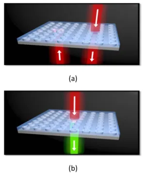
While most conventional nonreciprocal systems are 1D waveguide-type components, extending the realm of such systems to higher dimensions will likely bring a cornucopia of novel physical effects and industrial applications. Metasur-faces, given their combined simple 2D topology and unprecedented capability to transform 3D waves, represent an ideal platform for such developments. Figure 11 shows straightforward applications of nonreciprocal metasurfaces. Early contributions in thisfield include the works reported in [109–118], which will be discussed in the next section.
Current and future challenges. Figure 12(a) represents a
generic nonreciprocal metasurface structure and operation. It differs from reciprocal metasurfaces essentially by the extra presence of TR-breaking mechanism that will be described shortly. Nonreciprocal metasurfaces—as all nonreciprocal systems—may be classified as linear or nonlinear, with the former category further dividing into linear time-invariant (LTI) and linear time-variant (LTV) structures [104]. They
present great potential, but also pose considerable challenges.
We shall only discuss linear nonreciprocal metasurfaces here, whose TR symmetry is broken by a time-odd externalfield F0
[105], called the biasing field, and leave out their nonlinear
counterparts because of their prohibitive limitations, in terms of intensity dependence, one-way-at-time-only operation, and weak nonreciprocity or hysteresis[104].
Figure 11.Conceptual representation of typical applications of nonreciprocal metasurfaces(thick dashed curves) with port n labelled Pn.(a)Planar spatial isolator or nonreciprocal phase shifter. (b)Spherical isolator. (c)Spatial circulator. (d)Transmit-receive radiation pattern discriminator.
Figure 12.(a) Generic representation of a nonreciprocal metasurface, with biasfield F0.(b)Magnetless transistor-loaded ring metamaterial particle, mimicking electron spin precession in ferrites, with current J0operating as the biasingfield [110–112]. (c) Reflective Faraday ring metasurface based on the particle in(b). (Left) Perspective view of the metasurface structure.(Right) Faraday rotation angle versus frequency obtained theoretically from the equivalent magnetic Polder tensor(dashed and solid curves) and experimentally from the prototype shown in the insets(dots) [110].
22
The specification of ports is crucial for the qualification of reciprocity or nonreciprocity. Many asymmetric systems have distinctfield distributions in different propagation directions across the systems while having identical port-to-port ratios, thereby fallaciously appearing nonreciprocal[104].
![Figure 4. (a) The concept of a Huygens’ metasurface [ 38 ]. (b) A loaded strip-loop unit cell [ 40 ]](https://thumb-eu.123doks.com/thumbv2/123dokorg/4635741.41276/10.892.462.822.93.499/figure-concept-huygens-metasurface-loaded-strip-loop-unit.webp)

![Figure 15. (a) THz phase and amplitude modulations achieved by semiconductor-hybridized ETM [ 132 ]](https://thumb-eu.123doks.com/thumbv2/123dokorg/4635741.41276/24.892.461.823.94.502/figure-thz-phase-amplitude-modulations-achieved-semiconductor-hybridized.webp)
![Figure 24. Transmission for the metasurface made up of split ring resonators already studied in [ 187 ].](https://thumb-eu.123doks.com/thumbv2/123dokorg/4635741.41276/35.892.460.820.96.358/figure-transmission-metasurface-split-ring-resonators-studied.webp)
![Figure 28. From [ 207 ]: current distribution and radiation patterns for an elliptical metasurface with size 7.6×5.4 wavelengths](https://thumb-eu.123doks.com/thumbv2/123dokorg/4635741.41276/39.892.87.421.89.349/figure-current-distribution-radiation-patterns-elliptical-metasurface-wavelengths.webp)
