Double Vivaldi antenna for wireless optical networks
on chip
Giovanna Calò1 · Gaetano Bellanca2 · Ali Emre Kaplan2 · Paolo Bassi3 · Vincenzo Petruzzelli1
Received: 9 August 2017 / Accepted: 23 May 2018 © The Author(s) 2018
Abstract In this paper we present a double plasmonic Vivaldi antenna for on-chip optical wireless communication. The proposed antenna is a two-element broadside array fed by a silicon waveguide. The designs of the power splitter and of the hybrid Si-plasmonic cou-pler used for antenna excitation are described in detail. The array radiation characteristics are optimized through Finite Difference Time Domain simulations and the performance of a point-to-point link is evaluated. The proposed double Vivaldi array increases the gain of 3 dB with respect to a single antenna, improving the received power on a link of 6 dB when the double antenna is used for both transmitting and receiving sections.
Keywords Optical antennas · Antenna array · Nanophotonics · Surface plasmons · Wireless optical communications · Optical networks on chip
This article is part of the Topical Collection on Optical Wave and Waveguide Theory and Numerical Modelling, OQTNM 2017.
Guest Edited by Bastiaan Pieter de Hon, Sander Johannes Floris, Manfred Hammer, Dirk Schulz, Anne-Laure Fehrembach.
* Giovanna Calò [email protected]
Vincenzo Petruzzelli [email protected]
1 Dipartimento di Ingegneria Elettrica e dell’Informazione, Politecnico di Bari, Via Orabona, 4, Bari 70125, Italy
2 Department of Engineering, University of Ferrara, Via Saragat, 1, Ferrara 44122, Italy 3 Department of Electrical, Electronic and Information Engineering, University of Bologna, Viale
1 Introduction
Chip Multiprocessors (CMPs), that exploit the potentialities of parallel computing, are the state of the art solution to face the constant need of increasing the computing system efficiency. A CMP consists of several smaller processing cores designed and replicated several times. They achieve performance gain through parallel code execution using mul-tiple threads across the cores. As the number of cores in CMPs continues to scale, the efficient interconnection of these cores is becoming a major challenge, to avoid commu-nication bottleneck and to meet the high bandwidth, low-power and low-latency require-ments which, actually, cannot be matched by traditional point-to-point connections through dedicated wires. Network-on-chips (NoCs) have emerged as a technology enabling a high degree of integration in multi-core systems on chip (Benini and Micheli 2002). The NoCs were introduced to reduce the wiring complexity and to increase communication efficiency by designing regular topologies. However, an important performance limitation in tradi-tional NoCs, which are mainly made by switching elements, network interfaces and inter-switch links, arises from multi-hop communications based on planar metal interconnects and to the consequent high latency and power consumption. In fact, at the physical level, the metal interconnects are responsible for depressing the on-chip data bandwidth while consuming an increasing percentage of power. Different approaches have been investigated to overcome these limitations which range from integrated optics to wireless on-chip com-munication. Architectures based on Optical Network-on-Chip (ONoC) rely on an optical layer, stacked with electronic layers, that allows the communication between different cores in the optical domain (Beausoleil et al. 2008; Shacham et al. 2008; Miller 2009). Opti-cal networks significantly improve electronic technology, but at the expenses of complex layout, sophisticated routing algorithms, and high power budget. Moreover, as the network size scales up, signal losses and crosstalk due to waveguide crossings dramatically increase (Gambini et al. 2015; Fusella and Cilardo 2016; Ortin-Obon et al. 2017). An alternative emerging technology to overcome performance limitations of traditional NoCs is the Wire-less Network-on-Chip (WiNoC), which exploits on-chip wireWire-less transmission to perform an hybrid wired/wireless communication. In this approach silicon integrated antennas replace wired channels, so that transmission performance, power consumption and long distant communication problems of traditional wired NoCs can be addressed simultane-ously (Lin et al. 2007; Ganguly et al. 2011; Deb et al. 2012; Matolak et al. 2012). Recent research has established characteristics of silicon integrated antennas operating in the mil-limeter-wave range of a few tens to one hundred gigahertz to be used for intra- and inter-chip communication. On-inter-chip wireless communication links alleviate not only the latency issues of conventional technologies, but also the topological constraints. As a counterpart, on-chip antennas operating in the millimeter-wave range of a few tens to one hundred giga-hertz suffer for low integrability and are not always viable solution at the CMP communi-cation level; therefore, higher operating frequencies, at least in the THz range, should be required to reduce the size of the radiating elements (Matolak et al. 2012; Lee et al. 2009).
A completely new approach, which can combine the advantages of both the ONoC and the WiNoC, is the on-chip wireless connection through optical nanoantennas. Recent researches have proposed different plasmonic antennas for wireless communication such as dipole and horn antennas (Alù and Engheta 2010; Yang et al. 2016; Merlo et al. 2016; Solís et al. 2013), but the solutions proposed are based on all-plasmonic structures, which do not address the problem of integrating such devices within SOI-based optical networks on chip. In fact, with SOI integrated antennas, the optical signals could be either routed
through waveguides or through wireless links, thus avoiding integration of electronic devices for electro-optical conversions, reducing complexity and energy costs. The elimi-nation of electro-optical conversion has also the potential to guarantee bitrate transparency and distance independence of the photonic links.
The efficient coupling between optical antennas and SOI waveguides is non-trivial, especially when highly directive radiation is required for point-to-point connections. A very efficient coupling between SOI waveguides and plasmonic particle chains was demon-strated in Magno et al. (2016) and Fvrier et al. (2012). These particle chains can behave as directive radiators if suitably designed, but they are characterized by an out-of-plane radia-tion. Hybrid solutions using plasmonic antennas, with hybrid-waveguide feeding (Yousefi and Foster 2012; Yang et al. 2014; Saad-Bin-Alam et al. 2015), have been proposed for wireless applications. However, in order to guarantee a full compatibility with standard optical components, a silicon waveguide feed should be considered. For easy integration between optical wired and wireless connections, in Bellanca et al. (2017) the authors pro-posed a Vivaldi antenna coupled to a silicon waveguide, in which efficient power trans-fer to the antenna is achieved by an hybrid Si-plasmonic coupler. However, to cope with the problem of the high propagation losses due to signal spread (according to the Friis Equation (Kraus 1988), at optical wavelengths the attenuation introduced is of the order of 60 dB for a 100 μm link), some improvements on the antenna performance are needed, to make this approach suitable. Based on the results of Bellanca et al. (2017), in this paper we propose the design of a double Vivaldi antenna, with the aim to improve the gain of both the transmitting and the receiving sections, thus reducing the power budget of an optical wireless link.
2 Double Vivaldi antenna coupled to Si waveguide
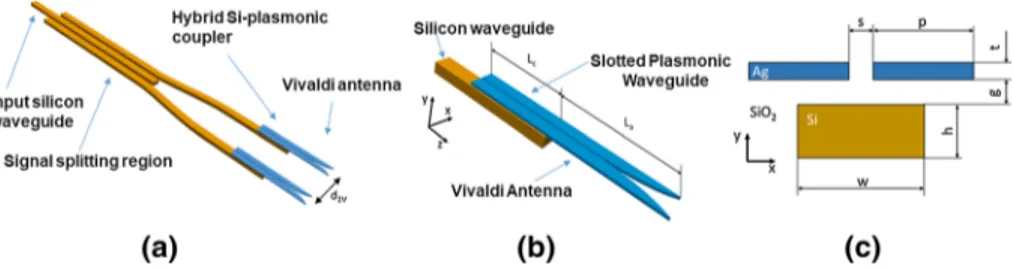
The proposed antenna configuration is shown in Fig. 1a and consists of a broadside array of two Vivaldi radiators fed through silicon waveguides. The excitation of the two antennas is provided by a three-waveguide coupler, which acts as a signal splitter. For a broadside excitation of the array, the signal must be equally split and arrive with the same phase at the two antennas. This is obtained by properly designing the three-waveguide coupler length and by the symmetry of the connections between the the antennas and the coupler ports (see Fig. 1a).
The hybrid Si-plasmonic coupler feeding each element of the array is shown in Fig. 1b, with details of the geometry in Fig. 1c.
Fig. 1 Scheme of the overall double Vivaldi antenna (a), detail of the antenna coupled to the Si waveguide,
In the following sections, we will first consider the design of the hybrid Si-plasmonic coupler, which gives the constraints for the geometrical parameters of both the input signal-splitting region and the antennas. In fact, in order to properly feed the two Vivaldi anten-nas, it is of primary importance to assure an efficient power transfer between the silicon and the slotted plasmonic waveguides. After defining the optimal dimensions for the hybrid coupler, we will describe the design of the signal-splitting region and the optimization of the single Vivaldi antenna. Finally, the optimization of the double antenna array will be addressed.
2.1 Design of the hybrid Si‑plasmonic coupler
In order to design the Si-plasmonic coupler feeding each Vivaldi antenna, the results of the coupled mode theory (CMT) and of the normal mode analysis have been exploited (Yariv 1973; Calò et al. 2012). Although the CMT is not rigorous when strongly coupled waveguides are considered, it can be used to achieve the geometrical design with negligible computational effort, provided the validation with fullwave simulations. According to the CMT, the overall hybrid coupler, shown in Fig. 1c, can be regarded as the superposition of two single waveguides, i.e. the plasmonic slot waveguide and the Si one. To achieve the synchronism condition ( 𝛿 = 𝛽2− 𝛽1= 0 with 𝛽1 and 𝛽2 propagation constants of the
funda-mental modes of the two waveguides when considered uncoupled), the effective refractive indices of the two single structures must be equal. For this purpose, we have chosen to var-iate the width of the two waveguides, i.e. parameter w and p in Fig. 1c. The other geometri-cal parameters are considered as constants and equal to: h = 220 , t = 50 , and g = 80 nm, which are compatible with standard SOI waveguides and fabrication techniques.
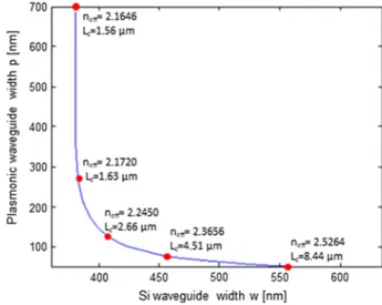
Figure 2 shows the width p of the plasmonic waveguide, which guarantees the synchro-nism condition, as a function on the corresponding Si waveguide width w. In this case, the gap of the slotted plasmonic waveguide is s = 30 nm. Each point (p, w) of this design curve corresponds to possible couples of values of waveguide widths that guarantee the total power transfer between the Si and the plasmonic waveguides. In order to choose among the different possible solutions, we calculated the coupling length Lc , for the different couples Fig. 2 Width p of the plasmonic
waveguide, which guarantees the synchronism condition, as a function on the corresponding
Si waveguide width w. For some
calculation points (red dots), the coupling length Lc and the value
of the effective refractive index
neff of the single waveguides at
synchronism are reported. (Color figure online)
of width values, by evaluating the supermodes (i.e. the normal modes of the overall hybrid-coupler structure) by the Finite Element Method (FEM).1 According to the normal mode
analysis, once verified the synchronism condition, the coupling length Lc can be calculated
as:
where nc1 and nc2 are the effective refractive indices of the first two normal modes of the
overall hybrid coupler. Figure 2 also reports, for some calculation points, the coupling length Lc and the value of the effective refractive index n eff of the single waveguides at
syn-chronism. Higher values of w correspond to lower p values and to longer coupling lengths. In this paper, we have chosen w = 380 nm, p = 270 nm and, therefore, Lc= 1.63 μm .
This configuration is a good compromise that assures a short coupling length without enlarging too much the width of the plasmonic waveguide. In this way, lower losses in the metal and better efficiency of the antenna are expected. Moreover, since the chosen configuration is near to the vertical part of the design curve in Fig. 2, a large tolerance in the choice of p is permitted (by changing p, the synchronism condition is still achieved for almost the same value of w). This condition definitely eases the fabrication process, where the control of the geometry could be difficult.
2.2 Design of the Si three‑waveguide coupler
Provided the Si waveguide dimensions, the design of the three-waveguide coupler for the input signal splitting is straightforward. In fact, the device is a symmetric coupler where all the waveguides are equal. Therefore, in the case of excitation of the central waveguide, the length of the coupler L0 that guarantees an equal splitting of the signal in the two side
waveguides, is given by the following equation:
where n1 and n3 are the effective refractive indices of the first and of the third normal modes
of the three-waveguide coupler. The effective refractive indices of the normal modes of the three-waveguide coupler, calculated by FEM (See footnote 1), are equal to n1= 2.1975 ,
n2= 2.1504 and n3= 2.0967 , respectively. The corresponding optimal coupler length is
L0= 7.69 μm . The coupler length L0 was finally optimized by the Finite Difference Time
Domain (FDTD)2 simulations, to take into account the presence of the curved waveguides,
which are necessary to optimize the distance between the antennas in the two-element array. The calculated optimized length is L0= 7.35 μm.
2.3 Single Vivaldi antenna design
The Vivaldi antenna has been designed by FDTD simulations (See footnote 2). The Vivaldi aperture profile is given by the following equations:
(1) Lc= 𝜆 2(nc1− nc2) (2) L0= 𝜆 2(n1− n3 ) (3) x= c1e Rz+ c 2
1 COMSOL Multiphysics, http://www.comso l.com/.
with
and
where R is the opening rate coefficient, x1 and x2 are the minimum and the maximum x
coordinates of the Vivaldi profile, and, similarly, z1 and z2 are the minimum and the
maxi-mum z coordinates. Here, we report the optimization results obtained by varying the antenna length La for R = 3.0 μm−1 . The other geometrical parameters, such as the width
p of the two metallic strips, their thickness t and the width s of the slot, are constrained by the hybrid Si-plasmonic coupler section. Further details on the antenna design can be found in Bellanca et al. (2017).
The antenna was optimized considering its gain defined as:
where I(𝜃, 𝜙) is the radiation intensity and Pin is the power in input to the Si waveguide.
The radiation intensity I(𝜃, 𝜙) is calculated by the near-to-far-field projection of the FDTD simulated electromagnetic field. The gain is the most significant parameter to optimize the antenna, because it accounts for the radiation efficiency and, therefore, for the losses inside the antenna (either dielectric or conduction losses).
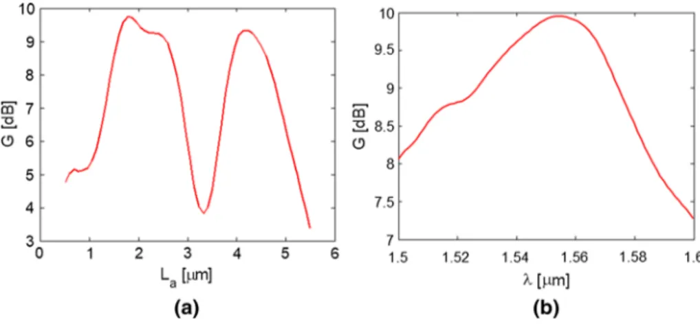
Figure 3a shows the maximum antenna gain as a function of the antenna length La . In
these simulations, we considered only a single antenna fed by its Si waveguide. The results in Fig. 3 were calculated from the gain radiation patterns obtained by the FDTD simulation of the overall structure (i.e. single antenna coupled to the Si waveguide). Standard near-to-far field projections of the fields recorded on a closed box, surrounding the antenna and
(4) c1= x2− x1 eRz2− eRz1 (5) c2= x1eRz2− x2eRz1 eRz2− eRz1 (6) G(𝜃, 𝜙) = 4𝜋I(𝜃, 𝜙) Pin
Fig. 3 Maximum gain of the single Vivaldi antenna (a) as a function of the antenna length La and (b) as a function of the wavelength. In the first plot, R = 3.0 μm−1 and 𝜆 = 1.55 μm . In the second plot,
R= 3.5 μm−1 and L
the input hybrid plasmonic coupler, were calculated once applied Fourier transformations on time-domain FDTD field values (Taflove 2005). The minima and maxima in the gain curve of Fig. 3a are mainly due to resonances in the waveguide-to-antenna connection. In fact, although optimized, the connection is still subject to a residual mismatch which is a function of the structural dimension La . Therefore, the design approach was to choose the
optimal antenna length value La for which the gain is maximum. The optimal gain value
G= 9.9 dB is achieved for La= 1.75 μm . It is worth noticing that, owing to the metal
losses at optical frequencies, the maximum gain is not achieved for longer Vivaldi antennas as would be expected in the lossless case. Figure 3b shows the antenna gain as a function of wavelength for La= 1.75 μm and R = 3.5 μm−1 , which is the optimized value for this
parameter (see Bellanca et al. 2017). A good broadband behavior can be observed, since the gain varies of about 2.5 dB in the whole considered wavelength range (i.e. the C-band).
3 Double Vivaldi antenna radiation characteristics
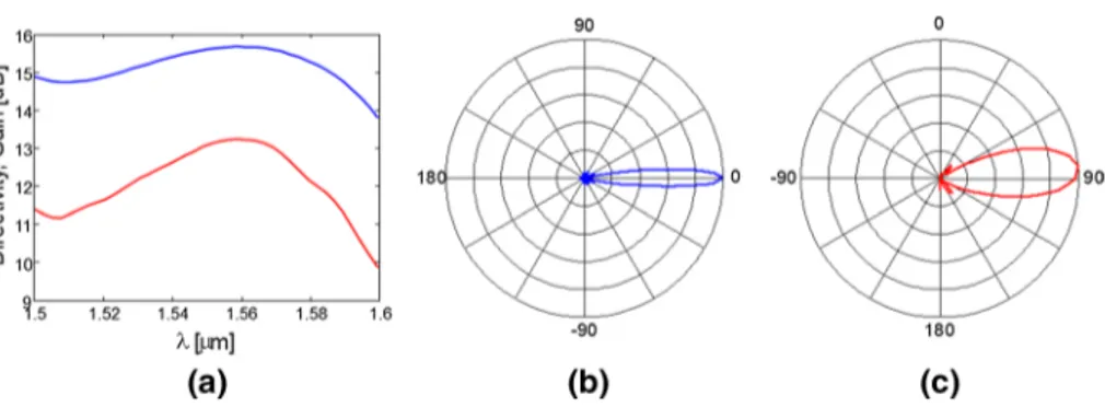
The double Vivaldi antenna behaves as a two-element broadside array in which the two antennas are excited with signals of equal amplitude and phase. As anticipated, this condi-tion is guaranteed by the design of the three-waveguide coupler and by the symmetry of the feeding section. The double Vivaldi antenna was designed and optimized by FDTD as before (See footnote 2). Figure 4a shows the directivity (blue curve) and the gain (red curve) of the double Vivaldi array with center-to-center distance between the antennas d2V = 2.0 μm . This value of the distance between the antennas was chosen by parametric
analysis, with the goal of maximizing the gain of the antenna array. Compared to the single Vivaldi antenna, a 3 dB improvement of the gain is achieved by this configuration.
Figures 4b and c show the double Vivaldi antenna radiation diagrams in the E-plane (horizontal plane) and H-plane (vertical plane), respectively. The aperture angle in the E-plane is 𝜃E= 13◦ and in the H-plane is 𝜃H = 37◦ . Compared to the single antenna, 𝜃E
is reduced of Δ𝜃= 16◦ , whereas 𝜃H remains unchanged, as expected for a linear antenna
array with antennas positioned along the x axis on the xz plane. The results in Fig. 4 were calculated by simulating the overall structure (i.e. input waveguide, signal splitter, hybrid couplers and antennas) and then applying near-to-far field projections to calculate gain and radiation patterns. Therefore, the calculation of the gain takes into account the mismatch
Fig. 4 a Directivity (blue curve) and gain (red curve) of the double Vivaldi array as a function of the
wave-length; in these simulations, the distance between the centers of the two antennas is d2V = 2.0 μm . b E-plane and c H-plane radiation diagrams for the double Vivaldi antenna for 𝜆 = 1.55 μm . (Color figure online)
losses due to the waveguide-to-antenna connection, the losses in the metal, and eventual losses due to the signal splitting region.
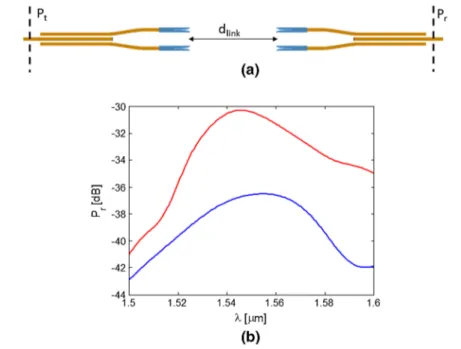
The performance of a wireless link between two double Vivaldi antennas, schematized in Fig. 5a, was evaluated by FDTD simulation. The transmitting and the receiving antennas are positioned at a distance dlink= 50 μm , that verifies the hypothesis of far-field
propaga-tion. An homogeneous surrounding medium, i.e. silica with refractive index nSiO2= 1.44 has been considered in the simulations. The input and the output ports of the link are high-lighted in Fig. 5a. These ports are defined on the Silicon waveguides, respectively, at the transmitter (TX) and at the receiver (RX); they allow to directly compute, through evalu-ation of the power fluxes, the power Pt supplied to the transmitting antenna and the power
Pr collected by the receiver, and therefore to obtain the link power budget. Figure 5b shows the received power Pr for the 50 − μm link with single Vivaldi antennas (blue curve) and
with the double Vivaldi arrays (red curve) at the TX and RX sections, respectively. The transmitted power is Pt= 0.0 dB. As it can be observed, with the two broadside arrays
an improvement of the received power of about 6.0 dB at wavelength 𝜆 = 1.55 μm , is achieved. This result agrees very well with the received power increase that can be pre-dicted by applying the well-known Friis formula for the calculation of the power budget of a wireless link (Bellanca et al. 2017; Kraus 1988).
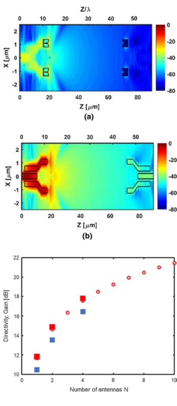
Figure 6 shows the patterns of the electric field intensity |E|2 for the 50 μm optical
link between the two double Viavaldi antennas. In particular, (Fig. 6)a pertains to the horizontal xz plane passing at the center of the metal layer, whereas (Fig. 6b) is for the horizontal xz plane passing at the center of the Si waveguides. The wavelength is 𝜆= 1.55 μm . In Fig. 6a we can clearly notice the effect of the two antenna arrays in the in-plane distribution of the electromagnetic field. Moreover, the decay of the field
Fig. 5 a Scheme of the double Vivaldi antenna link; b received power Pr for the 50 − μm link with single Vivaldi antennas (blue curve) and double Vivaldi antennas (red curve) at the TX and RX sections. The transmitted power is Pt= 0.0 dB. (Color figure online)
Fig. 6 Patterns of the
elec-tric field intensity |E|2 for the 50− μm optical link between the two double Viavaldi antennas:
a horizontal xz plane passing at
the center of the metal layer, b horizontal xz plane passing at the center of the Si waveguides
Fig. 7 Array directivity as
a function of the number of antenna N (red circles), cal-culated according to antenna theory; maximum directivity D (red squares) and gain G (blue squares) calculated by the FDTD, for N = 1, 2, and 4, exciting each waveguide with its fundamental mode. (Color figure online)
intensity with the distance is also apparent. Similarly, in Fig. 6b, we can observe the splitting of the input power in the three-waveguide coupler, and its recombination in the output section.
By increasing the number of antennas, an increase in the directivity and in the gain is expected from antenna theory. In particular, we can calculate the array directivity from the multiplication of the single antenna directivity by the array factor. Figure 7 shows the array directivity as a function of the number of antennas N (red circles), analytically calculated through the array formula. Moreover, we simulated by the FDTD the cases of multiple antennas excited independently in-phase, i.e. without considering the signal splitter, but exciting each waveguide with its fundamental mode. In particular, Fig. 7
reports the maximum directivity values calculated by the FDTD, for N=1, 2, and 4 (red squares). We can see that the FDTD results agree well with the ones obtained from antenna theory (i.e. calculating the array directivity from the multiplication of the single antenna directivity by the array factor). Moreover, from the same FDTD simulations, we calculated the gain for N=1, 2, 4 (blue squares). In all the considered cases, the radia-tion efficiency is 𝜂 = G∕D = 0.7 . It is worth menradia-tioning that, when the signal splitter is included in the simulation, as in the case of N=2, the radiation efficiency reduces to 𝜂= G∕D = 0.6 . Moreover, the signal splitter also induces a reduction of the bandwidth as it can be noticed in Fig. 5b. Therefore, the actual gain of the N element array will be constrained by the performances of the N-ways signal splitting region.
The fabrication of the proposed device will require different steps for the realization of the dielectric waveguides and then of the plasmonic structures. In particular, electron beam lithography (EBL) can be used to fabricate the Si waveguide components (i.e. splitter and waveguides feeding the antennas) on a commercial SOI substrate. After the fabrication of the waveguides and the deposition of the middle dielectric layer, EBL exposure and lift-off techniques can be used to pattern the plasmonic components (i.e. plasmonic coupler and antennas) on the evaporated silver layer.
4 Conclusion
In this paper we have proposed a double Vivaldi broadside antenna array for Optical Wireless Network on Chip applications. The antenna configuration is a two-element array fed by a silicon waveguide. The signal feeding section is made of a three-wave-guide coupler, that behaves as a signal splitter. Moreover, two hybrid Si-plasmonic cou-plers guarantee an efficient excitation of the Vivaldi antennas. This design improves of 3 dB the gain of the single Vivaldi antenna. A point-to-point link has also been simu-lated, showing an increase of 6 dB of the received power with respect to the single antenna configuration. The increased gain makes this configuration suitable to realize longer links for inter- and intra-chip optical communications.
Acknowledgements This research was supported by MIUR through the PRIN 2015 “Wireless Networks
through on-chip Optical Technology—WiNOT” Project and by Apulia region project “Regional laboratory for synthesis and characterization of new organic and nanostructured materials for electronics, photonics, and advanced technologies”. Gaetano Bellanca acknowledges support from “Bando per l’acquisizione di strumenti per la ricerca di Ateneo—Anno 2015” of the University of Ferrara. The research was conducted in the framework of the project Galileo 2018 G18-625/ PHC Galile 39622NL.
Open Access This article is distributed under the terms of the Creative Commons Attribution 4.0
Inter-national License (http://creat iveco mmons .org/licen ses/by/4.0/), which permits unrestricted use, distribution, and reproduction in any medium, provided you give appropriate credit to the original author(s) and the source, provide a link to the Creative Commons license, and indicate if changes were made.
References
Alù, A., Engheta, N.: Wireless at the nanoscale: optical interconnects using matched nanoantennas. Phys. Rev. Lett. 104, 213902 (2010). https ://doi.org/10.1103/PhysR evLet t.104.21390 2
Beausoleil, R.G., Kuekes, P.J., Snider, G.S., Wang, S., Williams, R.S.: Nanoelectronic and nanophotonic interconnect. Proc. IEEE 96(2), 230–247 (2008)
Bellanca, G., Calò, G., Kaplan, A.E., Bassi, P., Petruzzelli, V.: Integrated Vivaldi plasmonic antenna for wireless on-chip optical communications. Opt. Express 25, 16214–16227 (2017)
Benini, L., Micheli, G.D.: Networks on chips: a new SoC paradigm. Computer 35(1), 70–78 (2002) Calò, G., D’Orazio, A., Petruzzelli, V.: Broadband MachZehnder switch for photonic networks on chip. J.
Lightw. Technol. 30, 944–952 (2012)
Deb, S., Ganguly, A., Pande, P.P., Belzer, B., Heo, D.: Wireless NoC as interconnection backbone for mul-ticore chips: promises and challenges. IEEE. J. Emerg. Sel. Topic Circuits Syst. 2(2), 228–239 (2012) Fusella, E., Cilardo, A.: Crosstalk-aware automated mapping for optical networks-on-chip. ACM Trans.
Embedded Comput. Syst. 16(1), 16.1–16.26 (2016)
Fvrier, M., Gogol, P., Aassime, A., Mgy, Rt, Delacour, C., Chelnokov, A., Apuzzo, A., Blaize, S., Lourtioz, J., Dagens, B.: Giant coupling effect between metal nanoparticle chain and optical waveguide. Nano Lett. 12(2), 1032–1037 (2012)
Gambini, F., Faralli, S., Pintus, P., Andriolli, N., Cerutti, I.: BER evaluation of a low-crosstalk silicon inte-grated multi-microring network-on-chip. Opt. Express 23(13), 17169–17178 (2015)
Ganguly, A., Chang, K., Deb, S., Pande, P.P., Belzer, B., Teuscher, C.: Scalable hybrid wireless network-on-chip architectures for multicore systems. IEEE Trans. Comput. 60(10), 1485–1502 (2011)
Kraus, J.D.: Antennas, 2nd edn. McGraw-Hill, Maidenherd (1988)
Lee, S.-B., Tam, S.-W., Pefkianakis, I., Lu, S., Chang, M.F., Guo, C., Reinman, G., Peng, C., Naik, M., Zhang, L., Cong, J.: A scalable micro wireless interconnect structure for CMPs MobiCom’09. In Pro-ceedings of the 15th Annual Int. Conf. on Mobile Computing and Networking, 217–228, (2009) Lin, J., Wu, H., Su, Y., Gao, L., Brewer, J.E., O, K.K.: Communication using antennas fabricated in silicon
integrated circuits. IEEE J. Solid-State Circuits 42(8), 1678–1687 (2007)
Magno, G., Ecarnot, A., Pin, C., Yam, V., Gogol, P., Mgy, R., Cluzel, B., Dagens, B.: Integrated plasmonic nanotweezers for nanoparticle manipulation. Opt. Lett. 41(16), 3679–3682 (2016)
Matolak, D.W., Kodi, A., Kaya, S., Di Tomaso, D., Laha, S., Rayess, W.: Wireless networks-on-chips: archi-tecture, wireless channel and devices. Wireless Commun. 19(5), 58–65 (2012)
Merlo, J.M., Nesbitt, N.T., Calm, Y.M., Rose, A.H., D’Imperio, L., Yang, C., Naughton, J.R., Burns, M.J., Kempa, K., Naughton, M.J.: Wireless communication system via nanoscale plasmonic antennas. Sci. Rep. 6, 31710-1–31710-8 (2016)
Miller, D.B.: Device requirements for optical interconnects to silicon chips. Proc. IEEE 97(7), 1166–1185 (2009)
Ortin-Obon, M., Tala, M., Ramini, L., Vinals-Yufera, V., Bertozzi, D.: Contrasting laser power requirements of wavelength-routed optical NoC topologies subject to the floorplanning, placement and routing con-straints of a 3D-stacked system. IEEE TVLSI 25(7), 2081–2094 (2017)
Saad-Bin-Alam, M., Khalil, I., Rahman, A., Chowdhury, A.M.: Hybrid plasmonic waveguide fed broadband nanoantenna for nanophotonic applications. IEEE Photon. Technol. Lett. 27(10), 1092–1095 (2015) Shacham, A., Bergman, K., Carloni, L.P.: Photonic networks-on-chip for future generations of chip
multi-processors. IEEE Trans. Comput. 57(9), 1246–1260 (2008)
Solís, D.M., Taboada, J.M., Obelleiro, F., Landesa, L.: Optimization of an optical wireless nanolink using directive nanoantennas. Opt. Express 21(2), 2369–2377 (2013)
Taflove, A.: Computational electromagnetics: the finite-difference time-domain method. Artech House, Bos-ton (2005)
Yang, Y., Zhao, D., Gong, H., Li, Q., Qiu, M.: Plasmonic sectoral horn nanoantennas. Opt. Lett. 39(11), 3204–3207 (2014)
Yang, Y., Li, Q., Qiu, M.: Broadband nanophotonic wireless links and networks using on-chip integrated plasmonic antennas. Sci. Rep. 6, 19490-1–19490-8 (2016)
Yariv, A.: Coupled-mode theory for guided-wave optics. IEEE J. Quantum Electron. QE–9(9), 919–933 (1973)
Yousefi, L., Foster, A.C.: Waveguide-fed optical hybrid plasmonic patch nano-antenna. Opt. Express 20(16), 18326–18335 (2012)