Universit`a degli Studi di Pisa Facolt`a di Ingegneria
Corso di Laurea Specialistica in Ingegneria Elettronica
VLSI-design and FPGA-based prototyping of a buffered serial port for audio applications
Relatori:
Primo relatore Prof. Luca Fanucci Secondo relatore Prof. Pierangelo Terreni Terzo relatore Ing. Sergio Saponara
Candidato: Andrea Marini
Ringraziamenti
Questa tesi ´e stata svolta durante uno stage di cinque mesi presso StarCore Llc, nella sede di Austin, in Texas. I primi ringraziamenti vanno quindi al Professor Fanucci e all’Ingegner Saponara per aver reso possibile questa esperienza ed avermi assistito da oltreoceano.
La mia gratitudine va poi a chi mi ha seguito indefessamente durante questo lavoro, il mio mentore Andrew Temple: da lui ho potuto imparare molto in quanto a metodo e dedizione.
Una menzione speciale va alla truppa italiana che mi ha accompagnato in questa speciale avventura; grazie per tutto l’apporto dato ad un disgraziato stampellante, per la pazienza alle mie domande e per non avermi fatto morir di fame.
Non ci sono proprio parole per tutte le persone che mi sono state vicine in questi anni, a Scuola, a ingegneria, a ISF, in Erasmus, a Brescia e a Pisa. Se sono arrivato fino a questo punto ´e soprattutto grazie a tutti voi.
Non dimentico certo la mia famiglia che mi ha sempre sostenuto, ac-colto e stimolato nelle mie peripezie e nei miei irrequieti ritorni sotto il tetto materno.
un grazie immenso a tutti quanti
Contents
1 Ringraziamenti 2
I
First part
10
2 The System-on-Chip and the Design Reuse 11
2.1 From the Printed Circuit Board to the System on Chip . . . . 11 2.2 Intellectual Property Cells in Digital Design . . . 13
3 Digital Signal Processors 15
3.1 An introduction to Digital Signal Processors . . . 15 3.2 How to evaluate a DSP processor performance . . . 20 3.2.1 Traditional Approaches: MIPS, MOPS and MACS . . 20 3.2.2 Application Benchmarking and Algorithm Kernel
Bench-marking . . . 21 3.3 How to Develop an Application for a DSP Processor . . . 22
II
Second part
25
4 Introduction to the system 26
4.1 Analysis of the Problem . . . 27 4.2 The Resources . . . 29 4.3 The Constraints: the Software Compatibility . . . 32
CONTENTS
5 The Design Flow and the Solution Description 34
5.1 The Design Flow . . . 34
5.2 Description of the solution . . . 37
III
Third part
41
6 The User FPGA System Design and Implementation 42 6.1 The FPGA system architecture and flow of work . . . 436.1.1 The implementation flow . . . 44
6.2 The System Bus Slave and Decoder . . . 45
6.3 The User FPGA Control Register . . . 47
6.4 AHB Off-Chip DMA Bus Master . . . 49
6.5 The Audio Port Interface . . . 49
6.6 The issue of synchronous design . . . 51
7 The Audio Port Controller 53 7.1 The Audio Port Controller Design Flow . . . 53
7.2 The Architecture of the Controller . . . 54
7.3 Input-output model . . . 56
7.4 The control part . . . 56
7.4.1 The Instruction Set . . . 58
7.4.2 The phases of each instruction . . . 61
7.4.3 The execution phase . . . 61
7.4.4 The Address Generation Unit . . . 62
7.4.5 The Interrupt Control Unit . . . 63
7.4.6 The Interrupt Generator Unit . . . 64
7.5 The program memory . . . 64
7.6 The DEBUG mode . . . 65
7.7 The Controller Mapped in the FPGA . . . 65
8 The Software 67 8.1 Introduction . . . 67
CONTENTS
8.2 The Audio Port Driver . . . 68
8.2.1 Data structures . . . 68
8.2.2 Interrupt Service Routine Data Variables . . . 70
8.2.3 Audio Port Driver Functions . . . 71
8.3 The Interrupt Service Routine . . . 71
8.3.1 The Audio Port Configuration . . . 72
8.3.2 The Transfer Section of the ISR . . . 73
8.3.3 The Control Section of the ISR . . . 73
8.3.4 Changes made in the ISR . . . 74
8.4 The Program Running on the Controller . . . 74
9 Achievements 79 9.1 The Adaptive Multi-Rate Vocoder . . . 79
9.2 The Evaluation of Performance . . . 81
IV
Appendixes
84
A AMBA AHB Bus description 85 A.1 The Architecture . . . 85A.2 The Signals and the Timing . . . 87
A.2.1 The Endianness . . . 87
B The Audio Port Integrated Circuit 91
C Verilog appendix 94
D Glossary 98
List of Figures
3.1 DSP application design flow . . . 23
4.1 DMA and ISR . . . 28
4.2 Overview of the DB1000 . . . 31
5.1 Design flow block diagram . . . 36
5.2 System solution overview . . . 39
6.1 Description of the FPGA system . . . 43
6.2 Audio Port Interface . . . 52
7.1 Internal architecture of the audio port controller . . . 55
8.1 Variables in the internal memory . . . 78
9.1 Wireless transmission block diagram . . . 80
9.2 Human speech model . . . 81
A.1 Architecture of AHB bus system . . . 86
A.2 AHB signals overview . . . 88
A.3 Example of AHB timing for a write operation . . . 89
A.4 Active byte lanes for a 32-bit little endian bus . . . 90
A.5 Active byte lanes for a 32-bit big endian bus . . . 90
Introduction
The present market of semiconductor is very competitive; on one side con-sumers ask for always increasing performance and new possibilities, on the other companies have to offer low prices in order to be successful. For what concerns performance just think of the wide range of mobile applications, such as PDAs, cellular phones, and laptops : quality of services, duration of the battery and computational power are always taken into account when buying new devices. On the other side, due to the competition, costs have to be very low; this means that both recursive and non-recursive engineering costs have to be kept under control.
Time is another important concern: it is usually true that the earlier a product is presented to the market, the wider share of the market it will gain. This leads modern semiconductor companies to look for viable ways to design improved products in a short time. Because of the complexity of the new electronic systems, this is not an easy task to be accomplished; even tough electronic design automation (EDA) tools have greatly improved in the recent years, a gap still exists between the rate foundries can produce chips and the rate these chips can be designed.
A very common approach to deal with complexity and performance re-quirements is to integrate as many functions as possible on a single chip (System-On-Chip); this allows higher clock frequency and lower costs. In connection to this also design reuse has spread in a great part of semicon-ductor world. This means using in your system modules that others have already designed and tested. This allows you to skip some steps in the
de-sign flow (at least for those modules) and saving a de-significant amount of time.
In this framework lies the work of my thesis, developed at the StarCore, a company headquartered in Austin, Texas. StarCore designs and licences Digital Signal Processors as intellectual property; this is basically one of the companies that offer its product to be used in other electronic systems, avoiding licensees to spend time in designing it by themselves.
A Digital Signal Processor is a special kind of processor, designed to execute calculus-intensive applications: encoding and decoding of informa-tion, voice synthesis and recogniinforma-tion, compression and decompression of data, Fourier Transform are just some examples. In many systems, thanks to its programmability and its limited cost it is the suitable solution. For example most mobile phones employs a DSP processor to perform base band operation on the signal.
In these kind of systems, it is important that very few cycles are spent doing other than signal processing, such as dealing with peripherals. In the case of an audio signal it is important that the audio port asks for the fewer cycle it is possible. For this reason at StarCore my activity was to design and develop an audio port controller aiming to reduce at least the cycles asked to the processor in case that the algorithm run is frame based.
For this purpose I designed hardware to be mapped into an FPGA, and wrote some software for the DSP; I worked mainly with the Development Board, used to prototype applications based on the StarCore processor.
The first part of my thesis introduces some concepts of the modern semi-conductor world that I consider important in order to understand the envi-ronment my work was developed. They are System-On-Chip, Design Reuse and Intellectual Property. Besides those concepts I added an introduction to the important technology of Digital Signal Processor.
In the second part of this report there is an introduction to my activity at StarCore: the problem I faced, the resources available, the constraints, an overview of the solution, and the design flow I used.
In the third part there are all the details of the implementation: the architecture of the User FPGA, the details of the audio port controller and some final considerations on the achievements.
In the appendix I considered useful to provide further details on the AHB standard for On-Chip Buses and to show some meaningful part of the Verilog Code I wrote.
Part I
First part
Chapter 1
The System-on-Chip and the
Design Reuse
Nowadays System-On-Chip and Design Reuse are two of the dominant paradigms in the digital electronic world; in the chapter I would like to introduce both of them trying to focus on their importance in the present semiconductor world.
1.1
From the Printed Circuit Board to the
System on Chip
Integration is a key concept to understand the evolution of electronic system from the very beginning up to now. In the early days every single device was produced by itself and to create a simple system every component was soldered on a board and connected to the others by wires. On the contrary nowadays very large systems are created on a single chip, that is millions of transistors on the same little piece of silicon. This is the result of the integration, and I’ll try to explain this process in order to understand the present panorama of the semiconductor world.
The first Integrated Circuit was born approximately in the late 50’s, in Fairchild and Texas Instruments where they succeeded in producing resistors,
1.1 From the Printed Circuit Board to the System on Chip
capacitors, transistors and diodes on the same slice of silicon. Thanks to this technological improvement the concurrence of vacuum tubes was beaten and the semiconductor industry stopped to be an uncertain but promising reality to became the ever-growing industry that we know today.
In the 70’s Large Scale of Integration (LSI) allowed to produce complex systems such as memories, micro-controllers and microprocessors; the pro-duction spread from the U.S. to Europe and other country in East Asia, such as Japan, South Korea and Taiwan.
During the 80’s the driving applications were the Personal Computer and other home electronic appliances. The former is important because to it applies the paradigm called Printed Circuit Board (PCB). In fact the best example of PCB is the PC’s motherboard: it is a board made of plastic material where the processor, the memory and all the other modules can be soldered and interconnected.
So the Printed Circuit Boards were the ground for electronic systems; they allowed the integration of chips very different from each other, with ad-hoc multi-layered connections. In this way many chips from different vendors and with different functions could be assembled together in a single system. In the 90’s finally came a new degree of integration: the System-On-Chip. As the name suggests, a SoC is a complete system that stands on a single slice of silicon in a single package. Many parts of an electronic system have been integrated, thanks to both the miniaturization of devices and the improvement of design tools. On the one hand this means higher allowed frequencies, lower consumption and less silicon area, but on the other hand there is an increased complexity that causes risks and costs.
To face this problem and to keep the complexity to a manageable size, design reuse techniques were introduced; system designers were given the possibility to integrate previously designed modules. This is the subject of the next section.
1.2 Intellectual Property Cells in Digital Design
1.2
Intellectual Property Cells in Digital
De-sign
The design of a System-On-Chip is one of the most challenging activity in the modern era of semiconductor. Since SoCs offer so many positive features, many industry and research groups are doing many efforts in order to face this problem; in particular one of their goals is to provide designers with automatic tools that guarantee a successful output in a short time and at low cost.
As introduced before, one of the main issues in SoC design is the great complexity of such systems. Just imagine you have to deal with a CPU, a memory, and a number of peripheral in the same project; you could desire to describe them in HDL, simulate them, produce their logic synthesis, always considering them as a single unit. This is clearly demanding and it takes a lot of time.
When SoCs started to spread in the semiconductor world, it was intro-duced the idea of including in SoC project some parts that had been already designed and verified. For example instead of describing from scratch a controller that you would need in your system you could use a micro-controller already designed by a third-party company. This latter sells you the Intellectual Property of that module, that is usually a RTL model fully tested and verified. By paying this company you get the right of employing their knowledge and you are quite sure that you don’t have to worry about the implementation of that module but just on its integration in the system. One of the most successful example of Intellectual Property design pro-duction was ARM; this English company in the early 90’s offered to the market a soft micro-controller, that was easily integrated in many embedded SoCs. After this example proved that design reuse was a viable way in the semiconductor industry, many other companies started to provide different blocks with different features.
Intellectual Property vendors basically design their own products, test
1.2 Intellectual Property Cells in Digital Design
them, and try to synthesize them on different fabrication technologies. One of the key concepts (and strength) of design reuse and intellectual property is their technology independence; notwithstanding for SoC designers any aid in any phase of the design is welcome, in particular in the logic synthesis.
So nowadays design reuse is very wide spread, there are many IP vendors and many designers integrates more and more massively soft modules in their chips; far from being a direct solution to the SoC design it is anyway a very important help in keeping the complexity low and the prices affordable.
Chapter 2
Digital Signal Processors
This chapter introduces the technology I worked with: Digital Signal Proces-sors. A DSP processor was the core of the system I developed so an overview on this kind of devices is necessary. In the first section I describe the archi-tecture and the feature of the DSP processors; in the second section I provide some methods of evaluating the performance of such processors, while the last section deals with the application design flow, another important key in my work.
2.1
An introduction to Digital Signal
Proces-sors
The function of a great part electronic systems is to process the information that could come from the environment or from other similar systems. One possible way to classify them is by their degree of programmability; at the bottom of this classification we find dedicated systems such as Application Specific Integrated Circuits (ASIC). These are designed to perform a single task; it could also be very complex but it will be the same for the whole device’s life. Instead on the top we find the processors that with the aid of a memory, could perform any desired task.
2.1 An introduction to Digital Signal Processors
that are the hearth of every PC and laptop. If we go down from there, we immediately find two other kinds of processor: microcontrollers and Digital Signal Processors (DSP). They both are generally simpler than GPPs, but nevertheless they can still do almost everything. If we accept the general di-vision of processor instructions in control instructions and arithmetic-logical instructions, we could say that the former is specialized in control instruc-tions, while the second is focused on AL instructions.
Both kinds of processor are used in a number of applications, either be-cause the high performance of GPPs would be unused or bebe-cause the available resources (namely money,power and frequency) are not enough for a GPP. In systems where there are many peripherals and the task are computationally easy the most suitable processor is the microcontroller; if on the other side we require high calculus capacity the straightforward choice is the DSP.
As the name suggests the DSP is particularly suitable for the elaboration of signals, like audio and video signals. DSPs appeared for the first time in the early 80’s, when Texas Instruments designed a processor specialized for operations like Finite Impulse Response (FIR) filter, and Fourier Transform (FT). The core of both these operations is the so-called tap that consists of a multiply and an accumulate operation linked together. These could have been completed without any concerns by a GPP but it would have taken a huge number of instructions, maybe failing to follow the signal and hence loosing information; consider that at that time no GPP had a multiply unit and most of them had a single access to memory. Multiplication was performed by adding and shifting as many times as the width of the data! Also take into account that a FIR algorithm requires two operands (the signal sample and the response coefficient) each time; this means two accesses in the memory for the data (besides program memory accesses), and given the intrinsic slowness of memories all this leaded a big loss of cycles.
For these reasons two were the main features introduced:
new memory architecture the so-called Harvard architecture was de-ployed, where the processor could access separately and at the same 16
2.1 An introduction to Digital Signal Processors
time the program memory and the data memory;
multiply unit in the execution unit a module was dedicated to the multi-plication.
The price to pay was an increased complexity and more hardware (more area and more power consumption), but this made a single-cycle multiplica-tion possible and an on-line execumultiplica-tion of those algorithms reliable. Notwith-standing those drawbacks, this new system proved to be extremely cost-effective, and DSP’s use rapidly spread in the semiconductor world.
In late 80’s and in the 90’s many other innovations were introduced in the DSPs’ architecture: among them the introduction of the Very Long Instruc-tion Word (VLIW), of the Single InstrucInstruc-tion Multiple Data (SIMD) and an high degree of parallelism. All these improvements lead to the wide range of DSPs that nowadays we can find in the semiconductor market: from the DSP for high fidelity home audio systems where high precision is required, to the DSP for mobile applications where the limited power and cost are the most important requirements.
In the following I would like to introduce the innovative concepts of VLIW and SIMD that are commonly used in the design of high-performance DSPs. The Very Long Instruction Word architecture One way to dramat-ically increase the performance of a DSP is to use multiple execution units (EU) in parallel; this means that you can at first fetch and then execute multiple instructions at the same time. This obviously leads to an increased complexity and there are different techniques to deal with it, that are VLIW and superscalar architecture.
The basic problem is to choose which instruction is executed in which EUs; this choice could be done either on-line by the processor itself or by an ad-hoc compiler. The former solution is adopted in the superscalar processors and the price to pay is an increased complexity of the execution part. The opposite approach is found in the VLIW DSP; in this case the load of the choice is carried by the compiler that groups the instructions in execution 17
2.1 An introduction to Digital Signal Processors
sets according to some rules. The positive feature of this approach is that
notwithstanding an high degree of parallelism (up to eight instructions in parallel) the complexity ( and so delay and power consumption) keeps low. The Single Instruction Multiple Data SIMD is an architectural tech-nique that could be used within any class of architectures. SIMD improves performance of DSP processor, by allowing it to execute multiple instances of the same operation in parallel using different data.
SIMD operations could be implemented in hardware with two basic tech-niques; the first is by adding a second set of execution units that exactly duplicates the original set. The second is based on the idea of splitting the DSP execution units into multiple sub-units that process narrower operands. Both this solutions are used extensively in the TigerSHARC DSP ar-chitecture from Analog Devices. This processor for example is capable of executing eight 16-bit multiplications per cycle.
After this overview of the short history and major developments in the DSP field, in the last part of this chapter I am going to point out and other interesting features to provide a complete picture.
efficient memory access As I mentioned earlier the memory architecture is as important as the DSP core; digital processing requires very high memory bandwidth but offers advantages like predictability and very intense code repetition. Therefore while on one side it requires at least two buses, one for instruction the other for data, on the other side it allows intensive use of program cache and particular addressing modes. data format Most DSP processors use a fixed-point numeric data type in-stead of the floating-point format most commonly used in scientific application. This means that the binary point is located at a fixed lo-cation in in the data word. Floating-point formats allow a much wider range of values to be represented, and highly reduce the risk of over-flow; moreover DSP applications require a high numeric fidelity that 18
2.1 An introduction to Digital Signal Processors
is difficult to be maintained in fixed-point representation. The reason why the fixed-point is so common is that there are other more impor-tant constraints in DSP systems such as cost and energy efficiency. For these goals fixed-point format is far better than its counterpart, being its hardware implementation simpler and cheaper. Another point in data format is the data word width: DSP processors tend to use the shortest data word width that provides the adequate accuracy in their target applications. So most fixed-point DSP processors use 16-bit data words. In such cases in order to ensure adequate signal quality some hardware is added, like wider accumulator register to hold the result of summing several multiplication products.
zero-overhead looping DSP algorithms usually spend most of the process-ing time executprocess-ing a short part of the code, that are run continuously, i.e. loops. To improve the performance DSP processors provide spe-cial hardware to support looping, in updating and checking the loop counter and in the branching back to the top of the loop.
specialized instruction set DSP processors instruction sets usually present two features: they make the maximum use of the underlying hardware by being highly parallel, and they have quite short instructions. This results in wide and complicated sets of short and specialized instruc-tions. The shortness of each instruction is very important in keeping the amount of the program memory low, but it has heavy drawbacks such as an increased number of instruction and a reduced sets of em-bedded registers. Thus it is easy to understand that programming such DSP processors is not a trivial task; moreover very rarely high-level lan-guage compilers like C compilers produce an optimized assembly code that deploys all the feature of the processors. This is why most of the code of in DSP applications (or at least the most calculus intensive parts) are written directly in assembly language by DSP programmers.
2.2 How to evaluate a DSP processor performance
2.2
How to evaluate a DSP processor
perfor-mance
After this short overview of the architecture and of the features of the Digital Signal Processors I consider important to talk about the way of evaluating the performance of such systems. This is useful for designers in order to choose to most suitable devices given some constraints. DSP processor per-formance can be measured in many ways; the first is surely the execution time, that is the time taken to accomplish a defined task. Others are the power consumption and the memory usage. The following sections describe different metrics, trying to point out the strength and the weakness of every method.
2.2.1
Traditional Approaches: MIPS, MOPS and MACS
The metric that is traditionally used is MIPS, that stands for Millions of In-structions Per Second. This is a simple counting of the number of inIn-structions executed in a definite amount of time. This kind of measurement is mislead-ing because it strongly depends on the architecture of the DSP; for example a device with powerful execution units could perform a complex mathemati-cal operation in a single instruction. This would cause a low MIPS, because the execution of that instruction could take longer than execution of simpler ones.On the other side a DSP with very simple instructions could score a very high MIPS, even if the actual mathematical operation are very few. Anyway MIPS is valid within the context of a single known processor architecture.
To avoid that confusion, other metrics have been used such as Millions of Operations Per Second (MOPS) and Multiply-Accumulates Per Second (MACS). Nevertheless they both proved to be unfair. The problem with MOPS is related to the difficulty of defining an operation, everyone using its own concepts. For what is concerning the MACS, the point is that even if the MAC is an important operation, in DSP algorithms involve many other operations than this. This makes it not reliable as an overall evaluation 20
2.2 How to evaluate a DSP processor performance
parameter.
Anyway neither MIPS,MOPS nor MACS address other fundamental is-sues in DSP performance evaluation like memory usage and power consump-tion. Just think of a very high MIPS DSP processor that has slow memory access or of a system with high consumption of memory requiring the use of slower external memory; in both cases the MIPS of the processor would never been deployed since the memory bandwidth would a serious bottleneck. Also the evaluation of power consumption could be an issue since it is strongly affected by the frequency and by the kind of instructions executed.
For these reasons other metrics have been developed in order to provide DSP system designers with more reliable metrics.
2.2.2
Application Benchmarking and Algorithm
Ker-nel Benchmarking
As I said above, in order to take account of every issue, it is more use-ful to consider a system perspective. In this case a possible approach is theapplication benchmarking; this means running on the DSP system an ap-plication or even a suite of apap-plications and measuring time, memory usage and energy consumption. This method has its own limits too; in fact applica-tions are usually written in high-level language like C, and the benchmarking output will also include an evaluation of the compiler or of the programmer’s skills.
Hence it’s necessary to make one step down to reach the most suitable DSP performance evaluation method, that is algorithm the algorithm kernel
benchmarking. Far from being perfect and complete, it is nevertheless the
most common method used to compare different DSP devices and architec-tures.
Algorithm kernels are the building blocks of most signal processing sys-tems and include functions such as fast Fourier transforms, vector additions and multiplications, and filters. These have some compelling advantages such as ease of specification, optimization and implementation; this means that 21
2.3 How to Develop an Application for a DSP Processor
they could be identified easily, implemented in a short time in assembly code and you can be quite sure that your implementation is close to the optimum one. Thus a set of algorithm kernels has been selected and it is commonly used to evaluate the performance of the each DSP.
Typical examples of benchmark suites are offered by the EDN Embedded Micro-processor Benchmark Consortium (EEMBC), that could also be used for DSP Processors. EEMBC develops different suites of benchmarks for different fields, such as consumer, networking, telecom, automotive and office automation. Each suite is composed of a range (five to sixteen) of individual benchmark tasks representative of that product category; for example in the consumer category you could find algorithms for image compression, image filtering, color conversion and other tasks common to consumer digital imaging products.
In this way companies can have a standard evaluation of their processor, that could be compared with those of their competitors.
2.3
How to Develop an Application for a DSP
Processor
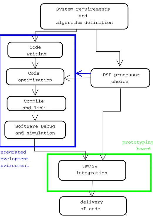
After this introduction of the DSP processor, the next step is to describe how to develop an application on a DSP platform. This is more closely related to my activity at StarCore; I will underline the role of the Development Board that is the platform I worked with.
As you can see in picture 3.1 the beginning step is the definition of the requirements of the system, and the definition of the algorithm to be imple-mented. These greatly affects the choice of the processor and the architecture of the system.
Once the device has been chosen, the designer is provided by the DSP vendor with a suite of software tools that are really helpful in the develop-ment; these includes a compiler, a linker, a DSP processor simulator and a profiler. The latter is used to understand which part of the program is more 22
2.3 How to Develop an Application for a DSP Processor System requirements and algorithm definition Code writing Code optimization Compile and link Software Debug and simulation HW/SW integration DSP processor choice integrated development environment prototyping board delivery of code
Figure 2.1: DSP application design flow
2.3 How to Develop an Application for a DSP Processor
intensively run, that is the part the programmer should optimize best. The processor simulator is a great tool too; it allows the program to be run and performance evaluated. It has some drawbacks: first of all it’s very expensive to be built and secondly it is easily overcome by an hardware simulation in terms of speed and computation resources.
For these reasons -where possible- the hardware simulation is preferred; it could be done thanks to a Prototyping Board, where a system similar to the target one could be created. It is a Board delivered by the DSP vendor that could be customized by the DSP programmer in order to test the program and the whole system in the proper conditions.
On this kind of boards there is the DSP processor, so the code could be downloaded from the PC where it has been developed and made it run on the actual platform. An important feature that is usually on the same chip as the processor is the Emulator, that allows the programmer to control the flow of the program from the IDE, doing an efficient debugging. In general using the Prototyping Board allows to test in a quite easy way not only the DSP core but also all the systems resources like memories, caches, buses and peripherals. For these reasons this is a necessary step in the development of applications especially for such a particular systems like DSP systems.
This is an overview of the design flow for a DSP application; in my work at StarCore I mainly focused on this las part, since I worked on the Development Board DB1000 that is the Prototyping Board used for the StarCore processor. A deeper description of this board is in the next chapter, together with a complete introduction to my work in StarCore.
Part II
Second part
Chapter 3
Introduction to the system
The activity is basically the design and the implementation of a controller for an audio port. An audio port is a simple device to collect and play audio signals; on one side you have a microphone or a speaker, on the other you have digitally represented samples. This kind of device is used in every applications where sound is involved; for example a mobile phone has an audio port to record and reproduce the voice in a conversation. Like many other peripherals the audio port communicates to the CPU of the system with the interrupt mechanism. This is a typical method of communication but not always it is suitable for the correct deployment of the system resources. This is particularly true in a DSP system, where every cycle should be spent on algorithm processing, and where algorithms usually are frame-based. Hence in my work at StarCore was the need for a module - a controller - between the audio port and the DSP processor, that implements a buffer mechanism, in order to interrupt the core just once per frame instead of every sample.
So the first section of this chapter tries to provide an overview on possible solutions in order to deal with peripherals in a DSP environement. On the other hand the section after describes the actual system I worked with, that is the Development Board, an important tool already named in the previous chapter. Then as a conclusion of this chapter there is a section dedicated to the constraints I had in the implementation of the controller.
3.1 Analysis of the Problem
3.1
Analysis of the Problem
As briefly introduced above the communication between a DSP processor and the peripherals of the system could be an issue for the designers and the users. In particular there is the risk of loosing all the advantages of a DSP processor if the peripherals are not managed in an appropriate manner.
This could happen when the processor elaborates sets of values all to-gether and not single samples; this is the case of some audio algorithms and most video and picture processing operations. If you think at the video case it is easily understandable that the elaboration is usually done on the complete frame and not on the single pixels.
So if the processor is asked to stop at every incoming samples just to transfer it in the internal memory, this would be a great lost of cycles. Every cycle spent by the processor in tasks other than signal processing is considered
overhead, a necessary price that you try to minimize; so the main goal of my
activity is to reduce the overhead in the communication between the DSP and the audio port.
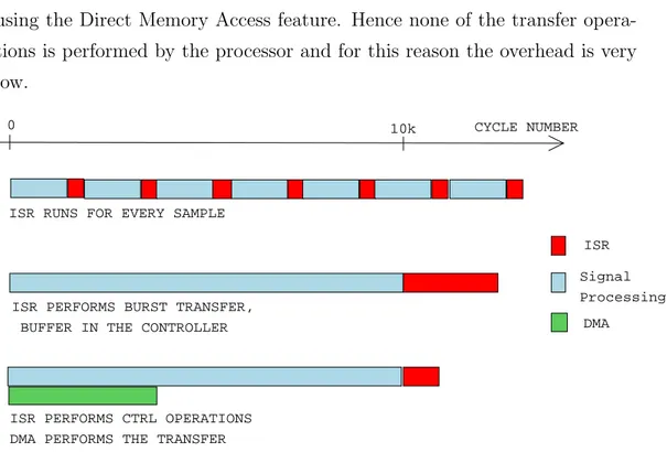
Even if the interrupt mechanism is a very used one and it works very well in most of cases, sometimes other solutions can guarantee far better performance; the Direct Memory Access (DMA) is one of them: it is a kind of controller that is capable of transferring data in and out between memory and peripherals interrupting the processor just once.
With the picture 4.1 I would like to provide a comparison between these two possible solution, showing that for what concerns the overhead reduction the DMA proves very effective. This picture describes the number of cycles necessary in different configurations to perform an algorithm on a buffer of data, and all the IO operations to feed the buffer; it’s worth noting that the total number of cycle spent in the actual algorithm ( the light blue section) is always the same, no matter which configuration you consider. That number in the picture is 10k, so whatever is beyond the 10k tag is to be considered overhead.
The first case described is the simplest one; the communication method is 27
3.1 Analysis of the Problem
the interrupt mechanism: basically when a sample in the peripheral is ready a signal is sent to the processor. This signal stops the processor and make the Interrupt Service Routine (ISR) run; the ISR transfers the data from the peripheral registers to the internal register. Once this transfer is finished the DSP goes back to the execution of the algorithm. As you can see in this case the overhead added by the IO operations is very high.
The second case considers the implementation of a buffer in a module near the peripheral; the processor is interrupted just once per frame, but in that case the ISR (clearly different from the first case) would be very cycle hungry cause it would be in charge of transferring all the data. In this case the total overhead introduced is slightly fewer than the previous case cause the transfer of a big amount of data could be somehow made faster.
The last case is the system which deploys the DMA. A controller is near the peripheral and it sends every incoming samples to the internal memory using the Direct Memory Access feature. Hence none of the transfer opera-tions is performed by the processor and for this reason the overhead is very low.
ISR ISR RUNS FOR EVERY SAMPLE
ISR PERFORMS BURST TRANSFER, BUFFER IN THE CONTROLLER
ISR PERFORMS CTRL OPERATIONS DMA PERFORMS THE TRANSFER
CYCLE NUMBER
0 10k
Signal Processing
DMA
Figure 3.1: Overhead introduced in a) sample based ISR system ; b)frame based ISR system ; c) DMA based system.
3.2 The Resources
Being my goal the reduction of the overhead the best solution is clearly the last one that involves the use of the Direct Memory Access; this is the actual solution implemented during my activity.
Before stepping to the description of the DB1000 it’s also important to point out that DMA and DSP operations could be not always completely parallel, as it may seem at first sight. The DSP and the DMA share the memory, and they can access it only one at a time. In the StarCore archi-tecture the shared memory (the SRAM) is dual port; considering that the areas in the memory accessed at the same time by the DMI and the DSP are different (different buffers) , this make the two operations completely parallel.
3.2
The Resources
The environment -and basic resource of my project- is the Development Board, that, as described in the previous chapter, is an important tool in every design flow based on a DSP platform. I will describe the architecture of this Development Board, and all the functions and possibilities that it offers.
In this kind of environment there are basically two kinds of resources: the first is software, that is the code that is run on the processing unit, the second is the hardware that is mapped on the programmable logic (FPGA) available in the system. Every design activity involves the use of one of them or both; in particular mine is mainly focused on the hardware side, being the software almost untouchable due to constraints that are explained below.
The Development Board is a Printed Circuit Board that helps customers in testing their applications on the StarCore platform; in particular the DB1000 hosts the Test Chip TC1000, with the one version of the Core and the Subsystem.
On the board there are the most common communication plugs like the USB2.0, the Uart, JTAG, and an ARM Integrator Connector that would
3.2 The Resources
allow a connection to an ARM processor. Moreover there is a Flash memory for the beginning configuration and a 256MB SDRAM bank plus the on-chip SRAM. You can see an overview in picture 4.2.
A further degree of customization is provided by the programmable logic with the form of Field Programmable Gate Arrays (FPGA). These are dig-ital chips, that contains a number of logic gates that could be organized to perform any desirable function. There are two FPGAs on the board; the first is the Control FPGA, that hosts all the controllers of the peripherals and it is entirely programmed by StarCore before shipping the board. The other is the User FPGA that is delivered blank for the customer to use it and enrich the board as he desires. This latter has the connection to almost all the peripheral, so every customer could decide to change or implement other controllers. For example a third-party company developed a multime-dia demonstration employing the User FPGA.
Third-party softwares are provided to develop the applications; once the program is compiled in the desired way, it is downloaded via USB in the internal memory where it runs controlled by the JTAG On-Chip Emulator.
The Test Chip Due to the kind of business carried by StarCore there is usually no chip designed or sold to customers; the only exception is the Test Chip, that contains the DSP core and other modules, and it is used by customers only for prototyping new applications. On the DB1000 the Test Chip is the heart of this system; besides the core other modules that are important to be very close to the core itself. In particular we can find: 224 KB SRAM it can be accessed at the same time by the Core and by
the DMI;
8KB Data Cache between the Core and the external memory; 8KB Program Cache between the Core and the external memory; DMI DMA Interface, that stands amidst the DMA bus and the SRAM
3.2 The Resources Cyclone Control FPGA Stratix User FPGA
StarCore
Test Chip
SDRAM 256M FLASH 4M System Bus DMA Bus External Memory Bus Codec USB2.0 JTAG JTAGDevelopment
Board DB1000
ARM Bus ConnectorFigure 3.2: Overview of the DB1000
3.3 The Constraints: the Software Compatibility
OCE On Chip Emulator; it communicates via the JTAG to the external world and make it possible to debug the system.
SBI System Bus Interface; it is the interface to the System Bus that is extended off-chip.
This board could act as a stand alone system, with its own operating sys-tem or as a single threaded syssys-tem; it could also act in cooperation with other elaboration systems such as a Personal Computer or other micro-controllers. In these different cases, different solutions are provided for the communi-cation; for example in the PC case, a dual port RAM implemented on the Control FPGA over the USB2.0.
Let me underline the importance and the connection of the buses that stand between the core and the FPGAs; these are the three buses: Off-Chip Memory Bus, the Off-Chip System Bus, and the Off-Chip DMA Bus. The OMB and the OSB are basically off-chip extensions of the internal buses so they share the same 4-Gbyte memory space. The OMB connects the chip with the external memories and with the Control FPGA, that has its own range of addresses. A similar role has the OSB that connects the TestChip with the User FPGA.
On the other side there is the ODB, used to access from the User FPGA the internal SRAM, via the DMA Interface. Both the OMB and OSB are Advanced High-Performance (AHB) buses, a standard for on-chip buses de-veloped by ARM that is described in detail in the appendix A.
3.3
The Constraints: the Software
Compati-bility
To complete this introduction to my work I am going to speak about the constraints I was given. These basically come from the software side of the system.
3.3 The Constraints: the Software Compatibility
If you develop a software application and you need to use any peripheral, you’ll surely use the driver of this peripheral that is provided to you by the dealer of the platform. This driver usually comes as a set of functions that you have to run at the setting time of the system, and as another set of functions that you have to use in order to communicate with the peripheral. All these functions are called in the application and have to be included as library files in the project, already compiled or as high-level language code. In the case of the audio port peripheral there was already a controller and its driver and they were used by many applications such as demonstrations for customers. From this fact comes that even if the controller was changed, applications should still work. This means that the modifications should be transparent to the application. In other words the implementations of the functions composing the driver could even change, but their definitions (that is the interface toward the upper level) must remain the same.
This constraint poses some limits to the design possibility of my activ-ity; in particular I had to keep all the memory variables as they were and could basically change just some initializing functions and part of the Inter-rupt Service Routine. Details about these modifications are in the software chapter.
The next chapter will deal with the design flow that I followed in order to complete the work. Some further details on the implementation of the new controller will be given.
Chapter 4
The Design Flow and the
Solution Description
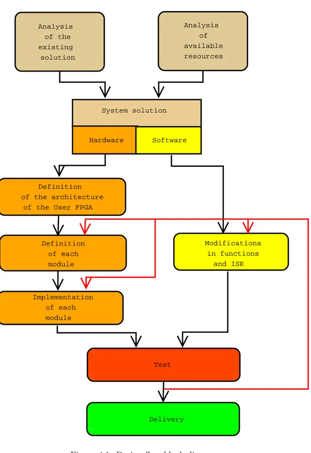
After the overview of the problem provided in the previous chapter, it’s time to describe the solution implemented with further details and the method used to design it.
4.1
The Design Flow
Let’s start with a description of the design flow. With the aid of the picture 5.1 I try to provide a clear picture of the whole work.
Analysis of the pre-existing solution The first step of the work is surely the analysis that was previously adopted for the audio port controller. This means a study of the audio port integrated circuit and of the pre-existing controller, provided as a Verilog described module, and all the software driver. This is the important to understand what could be still used (if anything) and what should be discarded.
Analysis of the available resources In parallel to this I studied the sys-tem in order to understand which where the resources available for the new design, in particular the architecture of the Test Chip and of the Development Board
4.1 The Design Flow
System Solution Thanks to both the previous steps I was able to propose a solution involving all the aspects of the final project. It was an high level solution where the main concerns was to partition the tasks to be implemented among hardware on the User FPGA and software running on the DSP. Once this division was clear I was able to work on both side almost independently.
Hardware design After this partition I designed the architecture of the User FPGA, that was previously blank. For this work I used a top-down approach, from the overall architecture down to the implementation of the single modules. A particular attention was paid to the design of one of these modules, the audio port controller, as described in the last section of the chapter 7.
Software design By knowing the definitions of the hardware in the User FPGA I was able to modify or to write from scratch the functions that were to be changed for the new controller.
Test of the integrated solution Particular attention was given to the test phase, that involved both hardware and software sometimes at the same time. Some tricks were used in the hardware design in order to make this phase easier. As described by the red lines in picture 5.1, a constant feedback was necessary on both hardware and software design.
In all this work I was aided by powerful hardware and software tools, that proved necessary for the overall success.
On the software side I used the DSP Development Environment CodeWar-rior by Metrowerks; with it I wrote the code (both C and assembly), down-loaded it on the Board and debugged it thanks to the On-Chip-Emulator.
On the hardware side I used the Quartus Environment by Altera, that allowed the development of HDL code to be mapped on the Stratix User FPGA. Thanks to this suite I was able to follow the typical design flow for Hardware FPGA programming that is:
4.1 The Design Flow Analysis of the existing solution Analysis of available resources System solution Hardware Software Definition of the architecture
of the User FPGA
Definition of each module Implementation of each module Test Modifications in functions and ISR Delivery
Figure 4.1: Design flow block diagram
4.2 Description of the solution
1. description of the hardware with HDL 2. functional simulation
3. fitting on the actual FPGA 4. timing simulation
5. programming of the FPGA
6. hardware testing of the system (aided by Signal TAP).
Until step five the design flow is quite straightforward; notwithstanding it’s worth noting that as the complexity of the system designed increased the ease of simulation decreased strongly. In my case it was mainly due to the presence of multiple communication channels (like buses) between my system on the FPGA and the outer world. Hence I preferred when possible to test the validity of my design directly on the FPGA; in this activity I was greatly supported by the Signal TAP controller that allows the recording and visualization of a number of signals in the design. Moreover testing this FPGA was done in great part by running some ad-hoc code on the DSP and verifying the expected behavior.
In some steps of the actual implementation I also had to make use of the oscilloscope to test some signals directly on the Printed Circuit Board.
After the introduction of the methods I used in this work I am going to speak about what I actually designed.
4.2
Description of the solution
As described in the previous section, one of the main steps in my design was the definition of a system solution, that provided a global picture. In this section I describe the results of this step, and the main ideas that lie underneath it.
The main problem, as already introduced, is to reduce the overhead due to the communication between the DSP and the audio port, by deploying the 37
4.2 Description of the solution
feature of the audio algorithms of being frame based. Hence some changes in the architecture or in the deployment of system resources are to be made. The first straightforward idea was the use of the Direct Memory Access bus, that connects the Test Chip to the User FPGA; as the name suggests, this bus allows a direct access to the memory without bothering the pro-cessor. Hence the samples from the Audio Port Integrated Circuit could be transferred to the internal memory via the User FPGA.
At this point, it would have been simple if the sample was to be written in the memory always at the same location. This is clearly wrong: the samples are to be stored in a vector one after the other. Moreover for the stereo signal there must be two vectors, and all this doubled for the outgoing samples.
So every time an audio value is sampled, there should be a transfer in the right place and the updating of some variables that describe the buffer. For this purpose some kind of controller is required that could access the internal memory and register of the audio port peripheral.
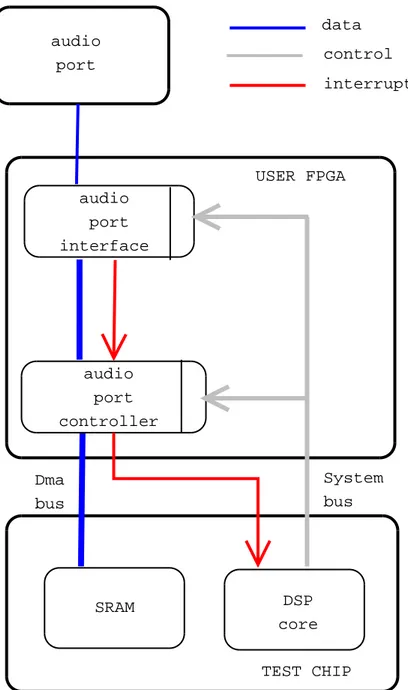
Moreover when the vector is full, the processor should be interrupted, to make it understand that a new frame of data is ready to be processed.
All these features come in the architecture described in picture 5.2; the main logical modules of this solution are the audio port peripheral and the audio port controller. These modules are both configured by the DSP pro-cessor via the Off-Chip System Bus; the peripheral is in charge of make the serial data coming from the audio port appear parallel, like a register. The controller on the other hand controls the transfer.
The whole system is timed by the interrupt sent at a frequency equal to the sampling rate by the audio port peripheral. This interrupt awakes the controller and enables the transfer. Depending on the configuration of the latter, when needed it sends another interrupt to the processor, that will eventually work on the data stored in the SRAM.
An alternative solution to this would be to implement a buffer in hard-ware, for example on the User FPGA. It would be necessary to store all the data in it and when it is full to send them in the internal SRAM via the
4.2 Description of the solution dsdf audio port audio port interface audio port controller SRAM DSP core USER FPGA TEST CHIP Dma bus System bus data control interrupt
Figure 4.2: System solution overview
4.2 Description of the solution
Off-Chip DMA Bus. This would not save any overhead, but the complexity would grow due to the presence of the buffer to be controlled. Another dis-advantage of this solution is that the variable would not be updated at every value, as it should be.
Part III
Third part
Chapter 5
The User FPGA System
Design and Implementation
The User FPGA is one of the two FPGAs on the Development Board, and it is where all the custom hardware I designed is hosted. This device, that is part of the Altera Stratix family, offers a huge amount of resources that are gates, memory and also specialized circuits. It has been added to the board to provide the user (i.e. the customer) with a further degree of freedom; in fact the user could custom the board by adding for example new controllers of peripherals, or a DMA controller. For this reason the board is usually delivered with the user FPGA blank, while all the basic functionalities and controllers are stored in the Control FPGA.
In this chapter I am going to describe the architecture of the digital system in this FPGA, and every single module that is part of it. There is a Control Register that contains configuration information, there are two bus interface, the audio port interface module and the audio port controller module.
To avoid confusion it’s necessary to specify the difference between audio port interface and audio port controller. The former is a digital block already existing that translate the serial communication of the audio port to a parallel register-like shape. The latter, that is the main part of my work, is a kind of wrapper of the audio port interface and controls the transfer of data between
5.1 The FPGA system architecture and flow of work
the registers into the internal memory. To the description of this module is dedicated the whole chapter 7.
So after some introductive details about the architecture and the design flow, all the other modules are described.
5.1
The FPGA system architecture and flow
of work
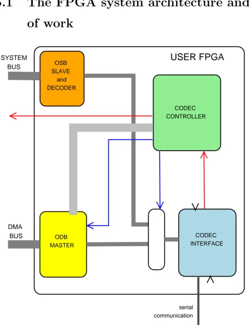
OSB SLAVE and DECODER ODB MASTER CODEC INTERFACE CODEC CONTROLLER SYSTEM BUS DMA BUS serial communicationUSER FPGA
Figure 5.1: Description of the FPGA system
5.1 The FPGA system architecture and flow of work
In this description of the architecture of the FPGA system I would start by considering which are the connections of this FPGA with the outer world. As you can see in the picture 6.1, there are two buses and the serial connection with audio port.
The first bus is the Chip System Bus (OSB), the second is the Off-Chip DMA Bus (ODB). The OSB is used to initialize both the audio port interface and the audio port controller, while the other is used just by the audio port controller to transfer data between the test chip memory and the audio port interface and to read and write data in the same memory.
It should be clear that since both of them are buses, they must have at least one master and at least one slave. Due to the configuration on the board the OSB require a slave that could understand the signal coming on the Test Chip while the ODB requires a master. Both this OSB slave and ODB have been implemented and could be seen in the picture 6.1.
Besides these buses there are three wires that are very important between User FPGA and TestChip: three interrupt wires. One of them is used to communicate an interrupt to the Test Chip from the audio port Controller.
On the audio port side there is the serial communication that is described with further details at page B.
From the picture 7.1 you can also see the connection of the audio port interface and controller, with the other modules. As a legend for that picture the wide gray lines are buses, the red lines are interrupt wires, and the blue ones are control signals.
5.1.1
The implementation flow
Besides the design flow I consider in this case interesting to dedicate some lines to the flow I had in the implementation of this hard module.
As at the beginning of my owrk the FPGA was really empty, the first thing that I had to design was the System Bus Slave; this is the only way to start having a look inside the FPGA: without this whichever other modules in the FPGA would have been stand alone, with no communication at all 44
5.2 The System Bus Slave and Decoder
with the TC, and with no possibility for me to understand whether they were working or not.
The second step was the porting of the Codec Interface from the Control FPGA to the User FPGA. This is the first layer of abstraction toward the Core; I made the Codec Interface registers accessible from the System Bus, and this allowed me to run a simple audio application with this new con-troller. The only difference with the original version was the FPGA in which it worked, in the original case the Control FPGA, and in my case the User FPGA.
Then I designed the Audio Port Controller, widely described in the next chapter.
Finally I designed the DMA bus master. Thanks to this the Test Chip memory could be accessed and data read and written from it. It is controlled by the Codec Controller, via a simple interface. This was the last hardware piece of my system, and it allowed to simulate and tune my whole system.
For all the duration of this implementation the size and definition of the User FPGA Control Register were continuously updated and reviewed, since new features were added during the work.
In the following sections I’ll describe the modules that compose the User FPGA, starting from the OSB Slave and Decoder.
5.2
The System Bus Slave and Decoder
The Off-Chip System Bus is a 32-bit AHB bus that extends the On-Chip System Bus. In the architecture of the board, there is a 256-Mbyte memory space reserved to the User FPGA, accessible via the Off-Chip System Bus, in the range between address 0xD0000000 and address 0xE0000000. This means that when in the software there is a read or write operation to a loca-tion in this range, the System Bus master on the Test Chip will interrogate the User FPGA.
Hence the function of the OSB Slave and Decoder is to make it possible
5.2 The System Bus Slave and Decoder
Name Width Address Access
FPGA Control Register 32 0xD0000000 RW
Controller Control Register 32 0xD0000004 RW Controller Address Register 32 0xD0000008 RW Controller Status Register 32 0xD000000C R Codec TX Left Channel Register 16 0xD0000010 RW Codec TX Right Channel Register 16 0xD0000014 RW Codec TX Command High Register 16 0xD0000018 RW Codec TX Command Low Register 16 0xD000001C RW Codec RX Left Channel Register 16 0xD0000020 R Codec RX Right Channel Register 16 0xD0000024 R Codec RX Command High Register 16 0xD0000028 R Codec RX Command Low Register 16 0xD000002C R Controller Program Memory 16 x 256 0xD0001000 RW
Table 5.1: Memory Space in the User FPGA
for the Test Chip to really access that memory area, complying the Standard AHB.
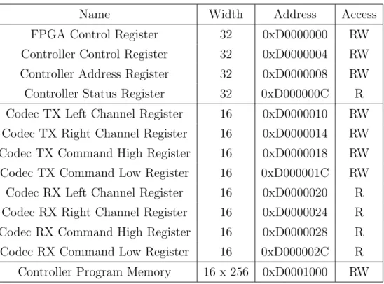
In my system I employed just part of the memory space available, and it is described in the table 6.1. There are mainly three different part of the memory:
32-bit registers used for different functions
audio port peripheral 16-bit registers used to store the values sampled by the audio port
512 byte memory to store the program of the controller
Given this memory space the role of this module is twofold; first it has to interpret the signals from the master and provide it with the correct signals according the standard. Then it has to make sure that the data on the bus
5.3 The User FPGA Control Register
are stored in the proper location (write case), or are loaded from the desired address (read case).
There is a couple of things I had to pay attention to in the design of this module; first of all I had to comply with the timing described in the AHB standard. As usual in this case a state machine was developed for the handshaking between master and slave.
A second important issue was dealing with the endianness of the system. In every elaboration system the memory stores data in two ways different ways, namely big endian and little endian; so in implementing a memory you have to take care of the endianness.
So in the case of 16-bit access in the User FPGA, according to the endi-anness value the meaningful bits would change their positions with respect to the 32 bits of the bus, and the bus slave should take this into account. Further details about this are in the appendix A, dedicated to AHB standard.
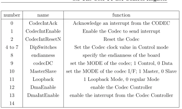
5.3
The User FPGA Control Register
The User FPGA Control Register is a 32 bit register at the address 0xD0000000, that is the first available on the FPGA; this register is accessed by the core to control the behavior of the FPGA, in particular of the audio port interface and of the audio port controller.
Table 6.2 contains a summary of all the values in that register. To under-stand the architecture and the behavior of the FPGA is necessary to focus on many of these bits, one by one.
DmaEnable This bit enables the Controller to work. When it is zero the Audio Port Interface is connected directly to the System Bus Slave, and its interrupt request goes directly to the core. Instead, when this bit is set, the Controller stands amidst the Codec Interface and the DMA Bus Master. The Codec registers in this case are accessible from the OSB in read only mode. This is the typical running mode, where
5.3 The User FPGA Control Register
number name function
0 CodecIntAck Acknowledge an interrupt from the CODEC 1 CodecIntEnable Enable the Codec to send interrupt
2 CodecIntResetN Reset the Codec
4 to 7 DipSwitches Set the Codec clock value in Control mode 8 endianness specify the endianness of the board 9 codecDC set the MODE of the codec; 1 Control, 0 Data 10 MasterSlave set the MODE of the codec I/F; 1 Master, 0 Slave 11 Loopback 1 Loopback Mode, 0 regular Mode
12 DmaEnable enable the Codec Controller
13 DmaIntEnable enable the interrupt from the Codec Controller 14
Table 5.2: Control Register bit table
the Audio Port Controller is awake and generate, when it is necessary, the interrupt request to the core.
Loopback This makes it possible to test the Interface. In this configura-tion the Codec Rx wire of the serial communicaconfigura-tion, is shorted to the
Codec Tx ; for the Interface to work properly you expect the Codec RX
registers to reply exactly what you write in the Codec TX registers1. endianness This bit indicates the endianness of the board. Please consider
that endianness doesn’t affect the 32-bit operations; thanks to this it is possible for the Core to communicate this information to the FPGA by making a 32-bit write operation in the Control Register. This con-figuration must be the first done by the software at power on ; then this bit is used by the two bus controllers to work in the correct way. codecDC This bit is one of the Audio Port Serial Interface. It is changed
by the ISR during its control section (see page 73), to change the mode of the codec from Config to data.
1For the function of these registers see the Audio Port Interface section
5.4 AHB Off-Chip DMA Bus Master
CodecIntEnable Enable the Interface to send interrupt request; depending on the DmaEnable bit, the IRQ could reach either the DSP or the Coded Controller;
DmaIntEnable Enable the Codec Controller to send an interrupt request to the DSP.
5.4
AHB Off-Chip DMA Bus Master
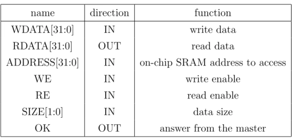
Another important module in the User FPGA system is the Off-Chip DMA Bus Master. Its role is to provide the right signal to the bus wires always complying with the AHB-standard. Moreover it has to provide the Controller with a simple interface that lets the Controller easily use the DMA bus.
The signals of the interface I designed are described in the table 6.3; besides the data and address wires it is worth speaking about the control signals. The audio port controller controls write enable, read enable and
size; when it wants to perform an operation it raises one among re and we
and put the right value on size. The Master, if ready to accept, will drop the ok signal, meaning that it became busy; the controller knows that the operation is finished when ok is raised again, and if it is a read operation it will read the proper value on the RDATA signal.
Due to possible problems in the communication I also implemented a time-out mechanism that forces each operation to end after 20 cycles, if not already finished.
5.5
The Audio Port Interface
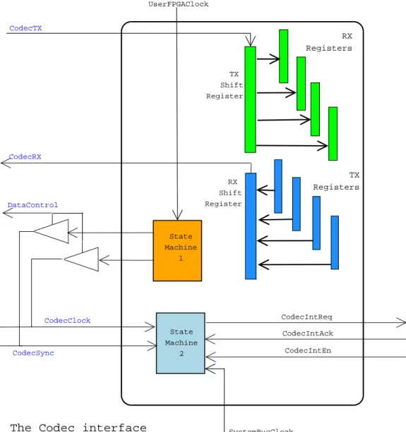
The last block to describe before the audio port controller is the audio port interface, the digital block that stands between the audio port IC and the DSP, to make the two work together. As previously said it is a pre-existing module, and this section I am just going to describe it. In the picture 6.2 there is an overview of it. You can see the five signals that compose the 49
5.5 The Audio Port Interface
name direction function
WDATA[31:0] IN write data
RDATA[31:0] OUT read data
ADDRESS[31:0] IN on-chip SRAM address to access
WE IN write enable
RE IN read enable
SIZE[1:0] IN data size
OK OUT answer from the master
Table 5.3: DMA bus signals
serial communication to the integrated circuit; they are CodecClock,
Codec-Sync, CodecTx, CodecRx andControlData and they are connected to the
corresponding pins of the integrated circuit.
The data wires are connected to a 64-bit shift register each; this is then connected to a group of four 16-bit registers. This simple systems makes the translation from serial to parallel communication. Both the dma bus and the system bus can access those registers, with the mode described in table 6.5. The CodecClock and CodecSync are bidirectional pins, that could be driven by the interface. This happens during the Audio Port configuration phase2: the State Machine 1 generates a a clock and a sync signal for the Audio Port, from the UserFPGAClock. The ControlData pin, set to zero, let the signals generated to drive the actual wires of the interface through the tristate buffer.
As soon as the data mode is entered (and the ControlData is set), the clock and the sync will be provided by the Audio Port, at the frequency configured. In both mode the State Machine 2 is fed with sync and clock, in order to generate an interrupt to the core, or to the controller.
The interrupt is clearly at the same frequency of the sync signal, that is basically the sampling frequency. The interrupt means that there are data ready for the application in the RX registers, and that the TX registers are
2see 8.3 for explanation
5.6 The issue of synchronous design
empty and they could be filled with new data.
Register name function access mode system bus address
LchTxReg Left Channel Transmit Register write-only 0xD0000010 RchTxReg Right Channel Transmit Register write-only 0xD0000014 CmhTxReg Command High Transmit Register write-only 0xD0000018 CmlTxReg Command Low Transmit Register write-only 0xD000001C LchRxReg Left Channel Receive Register read-only 0xD0000020 RchRxReg Right Channel Receive Register read-only 0xD0000024 CmhRxReg Command High Receive Register read-only 0xD0000028 CmlRxReg Command High Receive Register read-only 0xD000002C Codec register table
5.6
The issue of synchronous design
The whole system is basically composed by the Test Chip, the User FPGA and the audio port IC. During the ordinary activity the audio port is con-figured to be the master of the serial communication, so this adds an asyn-chronous component to the system; since I am going to use the Codec I/F as it is, the problem should have been already faced and I am not going to deal with it. I would rather focus on the communication between the Test Chip and the FPGA; it is done by two buses and the clock is provided in both cases by the Clock Generator in Test Chip, that is software programmable. The System Bus clock is the one used in the DMA system. The default configuration is 45 MHz for both, but no software control is given on their phases; it could have been an important issue if there was a phase delay.
Luckily the results of measurement gave a positive answer, meaning that the two signals could be considered really synchronous, letting me consider all this part a complete single clock part.
5.6 The issue of synchronous design CodecTX CodecRX CodecSync CodecClock UserFPGAClock SystemBusClock CodecIntReq DataControl CodecIntAck CodecIntEn RX Registers TX Registers TX Shift Register RX Shift Register
The Codec interface
State Machine 1 State Machine 2
Figure 5.2: Audio Port Interface
Chapter 6
The Audio Port Controller
This chapter deals with the audio port1 controller, its design and its archi-tecture. To implement this module among the possible choices I decided to design a kind of micro-controller; the reason for this choice and some details on its features are in the first section. In the remainder of this chapter there is the description of all the modules that compose the micro-controller.
6.1
The Audio Port Controller Design Flow
In this first section I am going to explain the choice in the implementation of this module. It all starts with the tasks it has to accomplish; it is described in the section 8.4, but at this stage it’s enough to say that it is quite complex and not a priori easily and exactly definable.
Since that complexity looked to be very high I decided to use a pro-grammable module, a kind of CPU with its program memory. It is true that during the ordinary life of the final product there is no need of pro-grammability, but I thought that this would have been a great advantage in the development of this module. This causes a little increase in the amount of resources taken for the design, but since the User FPGA was really huge, I estimated that this wouldn’t have been an issue. As you can see in the