UNIVERSITÀ DEGLI STUDI DI CATANIA
Ph.D. in Materials Science and Nanotechnology XXXI Cycle
Ph.D. Thesis
Synthesis of hybrid metalorganic/inorganic
systems and doped halide thin films for
photovoltaics
Ph.D. Student:
ANNA LUCIA PELLEGRINO
Supervisor: Coordinator:
Prof. Graziella Malandrino Prof. Maria Grazia Grimaldi
2016-2018
1
Contents
Introduction 4
1. Photovoltaic Materials 9
1.1 Photovoltaic technology: state of art 9
1.2 Lanthanide doped fluoride thin films 11
1.3 Hybrid organic/inorganic systems 19
1.4 Inorganic halide perovskites 21
References 24
2. MOCVD fabrication of Ln3+ doped fluoride thin films 32
2.1 Introduction 33
2.2 Ln3+ doped CaF2 thin films: MOCVD fabrication and their
up-conversion properties
34
2.2.1 Experimental Section 35
2.2.2 Results and discussion 36
2.2.3 Luminescent proprieties 43
2.3 NaYF4 thin film: MOCVD growth of cubic and hexagonal phases 46
2.3.1 Experimental Section 46
2.3.2 Results and discussion 47
2.4 KYF4 thin films: MOCVD synthesis through a new β-dichetonate
heterobimetallic potassium- yttrium precursor
52
2.4.1 Experimental Section 52
2.4.2 Synthesis and characterization of a novel
KY(hfa)4•tetraglyme
53
2.4.3 KYF4 MOCVD synthesis: results and discussion 56
2
References 60
3. Sol-gel approach to the fabrication of Ln3+ doped fluoride thin films 63
3.1 Introduction 63
3.2 Ln3+ doped β-NaYF4 thin films: Sol-gel fabrications and their
luminescent properties
65
3.2.1 Experimental Section 66
3.2.2 Synthesis and characterization of a novel Na(hfa)•tetraglyme 67
3.2.3 Optimization of the sol-gel process for the formation of
β-NaYF4 phase films
71
3.2.4 Co-doped Yb3+/Er3+ and Yb3+/Tm3+ β-NaYF4 phase thin films 77
3.2.5 Upconversion properties and luminescence lifetimes of the
co-doped β-NaYF4:Yb3+, Er3+ and Yb3+, Tm3+ films
80
3.3 Ln3+ doped β-NaGdF4 thin films 85
3.3.1 Sol- gel process for the formation of β-NaGdF4:Eu3+ phase
films
86
3.3.2 β-NaGdF4:Eu3+ thin films: analysis of phase stability vs
annealing temperature
87
3.4 Ln3+ doped YOFthin films 89
3.4.1 Sol- gel process for the formation of YOF thin films 90
3.4.2 Structural, morphological and compositional characterization
of Ln3+ doped YOF thin films
91
3.5 Conclusion 94
References 95
4. Combined MOCVD/MLD approach for hybrid metalorganic-inorganic systems of NiO thin films with a luminescent europium complex monolayer
98
3
4.2 Experimental Section 100
4.2.1 Precursors synthesis 100
4.2.2 MOCVD/MLD synthetic approach 101
4.3 Results and discussion 103
4.3.1 Monolayer characterization 104
4.3.2 Luminescent properties of the monolayer 109
4.4 Conclusion 111
References 111
5. Synthesis of inorganic perovskite CsPbBr3: study of phase stability 113
5.1 Introduction 113
5.2 Experimental section 115
5.3 Results and discussion 115
5.4 Conclusion 122
References 123
Conclusions 124
4
Introduction
The current energetic scenario has led the development of systems in which the renewable sources are economically competitive with "traditional" sources, reducing production costs and increasing conversion efficiencies. In this field, the photovoltaic approach is one of the most promising technologies, which allow to exploit the advantages of the solar source and to cover the electricity demand. Nowadays, several research fields are focused on the study of improving the performance of commercial photovoltaic modules through a more efficient exploitation of the solar spectrum. In this context, the aim of the present study is the development of new materials of interest for the photovoltaic (PV) technologies.
The most mature technology to date is based on silicon cells. The conversion efficiency of these solar cells varies from 6% for the amorphous Si up to 24.7% of prototypes obtained in the laboratory.
One possible way to increase the conversion efficiency of silicon solar cells is to shift the incident sunlight spectrum, converting photons poorly exploited by silicon into more effective photons. A better utilization of the solar spectrum can be obtained by converting photons with wavelengths higher or lower compared to the solar cell efficiency range into optimal wavelength range. The three conversion processes of interest are: up-conversion (UC), down-conversion (DC) and energy down-shifting. The materials studied as energy converters, consist of thin film layers integrated in the PV panel and made of two components: a host material and an active luminescent species that allows the conversion. In literature, the materials used as host matrices are polymeric composite layers, inorganic crystalline materials and various kind of glasses. The host material exhibits high transmission in the spectral region where the cell response is high and at the same time it guarantees an optimal environment for the luminescent component. The luminescent species used
5
in these layers represent the active centers of the energy conversion process. In particular, quantum dots and organic dyes are the most used species applied in PV devices together with ions and rare earth complexes due to their luminescent properties, which cover the ultraviolet (UV), visible and near infrared (NIR) range. In the present thesis, the energy conversion systems made of lanthanide doped binary and multicomponent fluorides (CaF2, NaYF4, NaGdF4, KYF4 and YOF) have
been synthetized and deeply studied for their potential integration in silicon solar cells, due to the energy conversion processes of Ln ions. Starting from the β-diketonate metal complexes, two different synthetic approaches have been tested: metalorganic chemical vapor deposition (MOCVD) and sol-gel method.
Together with the traditional and well-known silicon PV technology, a new class of PV materials is subject of interest in the last years. In particular, the third generation solar cells represent the new technology with higher efficiency, based on inorganic multi-junction technology, new hybrid and inorganic semiconductor materials such as perovskite ABX3 (A= [(CH3)NH3]+ and Cs+ ; B=Pb2+,Sn2+ and X= Cl
-,Br-,I-) and organic dye-sensitized solar cells (DSSC). In particular, the perovskite
solar cells (PSCs) attract worldwide attention with always higher record in the power conversion efficiency and with the additional possibility of combining the advantages of mechanical, electrical, magnetic, optical, and transport properties. This recent generation of solar cell technology is of interest for industrial applications because of the advantages of low-cost, low-temperature processing, flexible substrates, and large-area fabrication processes.
In the present thesis, hybrid metalorganic/inorganic systems Eu-complex/NiO have been synthesized for the DSSC technology and for the potential improvement of the PV material with new functionalities, that combine the semiconductor behavior of the inorganic part to the luminescent properties of the metalorganic component. Nickel oxide has been chosen as the inorganic component of the hybrid system due to its multifunctional properties such as electrochromic and antiferromagnetic properties, high dielectric constant, UV optical transparency and p-type
6
semiconducting behavior. Lanthanide complexes have been chosen due to their luminescent properties, in particular Eu complexes have attracted growing interest because Eu is one of the most efficient downshifter.
In addition, all-inorganic halide perovskite CsPbBr3 has been synthetized through a
precipitation method using Cs and Pb metal complexes and Br2 as precipitating
agent. The all-inorganic halide perovskite CsPbBr3 has a semiconductor behavior,
with an energy band gap useful in the PV application. Compared to the well-known hybrid perovskite, such as MAPbI3 (MA: methyl ammonium), the CsPbBr3 has the
advantages to not have any labile or expensive organic components and shows remarkable stability under humidity conditions and extreme temperatures.
In summary, the present PhD thesis is organized in the following chapters and a schematic table (Table 1) is reported to summarize the materials object of the present study:
• Chapter 1 emphasizes the aim of the present study and the main photovoltaic technologies of importance in the recent years. An outlook regarding the materials of interest in the photovoltaic technology field has been described, together with the new strategies to increase the photovoltaic efficiency in solar cells.
• Chapter 2 focuses on the synthesis of CaF2 films doped with Yb3+,Er3+ or
Yb3+,Tm3+ through MOCVD route using a molten mixture consisting of the
Ca(hfa)2•diglyme•H2O and the suitable Ln(hfa)3•diglyme precursors in an
appropriate stoichiometric ratio. In addition, MOCVD approach is applied to the fabrication of the multicomponent fluoride β-NaYF4 and KYF4 thin films as
well. The fluorinated “third-generation” bimetallic precursors, NaY(hfa)4tetraglyme, synthetized in a previous work, and the novel
7
achieved through an accurate optimization of the operative parameters, such as deposition temperature, vaporization temperature of the precursors and choice of the substrates.
• Chapter 3 concentrates on an innovative sol-gel process to produce Ln3+doped
β-NaREF4 thin films (Ln: Eu3+, Yb3+, Tm3+, Er3+ and RE: Gd, Y), using a mixture
of a novel β-diketonate sodium precursor Na(hfa)•tetraglyme and a rare earth precursors RE(hfa)3•diglyme (RE=Y, Gd, Eu, Yb, Tm, Er). Furthermore, the sol
gel method has been successful applied for the synthesis of Ln3+ doped r-YOF
thin films as well. These final goals have been achieved through an accurate optimization of the operative parameters, such as effects of molar ratio of the precursors, aging time of sol and annealing treatment. Their structural and morphological properties are studied in details.
• Chapter 4 highlights a novel full vapor phase approach applied for the synthesis of hybrid metalorganic/inorganic systems. The process is based on the sequential steps of MOCVD of the inorganic NiO thin films and molecular layer deposition (MLD) to link on the activated surface in a covalent way a luminescent Eu(III) complex. An accurate X-ray photoelectron characterization confirmed the optimal parameter condition of the activation step and of the covalent anchoring of the Eu complex on NiO films.
• Chapter 5 reports the successful fabrication of the all-inorganic halide perovskite CsPbBr3 using the β-diketonate complexes [Pb(hfa)2diglyme]2,
Cs(hfa) through a precipitation method in ethanol and water solution with Br2.
The control of temperature and aging time for the formation of the pure phase CsPbBr3 crystals has been deeply investigated.
8 PHOTOVOLTAIC MATERIALS OF INTEREST
PV TECHNOLOGY MATERIAL PRECURSORS METHOD CHAPTER
Energy conversion systems for silicon solar cells
Lanthanide doped binary and multi-component fluorides CaF2: Yb3+, Er3+ / Yb3+, Tm3+ Ca(hfa)2•diglyme•H2O Ln(hfa)3•diglyme MOCVD 2.2
β-NaYF4 NaY(hfa)4tetraglyme MOCVD 2.3 β-NaYF4:
Yb3+, Er3+ / Yb3+, Tm3+
Na(hfa)•tetraglyme RE(hfa)3•diglyme
(RE=Y, Yb, Tm, Er)
Sol-gel 3.2
NaGdF4: Eu3+ Na(hfa)•tetraglyme
RE(hfa)3•diglyme
(RE=Gd, Eu)
Sol-gel 3.3
KYF4 KY(hfa)4tetraglyme MOCVD 2.4 YOF: Yb3+, Er3+ / Yb3+, Tm3+ Y(hfa)3•diglyme Ln(hfa)3•diglyme (Ln: Yb, Tm, Er) Sol-gel 3.4 Dye-sensitized
solar cells metalorganic/ Hybrid inorganic
systems
Eu-complex/NiO Eu(hfa)3phen MLD 4
Perovskite solar
cells Inorganic halide perovskite
CsPbBr3 [Pb(hfa)2diglyme]2
Cs(hfa)
precipitation
method 5
9
CHAPTER 1
Photovoltaic Materials
1.1 Photovoltaic technology: state of art
A photovoltaic system has the property of absorbing photons and generating electrons for electrical conduction. In recent years, the evolution of solar cells, due to technological and economic progress, has developed through the growing of three different photovoltaic generations.
The first generation solar cells are relatively expensive to produce, and have a low efficiency in relation to production costs. The first generation includes single-junction devices made of crystalline silicon (mono and multi-crystalline), which converts directly solar radiation into electrical energy. This kind of cells has two doped silicon layers in order to obtain a p-n junction. This technology achieves a conversion efficiency around 25% for based c-Si cells and about 20% for mc-Si cells.
The second generation is characterized by lower yield than the previous ones but has lower production cost. This technology is based on the production of Si thin film cells, with thickness between 1 and 10μm, which yields flexibility properties. However, this kind of cell has slightly lower efficiency with respect to the previous generation. Another aspect of this second generation technology is the use of new materials such as amorphous silicon (a-Si), and composite materials such as indium-copper-gallium diselenide (CuIn(Ga)Se2 or CIGS) or cadmium telluride (CdTe).
The third generation solar cells represents the new technology and has the higher efficiency, and can be divided into two categories:
10
➢ inorganic cells, which use semiconductor materials such as the previous ones and the hybrid or inorganic perovskites ABX3 (A= [(CH3)NH3]+ and Cs+ ;
B=Pb2+,Sn2+ and X= Cl-,Br-,I-);
➢ organic cells, which use polymers or organic dyes.
The inorganic third generation cells are based on multi-junction technology, using up to four overlapping cells of semiconducting materials in tandem configuration, and currently show the highest efficiency values. Very recently the new organic−inorganic hybrid halide perovskite materials have become promising candidates for efficient inorganic third generation solar cells.
The organic third generation cells, known as Dye Sensitized solar cells (DSSC), have the advantages of the organic materials in terms of very low costs of material and production, due to the easy processing through deposition on transparent, flexible and large area substrates. However, currently the highest efficiency for this kind of cells is around 11% and they present limits regarding their duration.
In this scenario, an interesting perspective is the possibility to increase the efficiency of a photovoltaic cell, independently on its nature, by collecting the radiation energy outside the absorption range of the photoactive material by shifting its energy to a more suitable optical region through down-conversion (DC) or up-conversion (UC) processes. Down-conversion is the process by which one high energy photon, which is inefficiently absorbed by the photovoltaic cell due to thermalisation losses, is converted into two or more lower energy photons. The DC layer is placed in front of the cell and the generated photons all have sufficient energy to be absorbed by the photovoltaic cell, with negligible thermalisation loss. Up-conversion is the process by which two or more low energy (long wavelength) photons, which are transmitted by the photovoltaic cell, are converted into one high energy photon. Thus an UC layer placed behind a PV device can harvest the solar radiation energy outside the PV absorption range and convert it into useful photons with energy inside the band of the semiconductor used in the PV device.
11
The aim of the present study is the development of new materials of interest for the photovoltaic technologies. Lanthanide doped fluoride materials CaF2, NaYF4,
NaGdF4, KYF4 and YOF have been synthetized and deeply studied for the
possibilities of increasing the efficiency yield in the a-Si and mc-Si cells, due to the energy conversion processes of Ln ions. These systems in fact, could enhance the photovoltaic efficiency and could be easily integrated in the PV panel.
The hybrid metalorganic/inorganic systems Eu-complex/NiO has been synthetized for the DSSC technology and for the potential improvement of the PV material with new functionalities, that combine the semiconductor behavior of the inorganic component to the properties of the organic component.
Finally, the inorganic halide perovskite CsPbBr3 has been synthetized through a
precipitation method. The all-inorganic halide perovskite CsPbBr3 shows a
semiconductor behavior, with an energy band gap useful in the PV application of the new third generation perovskite solar cells.
1.2 Lanthanide doped fluoride thin films
In the last years, much attention has been focused on luminescent rare-earth (RE)-doped materials, for their large variety of modern technological applications, ranging from phosphors [1-2] to solar cells [3], from flat-panel displays [4], to solid state lasers [5], from photocatalysis [6], to diagnostic tools in nanobiomedicine [7]. Very recently lanthanide doped materials have been proven also interesting in form of homogenous films for microelectronics applications, to map the temperature distribution inside integrated circuits in non-contact mode and with high spatial resolution, using the different luminescent emission of the lanthanides at different temperatures [8]. Lanthanide doped fluoride materials have been deeply studied for their unique properties in the ultraviolet, visible and IR range. In fact, a proper combination of doping ions and host material produces an efficient energy conversion mechanism upon light irradiation [9]. In particular, ternary fluoride
12
compounds, like the NaYF4, NaGdF4 and KYF4 and binary fluoride MF2 (M: Ca, Sr),
have been thoroughly studied as host materials for doping luminescent Ln3+ (Ln =
lanthanide) ions to achieve the desirable down-conversion (DC) or up-conversion (UC) processes [10].
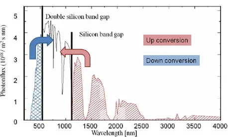
In particular, UC is a process whereby two or more low energy photons are converted into higher energy photons, and DC, on the contrary, is a process in which higher photons are converted into more photons with lower energy. These forms of spectral conversion have been considered as a provision in the area of photovoltaics (PV) [11], to reduce the intrinsic losses associated with the transmission of sub-bandgap photons (fig. 1) [12]. In fact, as shown in fig. 1, down-conversion shifts photons from a high-energy band (blue) to the maximum absorption band of silicon (white); up-conversion shifts photons from a low-energy band (red) to the maximum absorption band of silicon [13, 14].
Fig. 1 Solar spectrum showing the band gap and twice the band gap of silicon and the UC and DC
shifting [13].
Several mechanisms, originated from transitions within the 4f configuration of Ln-doped nanomaterials, are known to guide the energy conversion emissions.
13
The DC mechanism is the process where one photon with a high energy is cut to obtain two photons with a lower energy. Cutting of one high energy photon to obtain two lower energy photons on a single lanthanide ion is known as cascade emission (fig. 2a) and has been known to occur for Pr3+ [15], Tm3+ [16] and Gd3+ [17].
Down-conversion with pairs of lanthanide ions can occur through various mechanism, shown in fig. 2b, c, d. For all three mechanisms ion I is first excited into a high energy level. Figure 2b shows the emission of two photons from ion pairs via cross-relaxation between ions I and II followed by energy transfer from ion I to ion II and emission from ion II. Figures 2c, d show mechanisms involving on energy transfer step between ions I and II, and emission of a photon by both ions.
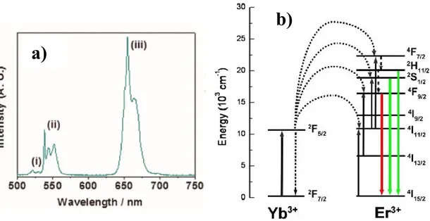
UC is the process where two photons with a smaller energy are added up to obtain one photon with a high energy. Figure 3 gives an overview of the possible up-conversion mechanisms. The most efficient process is the mechanism called Energy Transfer Up-conversion (ETU), in which two ions of type I absorb a photon and give the energy to ion II in two steps via an intermediate level on ion I (fig. 3a). This can also be described as ground state absorption (GSA) followed by an energy transfer step, known as GSA/ETU. Up-conversion on a single ion (fig. 3b) can occur when the ion is already in the excited state and a second photon is absorbed. This mechanism is known as GSA followed by excited state absorption (ESA), and it is the second most efficient mechanism. For UC with these two mechanisms it is necessary that the second excitation step of ion I is faster than both the radiative and non-radiative decay from the intermediate level. Both of these mechanisms involve real intermediate energy levels. The other four mechanisms shown in fig. 3c-f involve one or more virtual energy levels, and therefore have lower efficiencies.
14
Fig. 2 Schematic representation of several different down conversion mechanisms. Solid vertical
arrows indicate radiative transitions. Arrows connecting different ions and dashed arrows indicate energy transfer between ions.
Fig. 3 Energy level schemes for several different 2-photon up-conversion mechanisms. Solid vertical
arrows indicate radiative transitions. Arrows connecting different ions and dashed arrows indicate energy transfer between ions [18].
The energy transfer up-conversion (ETU) is the most efficient processes for Yb3+/Ln3+
co-doped fluoride. Trivalent lanthanide ions, like Er3+, Tm3+, Nd3+ or Ho3+, are the
most common activator ions for the ETU process due to their peculiar energy level schemes and narrow emission spectral lines, and the Yb3+ ion is the useful sensitizer
with a large absorption in the IR range [19].
In regard to the host material, fluorescent fluoride hosts, in comparison with conventional oxide luminescent systems, are attractive because of their high optical
15
transparency from UV through IR, high chemical stability, high refractive index and low phonon energy, which enables the radiative transitions of lanthanide ions to occur with high efficiency [20].
CaF2
Calcium fluoride has the typical fluorite structure, following the name (fluorite) of the mineral form of CaF2, which is a simple cubic arrangement of anions with 50%
cubic sites filled with Ca2+ (fig. 4). Thus, in this structure, calcium is eight coordinated
by fluoride ions, a coordination environment suitable for the lanthanide ions, being eight the most common coordination number for lanthanides [21].
Fig. 4 Fluorite structure.
Most of the above-mentioned applications require the calcium fluoride material in the form of thin films. Several studies are available on the deposition of CaF2 thin
films using physical vapor deposition techniques, such as sputtering [22], electron beam evaporation [23], pulsed laser deposition [24], and molecular beam epitaxy [25]. Calcium fluoride films have also been deposited through sol–gel chemical routes using spin coating or dip coating [26]. Among the chemical vapor deposition approaches, atomic layer deposition has been applied to the deposition of CaF2 films
[27]. Nevertheless, even though various deposition methods have been applied to the
Ca2+
-16
fabrication of CaF2 films, a more versatile, easily scalable, fast, and industrially
appealing approach is highly desirable [28].
MOCVD has been also applied to the deposition of the fluorite films; nevertheless, most of these reports used a fluorine-free calcium source, thus a second precursor is needed as the fluorine source. The first report on the deposition of CaF2 with
MOCVD dates back to 1989 when the bis(pentamethyl-cyclopentadienyl)calcium was applied as calcium source together with SiF4 or NF3 as fluorine source [29]. More
recently, fluorine free β-diketonate has been applied as calcium source combined with the use of ammonium hydrogen fluoride as the fluorine source [30]. A few reports are described in the application of fluorinated precursors to the fabrication of thin films where polyether adducts of the Ca bis-hexafluoroacetylacetonate have been applied, namely, the Ca(hfa)2•tetraglyme [31] and the Ca(hfa)2•diglyme•H2O
[32].
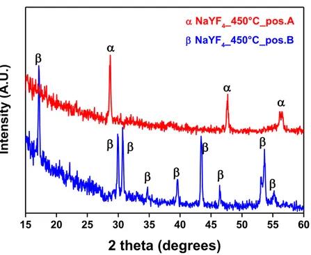
NaREF4
The crystal structure of NaREF4 exhibits two polymorphic forms, namely, cubic (α)
and hexagonal (β) phases (fig. 5). The cubic α-NaYF4 structure is isostructural to
fluorite. The hexagonal β-NaYF4 structure, of interest in this work due to its efficient
host behavior, presents instead a distribution of cations in the lattice controversial [33]. The X-ray diffraction patterns of this phase do not fit well the crystalline structure, reported for the known NaNdF4 [33]. The Na:M ratio (M = Y, Nd, Er, Tm,
Yb) of the hexagonal phase deviates from the expected 1: 1 value, and it depends on the M species and the preparation temperature. Therefore, it is proposed that the β-NaYF4 phase is isostructural with chloride phases of Na3xM2-xCl6 stoichiometry (M =
La - Sm). This structure, characteristic of gagarinite, contains only one M3+ site which
is occupied by Na+ and M3+ ions in non-stoichiometric ratios with the final formula
Na3xM2-xF6 (x = 0.45 - 0,5). Therefore, the hexagonal phase is known as Na1.5Y1.5F6 as
17
Fig. 5 Cubic (α) and hexagonal (β) phases of NaYF4 crystal structure.
Several investigations have shown that the hexagonal phase is a much better host lattice than the cubic one for energy conversion applications [35]. Therefore, an accurate control for the selective and reproducible fabrication of the β-NaREF4:Ln3+
single phase is a stringent requirement for high energy conversion performance. At the same time, a controlled dispersion of the luminescent Ln species in the host matrices plays a key role, since the local environment around the luminescent ions strongly affects the emission performances of the materials [36]. Until now, several methods have been employed to obtain Ln doped β-NaREF4 nanocrystals, including
co-precipitation [37], solvothermal [38], thermal evaporation [39], and molten salt method [40]. Recently, few studies have been reported on the fabrication of complex core-shell architectures and their up-conversion performances [41]. Only a few reports are available, to the best of our knowledge, about NaYF4 thin films and the
study of their energy conversion properties [42].
YOF
Oxyfluorides' crystal structures (YOF and LaOF) exhibit three different crystal lattices: cubic, rhombohedral and tetragonal, which is usually nonstoichiometric (REOnF3-2, 0.7<n<1) [43]. The rhombohedral structure (r-YOF) is the stable one, and it
18
is strictly stoichiometric (n=1) (fig. 6). The cubic YOF structure occurs as the result of the phase transition from the rhombohedral phase at temperature of 560–570°C [44]. Tetragonal crystal form has been observed usually in nonstoichiometric compounds, but additional studies have shown that these materials are more complex than it was previously assumed; for example compound with general formula REnOn-1Fn+2, 5 ≤ n ≤
9 such as Y5O4F7, Y6O5F8 and Y7O6F9, which crystallize in an ortorhombohedral form
[45-47].
Fig. 6 Rhombohedral structure of YOF.
Lanthanide doped oxyfluorides have been a matter of interest for their utilization in many important technologies, such as lasers, electronics, therapeutics, displays, solar cells, catalysis, medicine [48–51]. In addition, there is a growing interest for their use as bio-markers or nano-sensors [52]. These materials are promising hosts for preparation of phosphors due to their attractive chemical and physical properties which may be classified as in between characteristics of fluorides and oxides [44,53]. Alike fluorides, oxyfluorides have low phonon energy and high ionicity which leads to the efficient luminescence, while, on the other hand, these compounds have great
19
chemical and thermal stabilities which resemble properties of oxides [48,49]. In addition, oxyfluoride nanomaterials are biocompatible and nearly nontoxic to live cells so they can be used for biomedical applications [51,54].
To prepare oxyfluorides, several methods can be employed: thermolysis method, fluorolytic sol-gel, hydrothermal method, co-precipitation method, solid state synthesis [50,55]. To our knowledge, only one study has been reported on the synthesis of YOF thin film [56].
1.3 Hybrid organic/inorganic systems
Nowadays the organic-inorganic hybrid systems made of inorganic thin film with surfaces functionalized by covalent attachment of organic molecules have attracted great attention because of their potential applications in several fields of material science [57–58] such as sensors [59], dye sensitized solar cells (DSSCs) [60], optoelectronic devices [61], and heterogeneous catalysis [62]. In these systems, transition metal oxides thin films are the most promising inorganic materials [63], due to their wide spectrum of magnetic, electrical, and optical properties [64]. In this context the anchoring of organic luminescent complexes on the oxide surface [65] leads to a new multifunctional materials with a wide range of modular properties [66], and therefore a broad range of applications [67].
Among transition metal oxides, nickel oxide has been chosen as the inorganic component of the hybrid system due to its multifunctional properties such as high dielectric constant, low resistivity and UV optical transparency [68]. Nickel oxide has also electrochromic and antiferromagnetic properties and a p-type semiconducting behavior. For these wide range of properties NiO has been studied as material for organic light-emitting diodes (OLED) [69], tandem photocathodes for dye-sensitized solar cells (DSSC) [70], smart windows [71], Schottky devices [72], and chemical sensors [73].
20
In regard to the synthesis approach for NiO thin films many methods have been reported in the literature such as thermal evaporation [74], pulsed-laser-deposition (PLD) [75], reactive magnetron sputtering [76], metal organic chemical vapor deposition (MOCVD) [77], intermittent spray pyrolysis [78] and sol–gel deposition [79]. Among these strategies, MOCVD has been chosen in this work as synthetic method because of its reliable and reproducible production in large scale and highly uniformity in thickness and composition.
In relation with the nature of inorganic film, the most common functional organic moieties chosen for the hybrid approach are the molecules having silane [80], thiol [81], and carboxylic functionalities [82] as anchoring groups. As alternatives, also organophosphorus compounds were tested as linkers for the functionalization of metal oxide surfaces [83]. Among these wide families of functional molecules the attention has been devoted to luminescent lanthanide complexes due to the exceptional photophysical properties such as high quantum yields, long excited-state lifetimes, large Stokes shifts and sharp emission profiles related to f–f electronic transitions. Eu(III) complexes have attracted growing interest as efficient downshifter, probe to sense the chemical environment and for its luminescent behavior.
For a variety of applications, the possibility of a fast, high efficient and reproducible assembly method of molecules into nanostructured solid substrates is of a great importance. Up to date, most of the synthetic approach to prepare hybrid systems have applied solution routes such as sol-gel procedure [84], Langmuir-Blodgett techniques, self-assembly procedures and gas-phase route such as atomic layer deposition, and very recent molecular layer deposition [85].
Molecular layer deposition is a solvent free method to create conformal coating organic molecular layers with self-limiting reactions on the surface and an excellent molecular-level control of thickness and composition [86].
Recently, organic-inorganic hybrid systems were reported by E. Smecca et al. [87]. They applied a multistep process with the NiO surface activated by Ar+ ions sputter
21
process and functionalized using a solution route with a phosphonic linker, followed by the coordination of the Eu(tta)3phen (tta= 2thenoyltrifluoroacetonato), (fig. 7) to
form the self-assembled monolayer.
Fig. 7 Grafting steps and compounds used for the preparation of functionalized NiO in ref. [87].
1.4 Inorganic halide perovskite
The compounds belonging to the family of perovskites show a variety of mechanical, electrical, magnetic, optical, and transport properties [88-91], and for these reasons are nowadays key materials for many technologies. A few examples include piezoelectrics [88], photovoltaic absorbers [89], and multiferroic magnetoelectrics [90]. In the last years, inorganic halide perovskite and organic−inorganic halide perovskite materials (e.g., MAPbI3, FAPbI3, etc.; where MA = CH3NH3+, FA =
CH(NH2)2+) have been studied intensively for photovoltaic applications. Since the
22
solar cells (PSCs) attracts worldwide attention, as shown by a rapid increase in the number of publications [93], and together with a record in the power conversion efficiency. In fact, the power conversion efficiencies of perovskite solar cells have exhibited an increase and has reached the highest value of 22.1% [94]. For these reasons, perovskite solar cells are considered the most promising candidate for the next generation solar cell technology with low-cost, low-temperature processing, flexible substrates, and large-area fabrication processes [95-96].
An ideal perovskite lattice structure with formula ABX3 has the simple cubic crystal
structure of CaTiO3, consists of octahedrons of X anions with B cations in their center,
and A cations occupying the 12-fold coordinated site located in the middle of the cube constituted by eight octahedra (fig. 8). However, this cubic structure is rather uncommon, and many distorted variants are observed in natural and synthetic materials. The reason for the large range of possible compositions and material properties is due to the fact that the perovskite crystal structure is able to accommodate atoms A, B, and X of different sizes and with different oxidation states.
Fig. 8 Perovskite structure.
Highly efficient perovskite solar cells are composed of a structure with an organic/inorganic monovalent cation, A = methylammonium MA: CH3NH3+;
23
an halide anion X = I−; Br−; Cl−. In 2012, Kim et al. [97] reported the introduction of an
all solid-state lead-based perovskite such as CH3NH3PbI3 Methylammonium lead
iodide (MAPbI3). Since then, the study of perovskite solar cells has been increasing
and higher and higher energy conversion efficiency records are being reported [98]. These hybrid lead-based materials have excellent properties and contain elements that are both cheap and abundant. However, the presence of lead leads to several problems due to its toxicity, and they tend to partially decompose when exposed to air, water, ultra-violet light, or heat [99]. For these reasons, several substitutions have been attempted to improve the properties and performances of these material. For example lead in MAPbI3 has been successfully replaced by Sn, and I- by other
combination of halide ions [98-100]. Another route to improve the stability of PSCs is to explore novel perovskite materials and find alternatives to replace organic component. In this field, there was a growing development of all-inorganic PSCs by excluding the organic species sensitive to the ambient environment. The all-inorganic PSCs do not have any labile or expensive components and show remarkable stability under high-humidity conditions (90−95% relative humidity, 25 °C) and extreme temperatures (100 or −22 °C) even without encapsulation, and therefore, the instability of traditional hybrid PSCs can be avoided [101]. Unlike the hybrid PSCs, the entire fabrication process of all-inorganic PSCs can be operated in ambient atmosphere without humidity control. Recently, Akbulatov et al. [102] in their work report a study on thermal and photochemical degradation of a series of systems APbX3 (X = I, Br) with hybrid organic (A+ = CH3NH3) and inorganic (A+ = Cs+) cations
under anoxic conditions. They show that the hybrid materials are intrinsically unstable with respect to the heat- and light-induced stress and, therefore, can hardly sustain the real solar cell operation conditions. On the contrary, the cesium-based all-inorganic complex CsPbX3 lead halides show superior stability and, therefore,
potentially achieve the creation of highly efficient and stable perovskite solar cells, also considering that no degradation products with lead are present after the tests.
24
References
[1] Y.Cho, S.W. Song, S.Y. Lim, J.H. Kim, C.Park, H.M. Kim, Phys. Chem. Chem.
Phys., 2017, 19, 7326-7332.
[2] M. Back, R. Marin, M. Franceschin, N. Sfar Hancha, F. Enrichi, E. Trave, S. Polizzi,
J. Mater. Chem. C, 2016, 4, 1906-1913.
[3] a) Y. Mei, X. Ma, Y. Fan, Z. Bai, F. Cheng, Y. Hu, Q. Fan, S. Chen, W. Huang, J.
Nanosci. Nanotechnol., 2016, 16, 73807387; b) H. Jia, Z. Chen, P. Chen, C. Xu,C. Liu, Z. Zhao, X. Liu, J. Qiu, J. Am. Ceram.Soc., 2017 , 100, 697-704; c) Y. Li, K. Pan, G. Wang, B. Jiang, C. Tian, W. Zhou, Y. Qu, S. Liu, L. Feng, H. Fu, Dalton Trans., 2013, 42, 7971-7979.
[4] K. N. K. B. Adusumalli, M. V. S. R. M. Koppisetti, V. Mahalingam, J. Mater. Chem.
C, 2016, 4, 2289-2294.
[5] L.M. Jin, X. Chen, C.K. Siu, F. Wang, S.F. Yu, ACS Nano, 2017, 11, 843-849.
[6] X. Guo, W. Di, C. Chen, C. Liu, X. Wang, W. Qin, Dalton Trans., 2014, 43(3),
1048-1054.
[7] I.X. Cantarelli, M. Pedroni, F. Piccinelli, P.Marzola, F. Boschi, G.Conti, A. Sbarbati,
P. Bernardi, E.Mosconi, L. Perbellini, L. Marongiu, M. Donini, S.Dusi, L. Sorace, C. Innocenti, E. Fantechi, C. Sangregorio, A. Speghini, Biomater Sci-Uk, 2014, 2, 1158-1171.
[8] a) D. Jaque and F. Vetrone, Nanoscale, 2012,4, 4301-4326; b) M.Quintanilla, I.X.
Cantarelli, M. Pedroni, A. Speghini, F.Vetrone, J. Mater. Chem. C, 2015, 3, 3108-3113; c) M. Quintanilla, L. M. Liz-Marzána, Nanotoday, 2018, 19, 126145.
[9] A. L. Pellegrino, P. Cortelletti, M. Pedroni, A. Speghini, G. Malandrino, Adv.
Mater. Interfaces, 2017, 4(18), 1700245/11700245-6.
[10] B. del Rosal, A. Perez-Delgado, M. Misiak, A. Bednarkiewicz, A. S. Vanetsev, Y.
Orlovskii, D. J. Jovanovic, M.D. Dramicanin, U.Rocha, K. Upendra Kumar, C. Jacinto, E.Navarro, E. M. Rodrıguez, M. Pedroni, A. Speghini, G. A. Hirata, I. R. Martın, and D. Jaque, J. Appl. Phys., 2015, 118, 143104-143111.
25
[11] a) P. Gibart, F. Auzel, J.-C. Guillaume, and K. Zahraman, Jpn. J. Appl. Phys.,
1996, 35, 4401–4402; b) J. C. Goldschmidt, and S. Fischer, Adv. Opt. Mater., 2015, 3, 510-535.
[12] W. Shockley and H. J. Queisser, J. Appl. Phys., 1961, 32, 510– 519.
[13] G. Alombert-Goget, D. Ristic, A. Chiasera, S. Varas, M. Ferrari, G.C. Righini, B.
Dieudonne and B,Boulard, SPIE Newsroom - Solar & Alternative Energy,2011. DOI: 10.1117/2.1201105.003701
[14] H. Jia, Z. Chen, P. Chen, C. Xu, C. Liu, Z. Zhao, X. Liu, J. Qiu, J. Am. Ceram. Soc.,
2017, 100(2), 697-704.
[15] W.Piper, J.DeLuca, and F.Ham , J. Lumin. 1974, 8, 344. [16] R.Rappalardo , J. Lumin., 1976,14,159.
[17] R. Wegh, H. Donker, A. Meijerink, R. Lamminmäki, and J. Hölsä, Phys. Rev. B.
1997, 56, 13841.
[18] F. Auzel, J. Lumin., 1990, 45, 341.
[19] F. Auzel, Chem. Rev., 2004, 104, 139–174.
[20] a) D. Lu, C. Mao, S.K. Cho, S. Ahn, W. Park, Scientific Reports, 2016, 6, 18894
1-11; b) L.T.K. Giang, L. Marciniak, D. Hreniak, T.K. Anh, L.Q. Minh, J. Electr. Mater., 2016, 45, 4790-4795; c) V. N. K. B Adusumalli, H. V. S. R. Koppisetti, S.Ganguli, S. Sarkar, V. Mahalingam, Chemistry - A European Journal, 2017, 23, 994-1000.
[21] G. Malandrino, I. L. Fragalà, Coord. Chem. Rev. 2006, 250, 1605. [22] N. J. Dudney, J. Vac. Sci. Technol., A 1998, 16, 615.
[23] R. K. Pandey, M. Kumar, S. A. Khan, T. Kumar, A. Tripathi, D. K. Avasthi, A. C.
Pandey, Appl. Surf. Sci. 2014, 289, 77.
[24] A. De Bonis, A. Santagata, A. Galasso, M. Sansone, R. Teghil, Appl. Surf. Sci.
2014, 302, 145.
[25] C. Deiter, M. Bierkandt, A. Klust, C. Kumpf, Y. Su, O. Bunk, R. Feidenhans‘l, J.
Wollschläger, Phys. Rev. B 2010, 82, 085449.
26
[27] a) M. Ylilammi, T. Ranta-aho, J. Electrochem. Soc. 1994, 141, 1278; b) T. Pilvi, K.
Arstila, M. Leskela, M. Ritala, Chem. Mater. 2007, 19, 3387.
[28] F. Meillaud, M. Boccard, G. Bugnon, M. Despeisse, S. Hänni, F.-J. Haug, J.
Persoz, J.-W. Schüttauf, M. Stuckelberger, C. Ballif, Mater. Today 2015, 18, 378.
[29] M. J. Benac, A. H. Cowley, R. A. Jones, A. F. Tasch Jr., Chem. Mater. 1989, 1, 289. [30] A. V. Blednov, O. Yu Gorbenko, S. V. Samoilenkov, V. A. Amelichev, V. A.
Lebedev, K. S. Napolskii, A. R. Kaul, Chem. Mater. 2010, 22, 175.
[31] G. Malandrino, F. Castelli, I. L. Fragala’, Inorg. Chim. Acta 1994, 224, 203.
[32] A. M. Makarevich, P. P. Semyannikov, N. P. Kuzmina, Russian J. Inorg. Chem.
2010, 55, 1940.
[33] K. W. Kramer, D. Biner, G. Frei, H. U. Gudel, M. P. Hehlen, S. R. Luthi, Chem.
Mater., 2004, 16, 1244-1251.
[34] J.H. Burns, Inorg. Chem.,1965, 4, 881.
[35] H. Liu, J. Han, C. McBean, C.S. Lewis, P. Kumar Routh, M. Cotlet, S.S. Wong,
Phys. Chem. Chem. Phys., 2017, 19, 21532167.
[36] L. Armelao, G. Bottaro, M. Pascolini, M. Sessolo, E. Tondello, M. Bettinelli, A.
Speghini, J. Phys. Chem. C, 2008, 112, 40494054.
[37] a) C.Cao, X. Zhang, M. Chen, W. Qin, J. Zhang, J. Alloy Compd., 2010, 505 ,6-10;
b) W. Yu, W. Xu, H. Song, S. Zhang, Dalton Trans., 2014, 43(16), 6139-6147.
[38] M. Lin, Y. Zhao, M. Liu, M. Qiu, Y. Dong, Z. Duan, Y. H. Li, B.
Pingguan-Murphy, T. J. Lu and F. Xu, J. Mater. Chem. C, 2014, 2, 3671-3676.
[39] Z.Jia, K. Zheng, D. Zhang, D. Zhao, W. Qin, J. Nanosci. Nanotechnol., 2011, 11,
9690-9692.
[40] D. T. Klier and M. U. Kumke, J. Mater. Chem. C, 2015, 3, 11228-11238.
[41] a) D. Chen, M. Xu, M. Ma, P. Huang, Dalton Trans., 2017, 46, 15373-15385; b) D.
Chen, P. Huang, Dalton Trans., 2014, 43, 11299-11304.
[42] a) H. Jia, C. Xu, J. Wang, P. Chen, X. Liu, J. Qiu, CrystEngComm, 2014, 16,
4023-4028; b) H. Park, G.Y. Yoo, M.S. Kim, K. Kim, C. Lee, S. Park, W. Kim, J. Alloys Comp., 2017, 728, 927-935.
27
[43] W.H. Zachariasen, Acta Crystallogr., 1951,4,231–6.
[44] T.Grzyb, M. Weclawiak, J. Rozowska, S. Lis, J Alloy Comp,2013, 576, 345–9. [45] W. Yang, S.H. Kim, S. Park, J Alloy Comp, 2016,673,1–7.
[46] S. Park, W. Yang, C.Y. Park, M. Noh, S. Choi, D. Park, et al., Mater Res Bull
2015,71,25–9.
[47] a) W.Yang, S. Park, RSC Adv 2016,6,12652–6; b) C.Y. Park, S. Park, J Lumin 2016,
178, 463–9.
[48] W. Yang, X. Li, D. Chi, H. Zhang, X. Liu, Nanotechnology, 2014,25,482001. [49] H. He, Q. Liu, D. Yang, Q. Pan, J. Qiu, G. Don, Sci Rep 2016,6:35348. [50] G. Chen, H. Qiu, P.N. Prasad, X. Chen, Chem Rev 2014; 114:5161–214. [51] Y. Zhang, X. Li, Z. Hou, J. Lin, Nanoscale 2014:6763–71.
[52] M. Wang, G. Abbineni, A. Clevenge, C. Mao, S. Xu, Nanomed Nanotechnol Biol
Med, 2011,7,710–29.
[53] T. Grzyb, M. Węcławiak, J. Rozowska, S. Lis, J Alloy Comp, 2013,576,345–9. [54] S. Park, W. Yang, C.Y. Park, M. Noh, S. Choi, D. Park, et al., Mater Res Bull 2015,
71, 25–9.
[55] a) N. Rakov, R.B. Guimarães, B.W.Lozano, G.S. Maciel, J Appl Phys, 2013,114; b)
G. Scholz, M. Dreger, R. Bertram, E. Kemnitz, Dalton Trans, 2015,44,13522–9.
[56] S.T. Zhang, M. Modreanu, H. Roussel, C. Jiménez, J.L. Deschanvres, Dalton
Trans. 2018, 47, 2655-2661.
[57] M. Mannini, F. Pineider, C. Danieli, F. Totti, L. Sorace, P. Sainctavit, M. A. Arrio,
E. Otero, L. Joly, J. C. Cezar, A. Cornia, R. Sessoli, Nature 2010, 468, 417–421.
[58] N. Bahlawane, K. Kohse-Höinghaus, T. Weimann, P. Hinze, S. Röhe, M. Bäumer,
Angew. Chem. Int. Ed. 2011, 50, 9957–9960; Angew. Chem. 2011, 123, 10131.
[59] E. Biavardi, C. Tudisco, F. Maffei, A. Motta, C. Massera, G. G. Condorelli, E.
Dalcanale, Proc. Natl. Acad. Sci. USA 2012, 109, 2263–2268
[60] S. A. DiBenedetto, A. Facchetti, M. A. Ratner, T. J. Marks,. Adv. Mater., 21,
28
[61] P. J. Hotchkiss, S. C. Jones, S. A. Paniagua, A. Sharma, B. Kippelen, N. R.
Armstrong, S. R. Marder, Acc. Chem. Res. 2012, 45, 337–347.
[62] D. Hueber, M. Hoffmann, B. Louis, P. Pale, A. Blanc, Chem. Eur. J. 2014, 20,
3903–3907
[63] J. Meyer, S. Hamwi, M. Kröger, W. Kowalsky, T. Riedl, A. Kahn, Adv. Mater.
2012, 24, 5408–5427.
[64] P. Poizot, S. Laruelle, S. Grugeon, L. Dupont, J.-M. Tarascon, Nature 2000, 407,
496–499.
[65] a) X. Qian, K. Fuku, Y. Kuwahara, T. Kamegawa, K. Mori, H. Yamashita, Chem
Sus Chem 2014, 7, 1528–1536; b) G. Pellegrino, G. G. Condorelli, V. Privitera, B. Cafra, S. Di Marco, A. Alberti, J. Phys. Chem. C 2011, 115, 7760–7767.
[66] B.H. Farnum, K.-R Wee, T. J. Meyer, Nature Chemistry, 8, (2016), 845-852. [67] M. Colombo, S. Carregal-Romero, M. F. Casula, L. Gutíerrez, M. P. Morales, I. B.
Böhm, J. T. Heverhagen, D. Prosperi, W. J. Parak, Chem. Soc. Rev. 2012, 41, 4306– 4334.
[68] I. Sugiyama, N. Shibata, Z. Wang, S. Kobayashi, T. Yamamoto, Y. Ikuhara,
Nature Nanotechnol. 2013, 8, 266–270.
[69] a) J. M. Caruge, J. E. Halpert, V. Bulovic, M. G. Bawendi, Nano Lett. 2006, 6,
2991–2994; b) J. Huang, G. Natu, Z. Q. Ji, P. Hasin, Y. Y. Lu, J. Phys. Chem. C 2011, 115, 25109–25114.
[70] A. Nattestad, A. J. Mozer, M. K. R. Fischer, Y.-B. Cheng, A. Mishra, P. Bäuerle, U.
Bach, Nat. Mater. 2010, 9, 31–35
[71] F. Decker, S. Passerini, R. Pileggi, B. Scrosati, Electrochim. Acta 1992, 37, 1033–
1038.
[72] R. Lo Nigro, S. Battiato, G. Greco, P. Fiorenza, F. Roccaforte, G. Malandrino, Thin
Solid Films 2014, 563, 50–55.
[73] J. Fu, C. Zhao, J. Zhang, Y. Peng, E. Xie, ACS Appl. Mater. Interfaces 2013, 5,
29
[74] A. Echresh, M. Echresh, V. Khranovskyy, O. Nur, M. Willander, Journal of
Luminescence 2016, 178, 324-330.
[75] P. Misra, V.K. Sahu, R.S. Ajimsha, A.K. Das, B. Singh, Journal of Physics D:
Applied Physics, 2017, 50, 415106/1-415106/6.
[76] P. Naderi Asrami, M. Saber Tehrani, P. Aberoomand Azar, S.A. Mozaffari,
Journal of Electroanalytical Chemistry 2017, 801, 258-266.
[77] P. A. Premkumar, M. Toeller, C. Adelmann, J. Meersschaut, A. Franquet, O.
Richard, H. Tielens, B. Brijs, A. Moussa, T. Conard, H. Bender, M. Schaekers, J. A. Kittl, M. Jurczak, S. Van Elshocht, Chem. Vap. Deposition 2012, 18, 61–69.
[78] B.A. Reguig, A. Khelil, L. Cattin, M. Morsli, J.C. Bernede,Applied Surface Science
2007, 253, 4330-4334.
[79] S. Benramache, M. Aouassa, Journal of Chemistry and Materials Research 2016,
5, 119-122.
[80] A. Gulino, F. Lupo, D. A. Cristaldi, S. Pappalardo, C. Capici, G. Gattuso, A.
Notti, M. F. Parisi, Eur. J. Inorg. Chem. 2014, 3, 442–449.
[81] L. Newton, T. Slater, N. Clark, A. Vijayaraghavan, J. Mater. Chem. C 2013, 1,
376–393.
[82] M. Klaumünzer, A. Kahnt, A. Burger, M. Mackovic, C. Münzel, R.
Srikantharajah, E. Spiecker, A. Hirsch, W. Peukert, D. M. Guldi, ACS Appl. Mater. Interfaces 2014, 6, 6724–6730.
[83] G. Guerrero, J. G. Alauzun, M. Granier, D. Laurencin, P. H. Mutin, Dalton Trans.
2013, 42, 12569–12585.
[84] a) C. Sanchez, F. Ribot, New J. Chem. 1994, 18, 1007; b) J.Y.Wen, G.L. Wilkes,
Chem. Mater. 1996,8, 1667.
[85] Do Han Kim, Mark D. Losego, Qing Peng, and Gregory N. Parsons, Adv. Mater.
Interfaces 2016, 3, 1600354.
[86] George, S. M. Chem. Rev. 2009, 110, 111−131.
[87] E. Smecca, C. Tudisco, A. E. Giuffrida, M. R. Catalano, A. Speghini, G.
30
[88] B. Jaffe, Piezoelectric ceramics, Elsevier, 2012, vol. 3.
[89] A. Kojima, K. Teshima, Y. Shirai and T. Miyasaka, J. Am. Chem. Soc., 2009, 131,
6050–6051.
[90] J. Wang, J. B. Neaton, H. Zheng, V. Nagarajan, S. B. Ogale, B. Liu, D. Viehland, V.
Vaithyanathan, D. G. Schlom, U. V. Waghmare, N. A. Spaldin, K. M. Rabe, M. Wuttig and R. Ramesh, Science, 2003, 299, 1719–1722.
[91] S. Aharon, A. Dymshits, A. Rotem and L. Etgar, J. Mater. Chem. A, 2015, 3, 9171–
9178.
[92] Kojima, A.; Teshima, K.; Shirai, Y.; Miyasaka, T. J. Am. Chem. Soc. 2009, 131,
6050.
[93] L. K. Ono, E. J. Juarez-Perez, and Y. Qi, ACS Appl. Mater. Interfaces 2017, 9,
30197−30246
[94] (a) H. Zhou, Q. Chen, G. Li, S. Luo, T. Song, H. Duan, Z. Hong, J. You,Y.Yang;
Science 2014, 345, 542. (b) N. Jeon, J. Noh, W. Yang, Y. Kim, S. Ryu, J. Seo, S. Seok; Nature, 2015, 517, 476. (c) W. Chen, Y. Wu, Y. Yue, J. Liu, W. Zhang, X. Yang, H. Chen, E. Bi, I. Ashraful, M. Gratzel, L. Han; Science 2015, 350, 944.
[95] a) J. Bisquert, Y.B. Qi, T. Ma, Y. Yan, ACS Energy Lett., 2017, 2, 520−523. b) N. G.
Park, M. Gratzel, T. Miyasaka, K. Zhu, K. Emery, Nat. Energy 2016, 1, 16152. c) T.B. Song, Q. Chen, H.P. Zhou, C.Y. Jiang, H. Wang, Y. Yang, Y.S. Liu, J.B. You, Y. Yang, J. Mater. Chem. A, 2015, 3, 9032−9050.
[96] a) P. Docampo, T. Bein, Acc. Chem. Res. 2016, 49, 339−346. b) M. Remeika, S.R.
Raga, S. Zhang, Y.B. Qi, J. Mater. Chem., A 2017, 5, 5709−5718. c) M.R. Leyden, Y. Jiang, Y.B. Qi, J. Mater. Chem. A, 2016, 4, 13125− 13132.
[97] H.S. Kim, C. R. Lee, J.H. Im, K.B. Lee, T. Moehl, A. Marchioro, S.J. Moon, R.
Humphry-Baker, J.H. Yum, J.E. Moser, Sci. Rep. 2012, 2, 591.
[98] S. D. Stranks and H. J. Snaith, Nat. Nanotechnol., 2015, 10, 391–402.
[99] a) G. Niu, X. Guo and L. Wang, J. Mater. Chem. A, 2015, 3, 8970–8980. b) Y.-Y.
Zhang, S. Chen, P. Xu, H. Xiang, X.-G. Gong, A. Walsh and S.-H. Wei, AIP Adv., 2015, 01301.
31
[100] a) G. Giorgi, J.-I. Fujisawa, H. Segawa and K. Yamashita, J. Phys. Chem. Lett.,
2013, 4, 4213–4216. b) W.-J. Yin, J.-H. Yang, J. Kang, Y. Yan and S.-H. Wei, J. Mater. Chem. A, 2015, 3, 8926–8942. c) K.P. Marshall, R.I.Waltonand, R.A. Hatton, J.Mater. Chem. A, 2015, 3, 11631–11640.
[101] J. Liang, C. Wang, Y. Wang, Z. Xu, Z. Lu, Y. Ma, H. Zhu, Y. Hu, C. Xiao, X. Yi,
G. Zhu, H. Lv, L. Ma, T. Chen, Z. Tie, Z. Jin, and J. Liu, J. Am. Chem. Soc. 2016, 138, 15829−15832.
[102] A. F. Akbulatov, S. Y. Luchkin, L. A. Frolova, N. N. Dremova, K.L. Gerasimov,
I. S. Zhidkov, D. V. Anokhin, E. Z. Kurmaev, K.J. Stevenson, and P. Troshin, J. Phys. Chem. Lett. 2017, 8, 1211−1218.
32
CHAPTER 2
MOCVD fabrication of Ln
3+doped fluoride thin films
A simple metal organic chemical vapor deposition approach is applied to the fabrication of CaF2 nanostructured thin films using the fluorinated
“second-generation” β -diketonate compound Ca(hfa)2•diglyme•H2O as a Ca-F single-source
precursor. The versatility of the process is demonstrated for the fabrication of up-converting Yb/Er and Yb/Tm codoped CaF2 films on Si, quartz, and glass substrates.
The Ln(hfa)3•diglyme (Ln = Tm, Er, Yb) precursors are used as sources of the doping
ions.
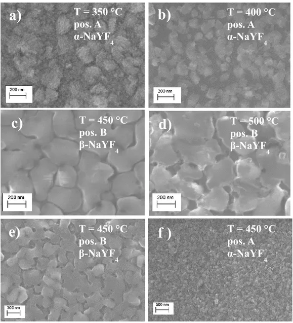
In addition, metal organic chemical vapor deposition method has been successfully applied for the synthesis of NaYF4 and KYF4 thin films. The fluorinated
“third-generation” bimetallic precursors NaY(hfa)4•tetraglyme, synthetized in a previous
work (vide infra), and the novel KY(hfa)4•tetraglyme have been the starting point
and the preliminary results confirm that the MOCVD approach yields reproducibly and selectively the synthesis of films of the pure KYF4 phase and of the pure
hexagonal NaYF4 phase, which show the best host behavior for the Ln doping ions
compared to the cubic structure, and without any impurity.
These final goals have been achieved through an accurate optimization of the operative parameters, such as the deposition temperature, the vaporization temperature of the precursors, the choose of the substrates and their positions inside the reactor.
Structural, morphological, and compositional characterization of the films shows the formation of polycrystalline thin films with a very uniform surface and suitable doping. In fact, an appropriate tuning of the mixture composition for the lanthanide
33
doped CaF2 system, i.e. the Ca:Ln ratio in the multicomponent source, permits the
deposition of films with the desired stoichiometry. The Ln3+ doped CaF2 films show
promising up-conversion properties in the visible and near infrared regions upon laser excitation for different doping mixtures.
2.1 Introduction
Alkaline earth fluoride materials have attracted great attention due to a wide variety of applications in dielectrics, optics, optoelectronics, and photonics [1–4]. In particular, alkaline earth fluoride such as MF2 (M: Ca, Sr) and MREF4 (M: Na, K; RE:
Y, Gd) has been regarded as the most efficient hosts for up-conversion (UC) or down-conversion emissions, also due to their low phonon energy, which minimize non-radiative de-excitation processes [5–8]. UC and DC processes could enhance the efficiency of photovoltaic devices since it makes possible to collect the radiation energy outside the absorption range of the photoactive material (usually silicon) by shifting its energy to a more suitable optical region. In addition, rare-earth doped fluoride compounds are promising luminescent materials as phosphors and in technological applications as micro- and nanoscale thermometry for microelectronics and for biomedical assays [9–11].
Several studies are available on the deposition methods applied for fabrication of alkaline earth fluoride films such as sputtering [12,13], atomic layer deposition [14], molecular beam epitaxy [15,16], sol–gel chemical routes [17]. Nevertheless, the metal organic chemical vapor deposition (MOCVD) has the potential advantage of being a very reliable and reproducible method for the fast production of films with high uniformity degree in both thickness and composition over large areas.
MOCVD has been already applied to the deposition of the fluorite films; nevertheless, most of these reports used a fluorine-free calcium source, thus a second precursor is needed as the fluorine source [18].
34
2.2 Ln3+ doped CaF2 thin films: MOCVD fabrication and their up-conversion
properties
In this study, we report for the first time the synthesis of CaF2 films doped with
Yb3+,Er3+ or Yb3+,Tm3+ through a simple MOCVD route on various substrates using a
molten mixture consisting of the Ca(hfa)2•diglyme•H2O and the suitable
Ln(hfa)3•diglyme [Ln = Yb, Er, Tm; Hhfa = 1,1,1,5,5,5-hexafluoro-2,4-pentanedione;
diglyme = 2-methoxyethyl ether] precursors in an appropriate stoichiometric ratio (structures in fig. 1).
Fig. 1 Ca(hfa)2•diglyme•H2O and Ln(hfa)3•diglyme structures.
The advantages of the present approach are various:
I. the metal precursors represent also a source of fluorine, thus avoiding the use of harmful hydrogen fluoride (HF) or other fluorine sources during the deposition step;
II. the application of all the required metal precursors in a unique multicomponent mixture allows for an easy control of the precursor source by simply adjusting the stoichiometric ratio;
35
III. the use of the same polyether (diglyme) to complete the coordination sphere of calcium and lanthanide ions avoids the undesirable potential ligand exchange.
The structural, morphological, compositional, and luminescent properties point to the formation of good quality CaF2 films with promising up-conversion properties
reflecting the correct stoichiometry of the films. The films were deposited on glass, quartz, and Si (100) substrates.
Given the same nature of the ligand and similar vaporization temperature ranges of the single precursors [19-21], no ligand exchange occurs and an efficient vaporization without thermal degradation takes place.
2.2.1 Experimental Section
The Ln(hfa)3•diglyme precursors were synthesized as previously reported in refs.
[19] and [22]. The Ca(hfa)2•diglyme•H2O adduct has been prepared through a
one-step reaction from the calcium oxide, Hhfa and diglyme ligands in dichloromethane under refluxing. The synthesis has been carried out starting from the CaO (0,40 gr; 0.71×10⁻²mol) suspended in dichloromethane (40 ml) with diglyme (0,770 ml, 0,71×10⁻²
mol) and H-hfa (1ml, 1.42×10⁻²mol). The mixture was refluxed, under stirring, for 90
min. The solution was collected by filtration under vacuum and the excess of CaO was filtered off. White crystals were obtained upon evaporation of the solvent, were washed two times in pentane and recovered by filtration.
The films were deposited on glass, quartz, and Si (100) under low-pressure in a horizontal hot-wall reactor, in the 450–550 °C temperature range. An appropriate ratio of the Ca, Yb, and Er (or Tm) complexes were used at 120°C, a suitable temperature for an efficient vaporization without thermal degradation. Under this condition the source is a molten mixture, since the Ca(hfa)2•diglyme•H2O and
Ln(hfa)3•diglyme melt in the 106–109 °C and 72–76 °C ranges, respectively. Heating
36
reservoir, respectively. Argon was used as a carrier gas, while oxygen as the reactant gas was introduced in the main flow into close proximity to the reaction zone.
Film structure was analyzed by XRD in glancing incidence mode (0.5°) using a Smartlab Rigaku diffractometer, equipped with a rotating anode of Cu Kα radiation operating at 45 kV and 200 mA. Film morphology was analyzed by FE-SEM using a ZEISS SUPRA 55 VP field emission microscope. The films deposited on Si were analyzed as-dep, while films deposited on glass or quartz were Au-coated prior FE-SEM characterization. The EDX spectra were recorded using an INCA-Oxford windowless detector, having a resolution of 127 eV as the full width half maximum (FWHM) of the Mn Kα.
For the luminescence characterization, the samples were excited at 980 nm using a diode laser as the source (CNI Optoelectronics Tech), with an intensity of 3.2 W mm−2. The emission spectra were detected by a Black Comet SR Spectrometer
(StellarNet Inc), with optical spectral resolution of 1 nm.
2.2.2 Results and discussion
XRD analysis
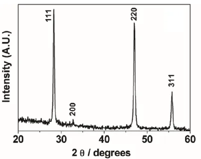
The X-ray diffraction (XRD) analysis of the samples CaF2: Yb 18%, Er 2% (mol % with
respect to the total metal content) deposited at 500°C on Si (100) exhibits patterns associated with a cubic CaF2 phase (ICDD No. 35-0816) (fig. 2). The diffraction
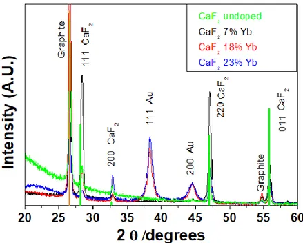
features observed at 2θ values of 28.25°, 32.75°, 47.00° and 55.75° are associated with the 111, 200, 220, and 311 reflections, respectively. The XRD measurements of films deposited at lower and higher temperatures and on different substrates show similar patterns. A closer look to the patterns, recorded with a 0.02° resolution, of films containing different amounts of Yb3+ ions reveals a small shift of the peak positions
with respect to those found for the undoped CaF2 film (fig. 3). A magnification of the
37
CaF2 220 peak; a slight shift toward higher angles is found for all the Yb3+ doped CaF2
films.
This behavior may be correlated on the one side to the ionic radii of the involved doping ions and on the other hand to the need of charge balance due to the different charge 2+ of calcium and 3+ of lanthanide ions, which can be compensated with additional fluoride ions.
38
Fig. 3 XRD patterns of CaF2 films doped with different amount of Yb: undoped, 7%,18% and 23%.
Fig. 4 A magnification of the 220 reflection of the CaF2 films doped with different amount of Yb.
The lanthanide ions are supposed to substitute calcium, thus assuming an eight coordination, considering that the Ca2+ and Ln3+ ions have similar ionic radii, with
39
coordination [23]. In particular, the Yb3+, Er3+, and Tm3+ ions have ionic radii of 0.985,
1.004, and 0.994 Å, respectively (in eightfold coordination) [23], slightly smaller than the Ca2+ ions. Therefore, a mere effect due to substitution of Ca2+ by Ln3+ ions gives
rise to a shift toward higher 2θ angles.
The a-axis parameters of the CaF2: Yb, Er films and for an undoped MOCVD-grown
CaF2 film have been determined as average of all the values obtained from the
individual reflections by using the relationship between hkl and the lattice parameter for a cubic structure, and they are reported in Table 1 as a function of the ytterbium doping. In this context, it is worth mentioning that the a-axis parameter has been estimated using graphite as an internal standard.
Table 1. Values of the a-axis parameters of the CaF2:Yb3+, Er3+ films grown on quartz at 500 °C.
The energy dispersive X-ray (EDX) analysis confirms that the Yb3+ ions are
incorporated in the films, but further experiments are needed to clarify the reason of the observed similarity between the a-axis parameter for the two 18% and 23% ytterbium doped films. The decrease of the a-axis parameter may be related to the slight smaller ionic radius of Ln3+ vs Ca2+ and it clearly indicates that the lanthanide
ions are incorporated in the crystalline lattice. Nevertheless, both the difference of the ionic radii of the metal ions and the effect of the charge compensation, which could
40
be satisfied by the insertion of interstitial fluoride ions or clusters, has to be considered to explain the peak shift.
In addition, thermal stresses between CaF2 films and the Si substrate, due to the
considerable difference in their thermal expansion coefficients (vide infra), could have effect in the lattice parameter of the deposited films. This effect has been deeply studied in the morphologic characterization and the optimized parameters of time deposition (60 min), and cooling rate (3 °C•min−1) from deposition temperature to
room temperature, yields crack-free films on Si and thickness of about 500nm.
EDX analysis
Quantitative EDX analysis confirms a uniform stoichiometry on the whole surface for all the films and for all the deposition temperatures. The EDX spectrum of a film deposited at 500 °C (fig. 5) shows the L and M lines of ytterbium, the Kα and Kβ peaks of calcium, the Kα peak of fluorine, and the Kα peak of the silicon substrate. The erbium and thulium peaks, relative to the nominal concentration of 2%, are scarcely detectable, due to their low concentrations that are on the borderline of the detection limit of the EDX technique. It is worthy of noting the absence of C and O, whose Kα peaks should appear at 0.277 and 0.525 keV, respectively.
The concentrations of the dopants, typically used for efficient UC emission [24] of 18% of ytterbium and 2% of erbium or thulium for the CaF2 doped films, are found
through EDX in samples deposited at 500°C. An accurate evaluation of the deposition temperature effect on atomic composition of the Ln dopants in the films has been done through EDX characterization. At temperatures of 450 °C the percentage of Ln3+ found in the films is higher than about 20% compared to the
expected value based on the initial composition of the precursor mixture. On the contrary, at temperatures of 550 °C, the percentage of Ln3+ found is lower than about
18%. Finally, at deposition temperature of 500 ° C the percentage composition of the doping ions obtained is the same of that initially set. Therefore, the doping amount increases upon increasing the deposition temperature and, on the contrary, decreases
41
at temperatures lower than 500°C. This finding may be related to a different decomposition behavior of the precursors, i.e., the Ca precursor likely decomposes more easily at lower temperature, so the net result is a major amount of Ca with respect to Ln, which reflects on the lower doping ratio observed at the lower temperature. In any case, the deposition temperature permits an accurate tuning of the stoichiometry, and an appropriate tuning of the mixture composition, i.e., the Ca:Ln ratio in the multicomponent source, permits the deposition of films with a desired stoichiometry at whatever temperature.
Fig. 5 EDX spectrum of the CaF2: Yb(18%), Er(2%) film deposited at 500 °C on Si (001).
FE-SEM characterization
Microstructure and morphology of CaF2 films have been studied by field emission
scanning electron microscopy (FE-SEM). The FE-SEM images of the films deposited on Si (100) do not show a homogeneous surface. Film deposited at 500 °C for 90 min (fig. 6a) shows some swelling, while films deposited for 60 min show a significant cracking as observed in fig. 6b. These effects are likely due to the considerable difference in the thermal expansion coefficients of the CaF2 film and that of the Si