A
LMA
M
ATER
S
TUDIORUM ·
U
NIVERSITÀ DI
B
OLOGNA
Scuola di Scienze
Corso di Laurea Magistrale in Fisica
In-‐situ detection of defect formation
in organic flexible electronics
by Kelvin Probe Force Microscopy
Relatore:
Presentata da:
Prof.ssa Beatrice Fraboni
Lorenzo Travaglini
Correlatore:
Dott. Tobias Cramer
Sessione I
Anno Accademico 2014/2015
Sessione III
Anno Accademico 2014/2015
Abstract
Organic semiconductor technology has attracted considerable research interest in view of its great promise for large area, lightweight, and flexible electronics applications. Owing to their advantages in processing and unique physical (i.e., electrical, optical, thermal, and magnetic) properties, organic semiconductors can bring exciting new opportunities for broad-impact applications requiring large area coverage, mechanical flexibility, low-temperature processing, and low cost. Thus, organic semiconductors have appeal for a board range of devices including transistors, diodes, sensor, solar cells, and light-emitting devices. In order to improve the resistance of organic electronics to mechanical strain and to achieve highly flexible device architecture it is crucial to understand on a microscopic scale how mechanical deformation affects the electrical performance of organic thin film devices. Towards this aim, I established in this thesis the experimental technique of Kelvin Probe Force Microscopy (KPFM) as a tool to investigate the morphology and the surface potential of organic semiconducting thin films under mechanical strain.
KPFM has been employed to investigate the strain response of two different organic thin film transistors with organic semiconductor made by 6,13-bis(triisopropylsilylethynyl)-pentacene (TIPS-Pentacene), and Poly(3-hexylthiophene-2,5-diyl) (P3HT) respectively. The results show that this technique allows to investigate on a microscopic scale failure of flexible thin film transistors with this kind of materials during bending. I find that the abrupt reduction of TIPS-pentacene device performance at critical bending radii is related to the formation of nano-cracks in the microcrystal morphology. The cracks are easily identified due to the abrupt variation in surface potential caused by local increase in resistance. Numerical simulation of the bending mechanics of the hole transistor structure further identifies the mechanical strain exerted on the TIPS-pentacene micro-crystals as the fundamental origin of fracture.
Instead for P3HT based transistors no significant reduction in electrical performance is observed during bending. This finding is attributed to the amorphous nature of the polymer giving rise to an elastic response without the occurrence of crack formation.
Abstract
La tecnologia basata sui semiconduttori organici ha suscitato un notevole interesse nell’ambito della ricerca in vista delle sue promettenti applicazioni nell’elettronica flessibile quali ricoprire vaste aree, leggerezza e flessibilità. A causa dei loro vantaggi operativi e proprietà fisiche uniche (elettriche, ottiche, termiche e magnetiche), i semiconduttori organici possono portare nuove opportunità per le applicazioni ad ampio impatto che richiedono ampia area di copertura, lavorazione a bassa temperatura e basso costo. Così, i semiconduttori organici hanno applicazione in una vasta gamma di dispositivi tra cui transistor, diodi, sensori, celle solari, e dispositivi emettitori di luce. Per migliorare la resistenza dell’elettronica organica a sollecitazioni meccaniche e per realizzare architetture dei dispositivi altamente flessibili è fondamentale comprendere in scala microscopica come la deformazione meccanica influisce sulle prestazioni elettriche dei dispositivi organici a film sottile. A tale scopo, ho stabilito in questa tesi la tecnica sperimentale Kelvin Probe Force Microscopy (KPFM) come uno strumento per indagare la morfologia e il potenziale di superficie dei semiconduttori organici a film sottile sotto sollecitazioni meccaniche.
La tecnica KPFM è stata impiegata per studiare la risposta alle sollecitazioni meccaniche di due differenti transistor a film sottile con la regione attiva costituita da 6,13-bis(triisopropylsilylethynyl)-pentacene (TIPS-Pentacene), e Poly(3-hexylthiophene-2,5-diyl) (P3HT) rispettivamente. I risultati mostrano che questa tecnica è utile ad indagare in scala microscopica problematiche dei transistor a film sottile flessibili, con questo tipo di materiali, durante la piegatura.
Ho trovato che la brusca riduzione delle prestazioni del dispositivo con TIPS-Pentacene a certi raggi di curvatura è legata alla formazione di nano-cracks nella morfologia dei micro cristalli per il caso del film costituito da TIPS-Pentacene. I crack sono facilmente identificabili a causa della brusca variazione del potenziale di superficie causata da un aumento locale della resistenza.
Simulazione numerica della meccanica del piegamento della struttura del transistor identifica ulteriormente le sollecitazioni meccaniche sui micro cristalli di TIPS-Pentacene come origine fondamentale della frattura.
Per il caso dei transistor basati sul P3HT non si nota una significativa riduzione delle prestazioni del dispositivo durante il piegamento. Questa osservazione è attribuita alla natura amorfa del polimeriche da luogo ad una risposta elastica senza il verificarsi di una formazione di crepe.
Contents
INTRODUCTION ... 1
1
FLEXIBLE ORGANIC ELECTRONICS ... 3
1.1 INTRODUCTION TO ORGANIC MATERIALS ... 3
1.2 ORGANIC SEMICONDUCTORS ... 8
1.3 CHARGE CARRIER TRANSPORT IN ORGANIC MATERIALS ... 11
1.4 THIN FILM TRANSISTORS ... 13
1.5
6,13-BIS(TRIISOPROPYLSILYLETHYNYL)PENTACENE ... 17
1.6 POLY(3-HEXYL)THIOPHENE (P3HT) ... 18
2
KELVIN PROBE FORCE MICROSCOPY ... 19
2.1 AFM IN NON-CONTACT MODE ... 19
2.2 ELECTROSTATIC FORCE MICROSCOPY ... 23
3
MATERIALS AND METHODS ... 29
3.1
TFT STRUCTURES ... 29
3.2 TRANSISTOR CHARACTERIZATION ... 30
3.3
DEFORMATION OF TFT ... 31
3.3.1
Setup for mechanical deformation ... 32
3.3.2
Simulation of mechanical deformation ... 34
3.4 KELVIN PROBE FORCE MICROSCOPY ... 34
3.5 IMAGE ANALYSIS ... 36
3.6
EXPERIMENTAL PROTOCOL ... 36
4
RESULTS AND DISCUSSIONS ... 39
4.1
MECHANICAL DEFORMATION OF TFT ... 39
4.2 TIPSPENTACENE ... 42
4.2.1
unstressed tips pentacene TFT i-v characteristic and microscopic analysis ... 43
4.2.2
stressed TIPS-Pentacene TFT i-v characteristic and microscopic analysis ... 46
4.3
P3HT ... 53
5
CONCLUSION AND OUTLOOK ... 57
Introduction
With the invention of the transistor around the middle of the last century, inorganic semiconductors such as Si or Ge began to take over the role as the dominant material in electronics from the previously dominant metals. At the same time, the replacement of vacuum tube based electronics by solid state devices initiated a development, which by the end of the 20th century has led to the omnipresence of semiconductor microelectronics in our everyday life. Now at the beginning of the 21st century we are facing a new electronics revolution that has become possible due to the
development and understanding of a new class of materials, commonly known as organic semiconductors.
The transistor is a fundamental building block for all modern electronics; transistors based on organic semiconductors as the active layer are referred to as organic thin film transistors (OTFTs). A number of commercial opportunities have been identified for OTFTs, including flat panel active-matrix liquid crystal displays (LCDs) or active matrix organic light-emitting diodes displays (AMOLEDs), electronic paper (e-paper), low-end data storage such as smart cards, radio-frequency identification (RFID) and tracking device, low-cost disposable electronic products, and sensor arrays; more application continue to evolve as the technology matures.
The unique features, which give organic electronics a technological edge, are simpler fabrication methods and the ability to withstand mechanical forces related to flexing or stretching. Fabrication of organic electronics can be done using relatively simple processes such as evaporation, spin-coating, and printing, which do not require high-end clean room laboratories.
Flexibility, or, in other words, the possibility of adapting the fabricated devices on different kinds of substrates, is certainly one of the main advantages of this new technology. For this reason, many efforts have been recently made to develop flexible OTFT systems for applications in which devices are continuously exposed to mechanical stress, such as, for instance, in wearable electronics. As a matter of fact, organic semiconductor based device are severely affected by mechanical deformation. In particular, the surface strain induced on the active layer usually gives rise to pronounced variations in the conductivity of the device.
This feature in some cases was used for the fabrication of OFET-based mechanical sensors; on the other hand, there are many applications in which this mechanical sensitivity is undesired, because device are required to operate normally even during mechanical deformation. Therefore, investigating the mechanical properties of organic semiconductor is of a crucial importance for addressing the different requirements of these applications.
In order to shed some light on the mechanical sensitivity of OFETs, many efforts have been aimed towards the investigation of the main causes that lead organic semiconductors to be sensitive to mechanical stress [1][2][3]. In many cases, the current variation can be correlated to morphological changes taking place in the active layer, thus modifying the hopping energy barrier for charge transport [1][2].Very recently, a correlation was observed between the device electrical behaviour and the modification of the structural properties of the structural properties of the organic active film induced by the mechanical deformation. Moreover it was recently demonstrated by comparing OTFTs realized using two different classes of organic semiconductors, that the intrinsic morphological properties of the organic semiconductor film can dramatically influence the sensitivity of mechanical deformation of the devices.
In this thesis I investigated the microscopic details of these aspects on OFETs with two different types of material for the active region, in particular with TIPS Pentacene and P3HT. I established KPFM as a tool to study morphology, surface potential during mechanical strain. These microscopic investigations were combined with the electrical characterizations of the macroscopic devices with the aim of revealing a possible correlation between morphological properties and device sensitivity to mechanical deformation.
The first chapter of this thesis illustrates the general properties of organic materials and discussing the charge transport mechanism of organic semiconductors.
The second chapter contains an introduction to atomic force microscopy with special emphasis on the non-contact interaction regime and Kelvin Probe Force Microscopy described.
The third chapter describes the general procedures adopted throughout the experimental work, including the description of the typical TFT structure used, the sample preparation, the measurement setup and other methods. The fourth chapter reports the characterization results of the related sample and a discussion of the findings and further implications.
1 Flexible Organic Electronics
In this chapter, the fundamental properties of organic materials is introduced in section 1.1. Among the organic materials, organic semiconductors are the basis of organic electronics and their most important properties will be treated in subsection 1.2, and the charge transport mechanism of these materials will be illustrated. Section 1.3 and 1.4 describes the electrical characteristics of organic thin film transistors (OTFT) used in these experimental work. In section 1.5 and 1.6 a brief description of the materials used as the active layer of devices [4]-[5].
1.1 Introduction to organic materials
The term “organic semiconductors” is not new. First studies of the photoconductivity of anthracene crystals (prototype of organic semiconductors) were undertaken in early 20st century. The discovery of electroluminescence in the 1960s gave an incentive to study thoroughly the properties of molecular crystals. These studies, however, have only contributed to a better understanding of the theoretical basis of optical excitation and electric charge transfer in organic materials, rather than solve the problems that precluded the use thereof on an industrial scale (low stability, low electric and luminous efficiency). It was only the successful synthesis and controlled polymer doping, for which the Nobel Prize in chemistry was awarded in 2000, that opened up new area of application for organic conducting materials [6].
The adjective organic used in the expression organic electronics refers to the fact that, in this branch of electronics, the active materials used for the fabrication of devices is organic compounds. Although the distinction between ’organic’ and ’inorganic’ compounds is not always straightforward, an organic molecule is usually defined as a chemical compound containing carbon [7]. For historical reasons, this definition does not include a few types of carbon-containing compounds (such as carbonates, simple oxides of carbon and cyanides, as well as the allotropes of carbon such as diamond and graphite), which are therefore considered inorganic. Consequently, in order to explain and understand the electrical properties of organic compounds it is necessary to describe the electronic configuration of the carbon atom and the way it forms chemical bonds with other atoms (of the same type or belonging to different chemical species). Carbon is an element belonging to the Group 14 of the periodic table. The members of this group are characterised by the fact that they have four electrons in the outer energy level.
There are three naturally occurring isotopes of carbon: carbon-12, carbon-13 and carbon-14 (the number following the element name indicates the total number of neutrons and protons contained into the atom nucleus). Carbon-12 (whose nucleus is formed by six neutrons and six protons) is the most stable of all three isotopes and is also the most abundant, accounting for the 98.89 % of carbon. In this thesis, whenever the name “carbon” is used, the isotope carbon-12 will always be implicitly referred to.
In order to understand the electronic properties of organic compounds it is essential to describe the way carbon electrons are distributed in space and the way they are bonded to the nuclei [8]. In other words, it is necessary to introduce the concepts of atomic orbital and orbital hybridisation. According to quantum mechanics [9], the wave-like behaviour of an electron may be described by a complex wave function depending on both position and time Ψ(r, t); the square modulus |Ψ|2 is equal to a probability density: the integral of the square modulus over a certain volume V gives the probability of finding, at a certain instant t, the electron in that volume.
Let us consider now the following equation:
𝛹(𝑟, 𝑡)!𝑑𝑥𝑑𝑦𝑑𝑧 ≥ 0.9
!
(1.1)
Equation (1.1) defines a volume Ω in which the probability to find an electron (described by Ψ(r, t)) is at least the 90%; such a region in space is called atomic orbital and its shape depends on how Ψ is mathematically defined.
Figure 1.1: shape of the first five orbitals
Each orbital is defined by a different set of quantum numbers and contains a maximum of two electrons. The shape of each orbital depends on the mathematical definition of the wavefunction and
therefore on the value assumed by the l quantum number. In Figure 1.1 illustrates the shape of the first five orbitals:
The first two orbitals on top of Figure 1.1 are respectively the orbitals 1s and 2s; they are shaped as spheres centred in correspondence with the atom nucleus. The three orbitals on the bottom are the 2p orbitals; each one of them is shaped as a couple of ellipsoids with a point of tangency in correspondence with the atom nucleus. The three p orbitals are reciprocally orthogonal: if we consider a cartesian coordinate system centred in the nucleus, these orbitals appear aligned along the three axes and are therefore called 2px, 2py and 2pz orbitals.
As mentioned previously, carbon belongs to the Group 14 of the periodic table. It is actually the simplest element of its group, having just six electrons: two of them are contained into the 1s orbital, while the other four are hosted by the second electron shell. When carbon is in its ground state (that is lowest energy state) two of the outer electrons are placed into the 2s orbital while the two remaining electrons are located in two of the 2p orbitals (let us assume, for instance, in 2px and 2py). According to the standard rules set by IUPAC [19], the ground-state electron configuration of carbon may be expressed by the following notation: 1s22s2 2px1 2py2 or, in a more compact fashion, 1s2 2s2 2p2 [5].
Chemical elements interact with one another through the formation of chemical bonds. From the point of view of organic chemistry, the most important chemical bond is the covalent bond. A covalent bond occurs when two atoms share a pair of electrons; this bond forms when the bonded atoms have a lower total energy than that of widely separated atoms. The formation of a covalent bond requires the partial overlap of two atomic orbitals; the shared electrons have a higher probability to be located in the area between the two atoms nuclei, where the overlap is maximum.
In certain cases, however, the structure of a molecule may not be explained if one considers the orbital shapes previously described. Let us examine, for instance, the simplest organic molecule, namely methane, CH4 (Figure 1.2)
Figure 1.2: Scheme of methane molecule CH4.
As can be seen from Figure 1.2, methane is characterised by a tetrahedral geometry, in which the carbon atom occupies the tetrahedron centre while the four hydrogen atoms are placed in correspondence with the four-tetrahedron corners. This geometry is not compatible with the orbitals depicted previously; in particular, the three 2p orbitals cannot be geometrically arranged to fit a tetrahedral structure. Linus Pauling solved this problem in 1931, in a famous paper [10] in which the
theory of orbital hybridisation was described for the first time. The concept of orbital hybridisation can be explained as follows. Let us take n different orbitals, each one described by its own wavefunction Ψi(r, t); when hybridisation occurs, these orbitals are linearly combined in order to form
n new hybridised orbitals, each one corresponding to its own wavefunction Φj(r, t) as shown in the
following formula:
𝛷! 𝑟, 𝑡 = 𝑐!"𝛹!(𝑟, 𝑡) !
!!!
( 1.2 )
Where coefficients cij are usually determined to ensure that the wavefunctions describing the
hybridised orbitals must be normalised (the integral over all space of their square modulus must be equal to 1), and to guarantee all hybridised orbitals must have the same energy.
From a qualitative point of view, hybridisation may be thought of as a “mix” of an atom orbitals which results in the formation of new, isoenergetic orbitals more suitable for the description of a specific molecule structure.
That being said, the particular structure of methane may be explained if one considers the hybridisation of carbon outer orbitals (namely, 2s and the three 2p orbitals) which results in the formation of four sp3 orbitals, as shown in Figure 1.3: the four sp3 orbitals of carbon partially overlap with the 1s orbitals of hydrogen atoms, giving rise to four covalent bonds which are usually indicated as σ-bonds. Other organic molecules show geometrical characteristics which can be explained only considering other forms of hybridisation.
Figure 1.3: Sp3 hybridisation scheme.
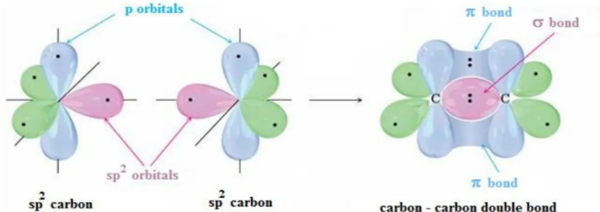
The hybridization sp2 takes place, for instance, in the ethylene molecule CH2=CH2 (Figure 1.4):
Ethylene is a planar molecule whose structure cannot be explained if one considers the original set of carbon orbitals or an sp3 hybridisation. Indeed, the carbon atoms of ethylene (as well as of all other
compounds where a double C=C bond is present) are characterised by another form of orbital hybridisation, called sp2 hybridisation where, the 2s orbital and two 2p orbitals (let us assume 2px and 2py) hybridise and form a set of three sp2 orbitals which lie on the XY plane and are located in
correspondence with the corners of an equilateral triangle (Figure 1.5).
The fourth, unhybridised 2pz orbital lies along a direction which is perpendicular to the plane
containing the hybridised sp2 orbitals.
Figure 1.4: Ethylene molecule.
Figure 1.5: Sp2 hybridization
When two sp2-hybridised carbon atoms come into close contact in order to form a chemical bond, the orbitals overlap occurs at two different levels. On one hand, one can notice the formation of a covalent σ -bond resulting from the intersection between two sp2 orbitals along the line joining the two carbon atoms’ nuclei. The other two sp2 orbitals overlap with the hydrogen atoms’ 1s orbitals and
form two other covalent σ -bonds. When the two carbon atoms come into contact, a partial overlap between the two unhybridized 2pz orbitals occurs.
This overlap is responsible for the formation of a second covalent bond between the carbon atoms, called π bond. These two types of covalent bond are shown in the following picture (Figure 1.6).
Figure 1.6: formation of carbon-carbon double bound π and σ.
It should be noted that π bonds are less energetic than σ bonds (about 65 kcal/mol versus 80 kcal/mol)1. This is essentially due to the fact that, geometrically speaking, a σ bond is characterised by a much larger overlap volume, which causes a stronger constructive interference between the orbitals responsible for the formation of the bond. This phenomenon has very important consequences for the electrical behaviour of the molecule: while σ electrons are strictly confined into the small volume between the two carbon atoms’ nuclei, π electrons are able to move into a larger volume and their interaction with the nuclei is relatively weak1.
1.2 Organic semiconductors
Carbon is a chemical element showing an ability which is almost unique: the capability to form covalent bonds with other carbon atoms and create macromolecules represented by very long chains or more complex structures such as nets. This property is called catenation. Since many organic compounds used in organic electronics are polymers, which are macromolecules obtained through this catenation process, in order to understand the behaviour of organic electronic devices it is necessary to define exactly what polymers are and examine shortly their properties.
According to the definition provided by IUPAC, a polymer may be defined as a molecule of high relative molecular mass, composed of repeating structural units called monomers, characterised by a low relative molecular mass and are interconnected typically by means of covalent bonds.
1
Carbon also shows a third type or orbital hybridisation called sp hybridisation which leads to the formation of carbon-carbon triple bonds (one σ bond together with two π bonds). From our point of view, this hybridisation is not particularly relevant and therefore will not be described or mentioned in the rest of the thesis.
It is not at all easy to provide general guidelines for the characterisation of a polymer, considering the enormous number of chemical compounds that have been synthesised. However, some classification parameters do exist:
• the chemical characteristics of the composing monomer(s);
• the morphology of the single polymer molecule, that is the geometrical structure formed by the monomers connection (for instance, linear versus branched chain);
• the average molecular weight of a single polymer molecule; • tacticity (the spatial orientation of the chain’s side groups);
• the polymer morphology (the way polymer molecules are spatially arranged in a film or solid);
This last point is extremely important because many electrical transport properties are strictly connected to the morphological features of the polymeric layer. The crystallinity of a polymeric solid is in fact a very important parameter because, as will be shown in the following paragraphs, the conduction behaviour of a polymer is strictly connected to its morphology.
Electronics may be defined as that branch of Physics which studies electronic phenomena occurring within closed paths (electric circuits) designed to carry, manipulate or control electron flow for some purpose. In order to understand how organic devices work it is therefore essential to have a clear picture of the conduction mechanisms in organic conductors and semiconductors.
More specifically, conductive polymers are usually defined as organic polymers able to conduct electricity, exhibiting a conductive or a semiconductive behavior. Conductive polymers can be roughly grouped into three different categories:
• conjugated polymers;
• polymers containing aromatic cycles;
• conjugated polymers containing aromatic cycles.
All the molecules belonging to the previous categories have in common the alternation of single and multiple bonds (usually, double bond) in their structure. This is shown for example, in Figure 1.7, for the simplest conjugated molecule, polyacetylene.
Figure 1.7: Polyacetilene molecule scheme, the simplest example of conjugated molecule.
As can be clearly seen from the picture above, the chain structure of molecules like polyacetylene may be thought of as a sequence of carbon atoms in which sp3-hybridised carbon atoms are alternated
Thanks to this continuous orbital overlap, π electrons (which are loosely bound to the atoms’ nuclei) are able to flow along the polymer chain when a voltage is applied to the molecule’s extremities, thus enabling the polymer itself to conduct electricity.
A quantitative description of conductivity phenomena in conjugated polymers may be provided through the theory of Molecular Orbitals (MOs). According to this theory, the orbital of a complex molecule (MO) may be expressed starting from the wave functions describing the orbitals of the atoms (AOs) which compose the molecule. From a mathematical point of view, this is usually done by expressing the MO as a linear combination of the AOs; this approach is known through the acronym LCAO (Linear Combination of Atomic Orbitals).
In these molecules, because of this orbitals overlapping, the arrangement of the electrons is reconfigured concerning the energy levels. We can separate the molecular energy levels into two categories: π and π*, bonding and anti-bonding respectively, forming a band-like structure (Figure 1.8). The occupied π-levels are the equivalent of the valence band in inorganic semiconductors.
Figure 1.8: The formation of a MO may be graphically described by means of an energy diagram in which the three energy levels (energy of single atoms, energy of bonding MO and energy of anti-bonding MO are
reported).
The electrically active level is the highest one and it is called Highest Occupied Molecular Orbital (HOMO). The unoccupied π*-levels are equivalent to the conduction band. In this case, the electrically active level is the lowest one, called Lowest Unoccupied Molecular Orbital (LUMO). The resulting band gap is given by the difference of the energy between HOMO and LUMO.
If we consider a polymer chain with N atoms using the quantum mechanical model for a free electron in a one dimensional box, the wave functions for the electrons of the polymer chain is given by:
𝐸!= 𝑛!ℎ! 8𝑚𝐿!
(1.3)
with n=1, 2, 3 etc…and where h is the Plank constant, m the electron mass and L the conjugation length, which, if we consider N atoms separated by a distance d within the polymer chain, is equal to Nd. Therefore, if the π-electrons from the p-orbitals of the N atoms occupy these molecular orbits, with 2 electrons per orbit, then the HOMO should have an energy given by:
𝐸 𝐻𝑂𝑀𝑂 = 𝑁 2 ! ℎ! 8𝑚𝐿! (1.4)
whereas, the LUMO will have an energy of:
𝐸 𝐿𝑈𝑀𝑂 = 𝑁 2 + 1 ! ℎ! 8𝑚(𝑁𝑑)! (1.5)
All energies are supposed to be measured with respect to vacuum energy level as reference. Thus, the energy required to excite an electron from the HOMO to the LUMO is give by their energies difference: 𝐸!= 𝐸 𝐿𝑈𝑀𝑂 − 𝐸 𝐻𝑂𝑀𝑂 = 𝑁 + 1 !ℎ! 8𝑚 𝑁𝑑 ! ≅ ℎ! 8𝑚𝑑!𝑁 𝑓𝑜𝑟 𝑙𝑎𝑟𝑔𝑒 𝑁 (1.6)
It is evident that the band gap is inversely proportional to the conjugation length L, and, as a consequence, to the number of atoms N in the polymer chain. If the band gap is high the material is an insulator, if it is low the material is a conductor. Usually the most of the organic semiconductors have a band gap between 1.5 to 3 eV.
1.3 Charge carrier transport in organic materials
Inorganic semiconductors such as Si or Ge, atoms are held together by very strong covalent bonds and charge carriers moves as highly delocalized plane waves in wide bands and usually have very high mobility.
However, when polymer molecules aggregate, the resulting polymeric solids exhibit different crystallinity degree, varying from almost perfect crystals to amorphous solids [11]. As a consequence,
charge carrier transport in such solids varies in a range delimited by two extreme cases: band transport and hopping.
Band transport is normally observed only in pure, single organic crystals [46]. In such materials, charge mobility depends on temperature according to the following power law:
µμ ∝ 𝑇!! 𝑤𝑖𝑡ℎ 𝑛 = 1 … 3 (1.7)
In highly disordered polymeric solids, such as amorphous solids, transport usually proceeds via hopping and is thermally activated. In amorphous solids, molecules are arranged in a random, disordered way. Therefore, energy states are not organised in continuous bands separated by an energy gap but instead localised energy states (i.e. existing only for discrete values of the wave number k) occur. The density of these states is usually described using a couple of Gaussian distributions, the Gaussian functions being centred in correspondence with the energy level where the majority of levels appear. The functions peaks may be interpreted as analogous to conduction and valence bands in crystalline semiconductors (Figure 1.9).
Figure 1.9:Energy diagrams in different types of organic semiconductors.
In amorphous solids, charge flow takes place when electrons start moving (hopping) from lower energy levels to higher energy levels. This flow is due to an increment in electrons energy which may be caused both by temperature or the application of an external electric field. A simple model frequently used in order to express mathematically the mobility dependence on the factors cited above is the following:
µμ 𝐹, 𝑇 ∝ exp −∆𝐼 𝑘𝑇 𝑒𝑥𝑝
𝛽 𝐹
𝑘𝑇 (1.8)
where ∆E is a parameter called activation energy (i.e. the minimum amount of energy to be provided in order to start conduction) and F represents the applied electric field. The case of semicrystalline polymeric solids is perhaps the most complicated, from an analytical point of view. These solids
usually assume a polycrystalline structure, in other words they may be thought of as many crystalline grains immersed into an amorphous matrix. While within the grains charges move thanks to band transport, the problem arises in correspondence with the grain boundaries. Here, mobile charges are temporarily immobilised (trapping) thus creating a potential barrier which electrostatically repels same sign charges; as a consequence, charge mobility is greatly decreased. A simple expression utilised in order to express mobility in polycrystalline semiconductors is given by the following:
µμ ∝ µμ!𝑒𝑥𝑝 −𝐸!
𝑘𝑇 (1.9)
In (1.9), µ0 is the mobility in crystalline grains and Eb is the height of potential barrier.
Even though the MOSFET laws are taken as representative also for OFETs, it is well known that, in most cases, the typical behaviour strongly differs from the ideal case. The main reason for such discrepancy is generally ascribed to the intrinsic structural properties of the organic semiconductors. Usually, when we grow an organic semiconductor film, we do not obtain a crystal structure; a single organic crystal can be obtained only under strict deposition conditions. Therefore, when we talk about organic semiconductors, we suppose to discuss about polycrystalline thin film, with a very hight concentration of structural defects which in the main reason for the non linearity usually observed in such devices. Every defect acts as scattering site for charge carriers, causing the distortion in the, ideally, periodic lattice potential. Therefore, a band-like transport is usually impeded by such scattering process. The effect of defects is even stronger if the defects themselves act as trapping sites for charge carriers. Trapping is relevant when the defect induces one or more energy levels in the band gap of the organic “crystal”. A charge carrier will prefer to occupy this lower energy level and the trap localizes the charge carrier in its site. The presence of traps within the semiconductor layer can cause a decrease in the density of mobile charges, since trapped carriers are localized at the defect sites. In some cases, when the density of defects is high and they strongly localize charge carriers, their influence can completely dominate charge transport across the semiconductor.
Several experiments have been performed on OFETs and several models have been introduced to study charge transport of both polycrystalline and crystalline active layers and its dependence to charge trapping. However, a universal theory which can properly describe charge transport in organic materials does not exist and transport properties are still not fully explained.
1.4 Thin film transistors
The interest for Organic Field Effect Transistors (OFETs) has drastically increased over the past few years, and they have been intensively studied for many application such as displays, smart tags and
sensors. The reason for focused research interest in the field of “plastic electronics” is the opportunity to produce low cost device on plastic substrates on large areas, opening, indeed, an entire market segment. So far, field effect mobilities up to 30 cm2/Vs have been reported for thin film and single
crystal OFETs. However, this value is usually lowered by at least one order of magnitude for organic transistor made on plastic substrates. OFETs are close relatives of the classic Metal Oxide Semiconductor Field Effect Transistors (MOSFETs); typically, since the organic semiconductors are characterized by a low conductivity if compared to inorganic ones, Thin Film Transistor (TFT) architecture is preferred in this case.
The core of an OFET is a Metal-Isulator-Semiconductor structure (MIS), which can in principle be considered as a parallel plate capacitor: the two capacitor plates are formed by a metal electrode, called gate electrode, and a semiconductor, which are separated by a thin insulating film, called gate dielectric (see Figure 1.10). Two additional electrodes, called Source and Drain electrodes are patterned in order to contact the organic semiconductor allowing to probe the conduction across the organic film.
Figure 1.10: Schematic of the OFETs geometry.
One of the main differences between an OFET and the classic MOSFET is that while the latter typically works in inversion mode, OFETs usually work in accumulation mode. When a negative (positive) voltage is applied between the gate and the source electrodes, an electric field is induced in the semiconductor that attracts positive (negative) charge carriers at the semiconductor/insulator interface overlapping with the gate. Applying a negative (positive) voltage between source and drain electrodes, it is possible to drive the positive (negative) charge carriers across the channel area. Charge transport in OFETs is substantially two-dimensional. Charge carrier accumulation is highly localized at the interface between the organic semiconductor and the gate dielectric, and the bulk of the material is hardly or not affected by gate induced field. Upon increasing gate voltage to positive (negative) values, the number of charge carriers accumulated in the channel will reduce until the
channel is fully depleted of free carriers. From this point on, negative (positive) charge are induced in the channel and the device should in principle work in inversion regime. In practise, the flowing current detectable in inversion regime is negligible because the number of charge carriers injected into channel is low due to the high injection barrier at the interface between metal electrodes/semiconductor. The boundary between accumulation and inversion regime is called threshold voltage VT of the device. Below the threshold voltage the device is in its off state, no free
charge carriers are present in the channel and no current flow across it.
Figure 1.11: Scheme of the TFT with parameters.
The geometric parameters needed to derive an expression for the current in a TFT starting from classical electrodynamics are illustrated in Figure 1.11. The first step is to estimate the charge dq induced by applying a voltage VG to the gate in an elemental strip of width dx at a distance x from the
source. Below threshold, the charge is zero. Above threshold, it becomes
d𝑞 = −𝐶! 𝑉!− 𝑉!− 𝑉(𝑥) 𝑊𝑑𝑥 (1.10)
Here, VT is the threshold voltage and V(x) the potential at the position x of the channel induced by the
application of the drain bias; V(x)=0 at the source and V(x)=VD at the drain. Ci is the capacitance per
unit area of the dielectric layer and W the channel width, so that Wdx represents the area of the elemental strip.
The minus sign at the right hand side of equation (1.10) arises from the fact that VG is applied to the
gate (one of the plate of the capacitor), while we are interested in the charge on the other plate (the conducting channel).
The current ID that flows between source and drain corresponds to the passage of the elemental charge
dq during the elemental time dt:
𝐼!= 𝑑𝑞 𝑑𝑡 = 𝑑𝑞 𝑑𝑥 𝑑𝑥 𝑑𝑡 (1.11)
The mobility µ is defined as the ratio between the mean velocity v=dx/dt of the charge carriers and the electric field E= −dV/dx, so that dx/dt=−µ(dV/dx). Making use of equations (1.10) and (1.11) can be rearranged as
𝐼!dx = 𝑊𝐶!𝜇 𝑉!− 𝑉!− 𝑉(𝑥) 𝑑𝑉 (1.12)
The drain current is now obtained by integrating equation (1.12) from source (x=0, V(x)=0) to drain (x=L, V(x) =VD). Assuming constant mobility, this leads to
𝐼!= 𝑊 𝐿 𝐶!𝜇 𝑉!− 𝑉!− 𝑉! 2 𝑉! (1.13)
Equation (1.13) corresponds to the so-called linear regime, where VD <VG−VT.As VD increases, the
voltage at the drain electrode gradually decreases, up to a point where it falls to zero.
This occurs at the so-called pinch off point, when VD = VG −VT. Beyond pinch off, a narrow depletion
zone forms next to the drain because the local potential there drops below threshold. Further increase of VD leads to a slight extension of the depletion zone and a subsequent shift of the pinch off point
towards the source. Because the potential at the pinch off point remains equal to VG −VT, the drain
current becomes independent of the drain voltage; this is the saturation regime. Here, the current is obtained by equating VD to VG –VT in equation (1.13):
𝐼!=
𝑊
2𝐿𝐶!𝜇 𝑉!− 𝑉! !
(1.14)
Because there are two independent voltages, the current–voltage curves of a transistor are of two sorts: in the output characteristic, a set of drain current versus drain voltage curves are drawn for various gate voltages; conversely, transfer characteristics are those in which the drain current is plotted as a function of the gate voltage for a given drain voltage. As will be seen in the following, parameter extraction is carried out from the latter set of curves.
The first examples of OFETs were hybrid structures, where the only “organic” part in the device, was the semiconductor. Typically, the first OFETs were assembled on highly doped silicon wafer, acting at the same time as substrate and as gate electrode. A thin SiO2 layer was employed as gate dielectric,
whereas metals (i.e. Au, Al) were used for the fabrication of the source and drain electrodes.
Nowadays, several examples have been reported concerning the realization of all organic FETs, where flexible plastic foil is generally used as flexible substrate, a polymeric gate dielectric (PVA or PVP or PMMA) is used instead of SiO2, and conductive polymers are employed as alternative to metals for
the patterning of the electrodes [12].
1.5 6,13-‐Bis(triisopropylsilylethynyl)pentacene
Acenes are a class of hydrocarbons consisting of a numbers of benzene rings; the Pentacene (C22H14)
belong to this class and, as is clear from name, it consist of five benzene rings (see Figure 1.12 (a)). This molecule is the basis of the most important organic semiconductor that are used for the manufacture of OFET (Organic-Field-Effect-Transistor). Despite this, e Pentacene is not an ideal material: its solubility is not appreciable, vacuum process are needed to deposit it, it oxidize easily and disturbs the transport and the crystallization process in the devices. Also it can condense in two crystalline phases which do not mate perfectly; for this reason often in the device grains are created which decrease the device performance. One of the most common way to solve these problems is tying to the Pentacene groups of molecules to get so many types of molecules including TIPS-Pentacene (6,13-Bis(triisopropylsilylethynyl)pentacene) (Figure 1.12 (b)).
Figure 1.12: (a) Pentacene molecule, (b) TIPS-Pentacene molecule.
The TIPS-Pentacene is soluble in a wide variety of organic solvents and oxidize goes more slowly then Pentacene: when is in solutions it remains stable in air for days and when it is in form of crystals remains stable for weeks. The problem of such a molecule is that it has randomly organization, for this reason deposition techniques are necessary to arrange the crystals in an orderly manner to increase the mobility.
1.6 Poly(3-‐hexyl)thiophene (P3HT)
Thiophene-based conjugated polymers have accompanied, if not originated, the interest in conductive polymer materials and their application in organic field-effect transistors (OFETs) and organic photovoltaic (OPV) devices. The most studied representative of this class of materials is poly(3-hexyl-thiophene) (P3HT) with its regioregular (head-to-tail) isomer.
Figure 1.13: poly(3-hexyl-thiophene) (P3HT).
The first polymerization reactions with high yield and small concentrations of synthesis impurities were reported in 1980. Solution-processed into thin films, these materials could exhibit reasonable conductivities limited, however, by the disorder that results from a regiorandom attachment of the side chains to the thiophene monomers. Like many conjugated polymers, P3HT is a polymorph, i.e., forms different crystal structures depending on processing conditions.
The most frequently observed are so-called forms I and II, which differ by the side chain conformation and interdigitation, inclination of conjugated backbones with respect to the stacking direction, and the shift of successive (along the π-stacking direction) polymer chains. Form I, which is observed after annealing, is the structure encountered in most studies dealing with OFETs and OPVs. On a mesoscale, crystallization from supercooled solutions in poor solvents can lead to the formation of secondary structures, notably nanofibers, with a width of tens of nanometers and length of several micrometers. OFETs active layer with P3HT may be sensitive to some wavelengths of light in the presence of oxygen. While this is not an acute problem for the bulk material, solutions and thin films tend to show some sensitivity over time. Therefore, storage and handling in an inert atmosphere (like nitrogen or argon) is recommended.
2 Kelvin Probe Force Microscopy
Kelvin probe force microscopy, or KPFM, was introduced as a tool to measure the local contact potential difference between a conducting atomic force microscopy (AFM) tip and the sample, thereby mapping the work function or surface potential of the sample with high spatial resolution. Since its first introduction by Nonnenmacher et al. in 1991[13], KPFM has been used extensively as a unique method to characterize the nano-scale electronic/electrical properties of metal/semiconductor surfaces and semiconductor devices. Recently, KPFM has also been used to study the electrical properties of organic materials/devices [14][15] and biological materials [16][17].
This chapter presents the principles and theory of KPFM and explores the use of nanometer resolution KPFM to characterize the electrical properties of semiconductor materials/devices. KPFM is used in this experimental work to image potential distributions on the surface with nanometer resolution, for characterizing the electrical properties samples investigated.
Fundamental to stable operation in KPFM mode is a relibable interaction of the AFM-tip with the sample topography in non-contact mode. Hence in the following paragraph I describe the basic principle of non-contact mode AFM operation and then turn to the details of KPFM.
2.1 AFM in non-‐contact mode
The working principle of non-contact mode exploits the attractive force between a tip and the sample surface [18]-[19]. The interactive force between a tip and a sample as a function of distance can be qualitatively evaluated considering the van der Waals forces. In fact considering the Van der Waals potential energy of two atoms, separated by a distance r, we can get the Lennard-Jones potential useful to achieve the energy of interaction and finally the interactive force. The Lennard-Jones potential is given by equation:
𝑈!"(𝑟) = 𝑈! −2 𝑟! 𝑟 ! + 𝑟! 𝑟 !" (2.1)
in which the first term of the sum represents the long-distance attraction caused, mostly, by dipole-dipole interaction, the second term describes the short range repulsion due to the Pauli exclusion principle and r0 is the distance at which the potential reaches its minimum, thus it represents the
equilibrium distance between atoms. This equation describes the behaviour of the tip to be attracted by the surface at large distances while repelled at small distances.
The energy of interaction is given by: 𝑊!" = 𝑈! !! !! 𝑛! 𝑟 𝑛!(𝑟)𝑑𝑉𝑑𝑉! (2.2)
Where ns(r) and nt(r) are relatively the densities of atoms in the sample and in the tip. Then the force
between the tip and the sample surface can be calculated operating the gradient of the energy obtained in equation (2.2):
𝐹!"= −𝑔𝑟𝑎𝑑(𝑊!") (2.3)
Figure 2.1: (a) dependence of the Lennard-Jones potential ULD of atomic interaction on the distance r between
the atoms. (b) Representative way to calculate the energy of interaction between tip and sample atoms.
This force can be measured by monitoring the cantilever deflection that is quantified by the measurement of a laser beam that is reflected off the backside of the cantilever and onto the Position Sensitive Photo Detector (PSPD), which is a four-section split photodiode (see Figure 2.2).
The sample is located on a piezo tube scanner, which can move the sample in the horizontal direction (X-Y) and in the vertical direction (Z). The PSPD establishes a feedback loop which controls and coordinates the piezo tube scanner vertical movement across the sample surface in order to maintain the tip at a constant force, to achieve height information, or at a constant height, to achieve force information.
More in detail, as the tip scans the sample surface, the cantilever bends depending on the roughness of the surface resulting in different light paths which causes the amount of light in the two photodetector sections. The difference in light intensities between the two sections (the upper and the lower part of the photodetector) is compared in a differential amplifier and the signal is converted into a voltage that enables the maintenance of the required values. When the fixed values to maintain are the force (force constant mode), the piezoelectric scanner controls height deviation in real time, while when we operate in height constant mode the deflection force of the sample is monitored. The piezoelectric
scanner allows AFM to reach 1 nm of lateral resolution. In vacuum conditions, atomic resolution has been achieved vertically for hard materials.
Figure 2.2: Block diagram of AFM system.
When the distance between the probe tip and the sample atoms is relatively large, like in non-contact mode, the attractive force Fel becomes dominant. Ion cores become electric dipoles due to the valence
electrons in the other atoms, and the force induced by the dipole-dipole interaction is the van der Waals Force. Non-contact AFM (NC-AFM) measures surface topography by utilizing this attractive atomic force in the relatively larger distance between the tip and a sample surface. Using a feedback loop to monitor these changes, due to attractive Van der Waals forces between the tip and the sample at each (x,y) data point, the surface topography can be measured.
Unlike contact-mode, non-contact AFM does not require a direct contact with the sample. In Non-Contact mode, the force between the tip and the sample is very weak so that there is no unexpected change in the sample during the measurement. This kind of measurement has the advantage that soft sample can be investigated and the tip will also have an extended lifetime because it is not abraded during the scanning process. On the other hand, the force between the tip and the sample in the non-contact regime is very low, and it is not possible to measure the deflection of the cantilever directly. So, Non-Contact AFM detects the changes in the phase or the vibration amplitude of the cantilever that are induced by the attractive force between the probe tip and the sample while the cantilever is mechanically oscillated near its resonant frequency.
A cantilever used in Non-Contact AFM typically has a resonant frequency between 100 kHz and 400 kHz with vibration amplitude of a few nanometers. Because of the attractive force between the probe tip and the surface atoms, the cantilever vibration at its resonant frequency near the sample surface experiences a shift in spring constant from its intrinsic spring constant (k0). This is called the effective
spring constant (keff), and the following equation holds:
𝑘!"" = 𝑘!− 𝐹! (2.4)
When the attractive force is applied, keff becomes smaller than k0 since the force gradient F’ (=∂F/∂) is
positive. Accordingly, the stronger the interaction between the surface and the tip (in other words, the closer the tip is brought to the surface), the smaller the effective spring constant becomes. This alternating current method (AC detection) makes more sensitive responds to the force gradient as opposed to the force itself.
A bimorph is used to mechanically vibrate the cantilever. When the bimorph’s drive frequency reaches the vicinity of the cantilever’s natural/intrinsic vibration frequency (f0), resonance will take
place, and the vibration that is transferred to the cantilever becomes very large. This intrinsic frequency can be detected by measuring and recording the amplitude of the cantilever vibration while scanning the drive frequency of the voltage being applied to the bimorph.
The spring constant affects the resonant frequency (f0) of the cantilever, and the relation between the
spring constant (k0) in free space and the resonant frequency (f0) is as in equation (2.5) :
𝑓!=
𝑘!
𝑚 (2.5)
As in equation (2.4), since keff becomes smaller than k0 due to the attractive force, feff too becomes
Figure 2.4: (a) Resonance frequency shift, (b) Amplitude vs Z-feedback.
If you vibrate the cantilever at the frequency f1 (a little larger than f0) where a steep slope is observed
in the graph representing free space frequency vs. amplitude, the amplitude change (ΔA) at f1 becomes very large even with a small change of intrinsic frequency caused by atomic attractions. Therefore, the amplitude change measured in f1 reflects the distance change (Δd) between the probe tip and the surface atoms.
If the change in the intrinsic frequency resulting from the interaction between the surface atoms and the probe or the amplitude change (ΔA) at a given frequency (f1) can be measured, the non-contact
mode feedback loop will then compensate for the distance change between the tip and the sample surface as shown in Figure 2.4. By maintaining constant cantilever’s amplitude (A0) and distance (d0),
non-contact mode can measure the topography of the sample surface by using the feedback mechanism to control the Z scanner movement following the measurement of the force gradient represented in equation (2.4)[18].
2.2 electrostatic force microscopy
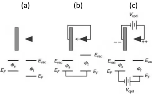
Before considering details of microscopic methods, it is important to understand the principles of electronic energy levels at the heart of electrostatic force microscopy (EFM) and Kelvin-probe force microscopy (KFM or KPFM; also SKPM is used, for scanning Kelvin-probe microscopy). Figure 2.5 depicts an idealized tip-sample system (ignoring the possible effects of a cantilever). If we bring together two dissimilar metallic materials (tip and sample) that are not electrically grounded, their electronic vacuum (energy) levels become the same (Figure 2.5 (a)). In general, the two Fermi energy levels (the highest energy of occupied electronic states) are different. If tip and sample are metallic, the difference of vacuum to Fermi level is the work function. Upon electrically connecting the
materials and assuming an adequate number of moving electrons, a substantial displacement of electron charge will act to align Fermi levels and offset vacuum levels (Figure 2.5 (b)).
This produces an electric field between tip and sample and thus a net force of attraction between opposite charges, as well as charge-dipole attractive forces[20].
Applying an appropriate external bias between tip and sample can generate a larger total tip-sample voltage difference, enhancing the strength of attraction and its possible variation from point to point along the surface (e.g., if heterogeneous in dielectric constant). This additional external bias may be needed to generate adequate image contrast EFM.2 Alternatively, by connecting just the right dc
voltage offset between the two materials, the vacuum levels can be brought into alignment and thus the force eliminated or nulled. To achieve this condition the applied voltage must be equal and opposite to the surface potential difference of the (commonly grounded) materials, also know as the contact potential (or contact potential difference, Vcpd). If the work function of the tip ϕt is greater than
that of the sample ϕs, then a positive tip voltage would be needed in order to drop the energy levels (of
negatively charged electrons) to achieve the nulling state (Figure 2.5 (c)). In KFM, one wishes to map this applied voltage across the surface to obtain a contact potential image.
Figure 2.5: idealized tip and sample electronic energies at the vacuum level and Fermi level, for the case of dissimilar work function. Materials that are (a) not electrically grounded, (b) electrically grounded (common),
and (c) electrically connected with a battery in between, of the exact potential difference needed to match the work-function difference and thus align vacuum levels.
2One should bear in mind that large biases, of order several volts, can change the electron energetics in the sample such that the method
cannot be considered a “weakly perturbative” probe of sample properties. In physicists’ language, perturbation or linear response theory does not apply, that is, the Hamiltonian of the system is being substantially modified by the strong electric field.
Figure 2.6: Block diagram of KPFM mode AFM system.
In order to realize a scanning technique which is sentitive to the surface potential the following approach is pursued: an AC voltage (VAC) plus a DC voltage (VDC) is applied to the AFM tip. VAC
generates oscillating electrical forces between the AFM tip and sample surface, and VDC is then
adjusted in a feedback cycle to nullify the oscillating electrical forces that originated from CPD between tip and sample surface. In detail the electrostatic force (Fes) between the AFM tip and sample is given by:
𝐹!" =
1 2∆𝑉!
𝑑𝐶(𝑧)
𝑑𝑧 (2.6)
where z is the direction normal to the sample surface, ΔV is the potential difference between VCPD and
the voltage applied to the AFM tip, and dC/dz is the gradient of the capacitance between tip and sample surface. When VAC sin(ωt) + VDC is applied to the AFM tip, the voltage difference ΔV will be:
𝛥𝑉 = 𝑉!"#± 𝑉!"#= 𝑉!"± 𝑉!"# + 𝑉!"sin (𝜔𝑡) (2.7)
Note that the ± sign depends whether the bias (VDC) is applied to the sample (+) or the tip (−). Substituting equation (2.7) in equation (2.6) gives the expression of the electrostatic force applied to the AFM tip:
𝐹!"(𝑧, 𝑡) = −
1 2
𝜕𝐶(𝑧)
𝜕𝑧 𝑉!"± 𝑉!"# + 𝑉!"sin (𝜔𝑡) ! (2.8)
This equation can be divided into three parts following basic trigonometric identity 𝑠𝑖𝑛!𝑥 =!!!"#!!
! : 𝐹!"= − 𝜕𝐶(𝑧) 𝜕𝑧 1 2 𝑉!"± 𝑉!"# ! (2.9) 𝐹!= − 𝜕𝐶 𝑧 𝜕𝑧 𝑉!"± 𝑉!"# 𝑉!"sin (𝜔𝑡) (2.10) 𝐹!! =𝜕𝐶(𝑧) 𝜕𝑧 1 4𝑉!" ! cos 2𝜔𝑡 − 1 (2.11)
FDC (Equation (2.9)) results in a static deflection of the AFM tip. Fω with frequency ω (Equation
(2.10)) is used to measure the VCPD, and F2ω (Equation (2.11)) can be used for capacitance
microscopy.
When electrostatic forces are applied to the tip by VAC with VDC , additional oscillating components
(due to the electrical force) will be superimposed to the mechanical oscillation of the AFM tip. A lock-in amplifier is employed to measure the VCPD, to extract the electrical force component with
frequency ω (Fω), a function of VCPD and VAC. The output signal of the lock-in amplifier is directly
proportional to the difference between VCPD and VDC. The VCPD value can be measured by applying
VDC to the AFM tip, such that the output signal of the lock-in amplifier is nullified and Fω equals zero.
Subsequently, the value of VDC is acquired for each point on the sample surface, composing a map of
the work function or surface potential of the whole sample surface area.
KPFM measures topography concurrently with VCPD, using an AFM tip. A method to separate the
topographical signal from the VCPD measurement is required.
SKPM exploits the non-contact regime of probe-sample interaction and allows to map the sample topography and surface potential in concomitantly. To stabilize performance in the attractive regime, the cantilever is driven at a frequency alightly larger than the fundamental resonant frequency, and the set point amplitude is about 90% of the free amplitude. In this way the wear of the tip is minimized and a single cantilever is used for the full characterization of a sample at various strain values.
To probe the electrostatic forces, an AC bias of 1V amplitude at a frequency 17kHz was applied to the tip. The resulting tip oscillation is fed after lock-in amplification into a feedback loop which is
engaged to null the electrostatic interaction by adjusting a DC voltage offset applied to the tip. The resulting DC-voltage called surface potential VCPD in the following, is recorded with the image
3 Materials and Methods
Device models provide a common language for the discussion of the characteristics of transistor devices. The parameters measured in device characterization are the raw material with which the behavior of devices can be summarized using a few parameters and insights about the physical processes, which underlie OFET behavior, can be explained.
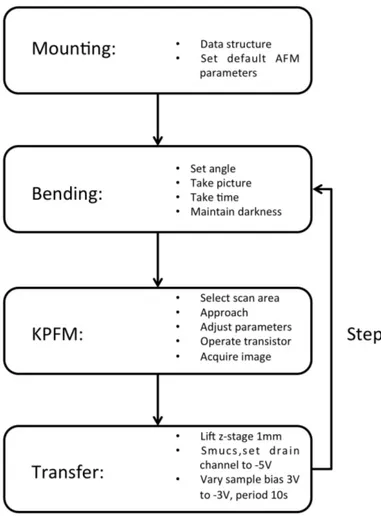
This chapter will highlight the typical TFT structure used in this experimental work (section 3.1). in section 3.2 techniques that allows to extrapolate the parameters for the transistor characterization will be described. Subsequently, in subsection 3.4, the way with which the device has been bent is presented. This includes also a description of the simulation technique applied to model the deformation in the ideal bended system. In section 3.4 the measurement KPFM setup and the choice of the parameters used are described. Methods for image analysis and image correction are detailed in section 3.5. Section 3.6 will describe the overall experimental protocol used for a complete bending experiment.
3.1 TFT structures
All OTFTs were fabrictated at
Department of Electric and Electronic Engineering, University of
Cagliari, Piazza d’Armi, Italy by Stefano Lai, Piero Cosseddu and Analisa Bonfiglio.
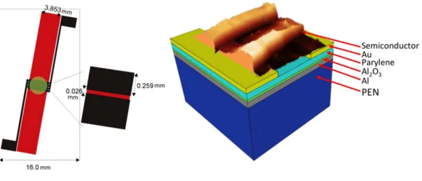
In the process, the aluminum gate electrode was deposited through a shadow-mask on a 150 um thick film of 150µm thick Polyethylenenaphtalene (PEN) as substrate to result in 90 nm thickness. The ~6 nm thick film of Al2O3 layer is realized at room temperature by UV-ozone oxidation (using a mercury lamp, UVP PenRay) performed in ambient conditions for a maximum time of 1 h. 170 nm of Parylene C are deposited by chemical vapor deposition (CVD) (Specialty Coating Systems) at room temperature, using A174 as adhesion promoter. The specific capacitance of the dielectric was determined to be 16 nF/cm2. Thermally evaporated gold source and drain contacts (40 nm thickness) are realized on top of the Par C layer with a photolithographic process. The channel defined by these interdigitated electrodes amounts to length and width of L=26 µm and W = 23.12 mm, respectively.6,13-Bis(triisopropylsilyle-thynyl)pentacene (TIPS) was deposited by drop casting from a 1% solution using anisole as organic solvent. Poly(3-hexyl-thiophene) was deposited by dropcasting from a solution of 1% in chlorobenzene. The cross section of the described device is shown in Figure 3.1 (b).
Figure 3.1: (a) top view of typical TFT used in these experiments. (b) The cross section of the TFT shows the amount and types of different layers used. Scale is not respected.
3.2 Transistor Characterization
Besides its technological interest, the thin-film transistor is also a tool of choice to analyze charge injection and transport in organic semiconductors. In that respect, methods for extracting the basic parameters are of crucial importance. Equations (1.13) and (1.14) are the premise for the most popular methods for mobility extraction[11].
The probably most widespread one makes use of the transfer characteristic in the saturation regime, and this is the regime in which we conducted experiments.
A Keysight B2912A sourcemeter, was used to provide the VDS potential and measure the drain current
ID. VG potential is set by the AFM electronics and is applied to the sample holder of the instrument
and further wired to the Al-gate electrode. The transfer characteristic was taken in saturation regime, at VDS=-5V while VG potential is swept from -3V to 3V for a period of 10 seconds. The output
characteristic was taken varying VD from 0V to -5V with steps of ΔVD=0.1V and varying VG from 2V
to -5V with steps of ΔVG=1V.The Smucs software created by Dr. Tobias Cramer, researcher in the
University of Bologna, acquired all the data.
All relevant parameters like mobility and threshold voltage were calculated from these acquired data with the formula described in
(3.1). In practise these parameters were extrapolated from the linear fit of 𝐼! versus VG graph
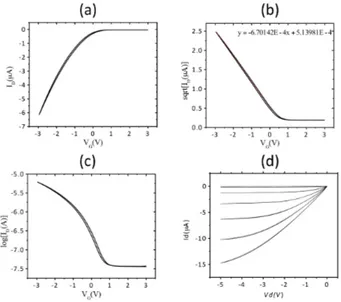
(example in Figure 3.2 (b)).
More precisely, the square root of the drain current is plotted as a function of the gate voltage. The principle of the method can be illustrated by rewriting equation (1.14) as
𝐼!"#$ =
𝑊
2𝐿𝐶!𝜇 𝑉!− 𝑉! (3.1)
(3.1) predicts a straight line; the mobility is obtained from the slope of the line, while the threshold voltage corresponds to the extrapolation of the line to zero current.
However, this method presents a critical drawback. In the saturation regime, the density of charge varies considerably along the conducting channel, from a maximum near the source to practically zero at the drain. As will be seen in the following, the mobility in organic semiconductors is not constant; rather, it largely depends on various parameters, including the density of charge carriers. A direct consequence of this is that in the saturation regime, the mobility is not constant along the channel, and the extracted value only represents a mean value and instead of a straight line a curvature is observed at voltages close to threshold. For this reason, I select a rage of higher Vg-values where (3.1) is valid and I can consider µ constant, so I’m interested in the part of curve where the slope is constant.
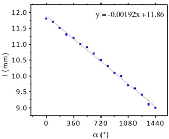
Figure 3.2: Representative transfer (a)(c) and output characteristic output (d) of organic transistor. The fit in (b) is is used for calculate the mobility µ and the threshold voltage VTH.
The off current IOFF was determined using the graph Log(ID) versus VG. IOFF current was calculated by
the mean value in the pinch-off condition), in the 1.5V<VG<2.5V range.
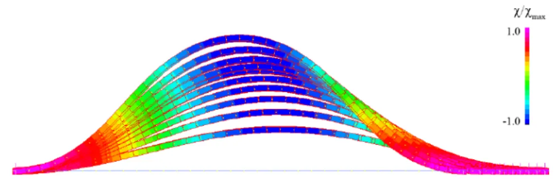
3.3 Deformation of TFT
One key advantage of organic electronic devices is the possibility to produce flexible all-organic OTFTs with the functional organic semiconductor films deposited on flexible plastic foils like Mylar or Polyethylenenaphtalene (PEN, which has been studied in this chapter) as substrate.