UNIVERSITÀ DEGLI STUDI DI PISA
Facoltà di Ingegneria
Corso di Laurea in Ingegneria Elettronica
Tesi di Laurea Specialistica:
SVILUPPO DEL NUOVO SEQUENCER E DELLA
NUOVA MEMORIA ASSOCIATIVA DEL SILICON
VERTEX TRACKER DELL’ESPERIMENTO CDF
Relatori:
Prof. Giuseppe Iannaccone
Candidato:
Massimiliano Bitossi
Prof. Mauro Dell’Orso
Anno Accademico 2004-2005
1.1-3
Introduction
During my thesis I have collaborated at the Silicon Vertex Tracker (SVT) [1] upgrade, a processor, that belongs to the CDF [2] experiment, situated in Batavia, in the state of Illinois, USA. CDF is an international collaboration and the National Institute of Nuclear Physic (INFN) of Pisa is part of it. This thesis has been developed in this Institute. The work that is reported in this thesis concerns the development and the validation of part of the SVT device.
The CDF experiment is a powerful particle detector, devoted to studies of high energy physics phenomena. These particles are generated by p-pbar collisions, produced by the Tevatron Collider at Fermilab [3], that is the accelerator with the most high energy available today. The modern detectors produce an enormous amount of data that have to be processed in real time. One of the most difficult tasks during the on-line data elaboration is the track finding problem, that in the case of a p-pbar experiment is very complex. In the CDF experiment the solution is entrusted to the SVT device, that is a dedicated processor. SVT is a fundamental part of the trigger system, devoted to the selection of events that deserve to be written on tape.
The SVT is specialized in the complex operation of pattern recognition in very crowded events (a lot of trajectories that intersect the detector’s layers), produced at very high rate (50KHz). All the interesting trajectories are memorized in the Associative Memory (AM) [4]. The SVT’s purpose is to receive the data from the detector and to load them to the AM that extracts the trajectories that are compatible with the event. A trajectory is compatible with an event if the right channel for each layer, the one that correspond to the trajectory, is fired and the corresponding “hit” (channel coordinate) is included in the event data. So it is possible to use a modular structure where each module contains a pattern corresponding to an interesting trajectory. It is important to highlight that the number of patterns for silicon detectors can be very large, if the detector has a very good resolution. A possible compromise is obtained operating with a resolution that is worse than the detector’s resolution. Patterns are calculated using superstrips (SS), that are the logic OR of contiguous channels, instead of single channels. In this thesis I call “hits” the addresses of the detector’s fired superstrips and “roads” the rough found trajectories. Each road contains an array of superstrips for each layer of the detector [5]. Each road can contain more than a single real track and also fake tracks. Each combination of
1.1-4
hits contained in the road is fitted with the full detector resolution to select real tracks and reject the fakes one.
The CDF experiment aims to discover new particles that validate or reject existing physic models. For this purpose the performances of the detector and the accelerator have been continuously expanded. As luminosity rises, the chance to discover rare particles increases, but multiple interactions make more difficult the good event selection. The number of hits in the detector (occupancy) increases. Thus the time to process the events increases. For SVT the more serious problem is the increase in the number of found roads and track candidates that have to be fit. In each road, the number of fits that has to be done is the combinatory due to multiple hits in each layer. As the hit density in the detector increases, the number of fits can become quite large. So an upgrade of the SVT device has been demonstrated to be necessary. The SVT upgrade aims to both reduce the number of fits and to perform each fit more quickly. The former is done by reducing the width of roads by increasing the total number of roads. The latter is achieved by increasing the speed of the track fitting board.
The INFN of Pisa has the task to develop and test two boards that are a fundamental part of the new SVT device. The most important board is the Associative Memory board (AM++ with its plug-in LAMB++) that allows an increase of the total associative memory of a factor 40 with respect the old one. The second board is the AM++ controller, the Associative Memory Sequencer that also collect the Road Warrior function on the same board (AMS-RW). The Road Warrior removes redundant track candidates prior to track fitting.
These boards are allocated in a VME [6] crate with other service boards.
The AMS-RW is implemented on a Pulsar board [7], a general-purpose, powerful board. The Pulsar design, based on large interconnected FPGAs, is very flexible. The use of four mezzanine cards allows various input and output protocols or the use of large on-board RAMs. The large increase in the number of roads is achieved with a new AM chip produced [8] with Standard Cell technology This thesis reports the work about the development and the validation of the AM++ and Pulsar’s firmware .
The system composed of these two boards “AMS-RW & AM++” represents the SVT core. The AMS-RW and the AM++ perform the operation of patterns recognition. Another argument of this thesis is the construction of the test stand and of test tools to validate the system.
1.1-5 This thesis has the following structure:
• In the chapter 1 the CDF experiment is introduced and the role of the SVT device is explained. Each board that is part of the SVT device is highlighted and its architecture is explained focalizing the attention on the AMS-RW, AM++ with its plug-in LAMB++ boards, object of my thesis. Moreover a short introduction of the Boundary Scan tools is reported.
• In the chapter 2 I describe all the work that concerns the diagnostic of the two boards. In particular is explained the development of the test tools to globally check and simulate the data taking and check the connections of all the boards. Moreover I describe my work to include diagnostic tools inside the logic architecture of the chips placed on the AM++ and LAMB++.
• In the chapter 3 the Pulsar board is introduced and its architecture is described. It is shown how it is possible to use the Pulsar to realize the AMS-RW. The chapter reports all the work on the VHDL firmware. Moreover the internal test tool of the SVT (Spy Buffers and Error Flags) development is described.
• In the Appendix A the details of the program used in the thesis are reported.
• In the Appendix B the Boundary Description language and its use in my thesis is described.
1.1-7
Contents:
Chapter 1 Upgrade of the Silicon Vertex Trigger...1.1-10 1.1 The CDF detector ...1.1-10 1.1.1 The CDF trigger system ...1.1-14 1.2 Introduction to the SVT device ...1.2-14 1.3 SVT protocol ...1.3-16 1.3.1 Packets and Events ...1.3-17 1.3.2 Hit and Road Data ...1.3-19 1.4 The Upgrade of SVT ...1.4-20 1.5 The Merger ...1.5-22 1.6 The AM++...1.6-22 1.7 LAMB++...1.7-24 1.8 The AMchip ...1.8-25 1.9 The AMS-RW ...1.9-25 1.10 The Boundary Scan ...1.10-27 1.10.1 The Instruction Register (IR) ...1.10-28 1.10.2 Tap Controller ...1.10-32 1.10.3 The Boundary Scan Path ...1.10-34 Chapter 2 The diagnostic of the boards ...1.10-37 2.1 Introduction ...2.1-37 2.2 The Test Stand and the Random Test...2.2-38 2.3 The global test of the system...2.3-41 2.4 The AMS-RW Spy Buffers and Error Flags ...2.4-43 2.5 The specific-board test tools ...2.5-44 2.5.1 The specific tests on the AMS-RW...2.5-46 2.5.2 The specific tests on the AM++ and its plug-in LAMB++ ...2.5-46 2.5.3 The Input Control chip ...2.5-49 2.5.4 The VME chip...2.5-51 2.5.5 The Bousca chip ...2.5-59 2.5.6 The Software ...2.5-60 2.5.7 The AM_input_test.c program ...2.5-61 2.5.8 The sample.c program ...2.5-62 Chapter 3 The AMS-RW board ...2.5-67 3.1 Introduction ...3.1-67 3.2 The Pulsar board...3.2-67 3.3 The Associative Memory Sequencer-Road Warrior (AMS-RW) ...3.3-72 3.4 The firmware and the implementation of the AMS-RW in the Pulsar Board...3.4-76 3.5 DataIO2 FPGA ...3.5-78 3.6 CONTROL FPGA...3.6-78 3.7 DATAIO1 FPGA ...3.7-80 3.8 The Finite State Machine of the CONTROL FPGA ...3.8-82 3.9 The End Event Word and the Error Flags ...3.9-82 3.9.1 The Parity Error...3.9-84 3.9.2 The Output Parity ...3.9-85 3.9.3 The Truncated Output ...3.9-85
1.1-8
3.10 The Spy Buffers ...3.10-86 3.10.1 Spy Buffer Implementation...3.10-87 APPENDIX A ...3.10-92 The pattgen.c program...3.10-92 The writepatterns.c program ...3.10-93 The genhits.c program...3.10-94 The AMsim.c program ...3.10-96 The MGRrun.py program...3.10-97 The road_diff.c program ...3.10-97 The CHANGEME.h program ...3.10-98 APPENDIX B ...3.10-100 Figure 1.2.1 ...1.2-16 Table 1.3.1...1.3-19 Table 1.3.2...1.3-20 Table 1.4.1...1.4-20 Figure 1.4.2 ...1.4-21 Figure 1.6.1 ...1.6-23 Figure 1.6.2 ...1.6-24 Figure 1.9.1 ...1.9-26 Figure 1.10.1 ...1.10-29 Figure 1.10.2 ...1.10-30 Figure 1.10.3 ...1.10-32 Figure 1.10.4 ...1.10-35 Figure 1.10.5 ...1.10-36 Figure 2.2.1 ...2.2-39 Figure 2.2.2 ...2.2-39 Figure 2.2.3 ...2.2-40 Figure 2.2.4 ...2.2-41 Figure 2.3.1 ...2.3-43 Figure 2.5.1 ...2.5-47 Figure 2.5.2 ...2.5-50 Table 2.5.3...2.5-54 Table 2.5.4...2.5-55 Table 2.5.5...2.5-55 Figure 2.5.6 ...2.5-56 Table 2.5.7...2.5-57 Table 2.5.8...2.5-57 Figure 2.5.9 ...2.5-59 Figure 2.5.10 ...2.5-64 Figure 2.5.11 ...2.5-65 Figure 3.2.1 ...3.2-69 Figure 3.2.2 ...3.2-71 Figure 3.2.3 ...3.2-71 Figure 3.3.1 ...3.3-72 Figure 3.3.2 ...3.3-74 Figure 3.6.1 ...3.6-79 Figure 3.6.2 ...3.6-80 Figure 3.7.1 ...3.7-81
1.1-9 Figure 3.10.1 ...3.10-92 Figure 0.1 ...3.10-95 Table 0.1...3.10-97 Figure 0.1 ...3.10-99 Figure 0.1 ...3.10-101 Figure 0.2 ...3.10-101 Figure 0.3 ...3.10-101 Figure 0.4 ...3.10-102 Figure 0.5 ...3.10-102 Figure 0.6 ...3.10-104
Chapter 1
Upgrade of the Silicon Vertex Trigger
This chapter introduces the CDF experiment and the Silicon Vertex Trigger (SVT) device. The existing and upgraded SVTs are described. In particular I report about the two boards that have been object of my thesis work: the AMS-RW and AM++ boards. The Boundary Scan (BS) [9] is also described since I use it for board tests.1.1 The CDF detector
In this paragraph I give an overview of the Collider Detector at Fermilab (CDF) [10], that it placed on the Tevatron Collider [i] at Batavia in Illinois (USA).
Figure 1.1.1
An isometric view of the CDF II detector.
Figure 1.1.1 shows an isometric view of the CDF II detector. The inner part of the detector is the tracking system which is contained in a superconducting solenoid providing a magnetic field of 1.4 Tesla. Outside the solenoid there is the calorimeter system, which provides energy
1.1-10
i
The Tevatron Collider is the accelerator where the p-pbar collisions are produced with the maximum energy ever seen in the word (2Tev).
measurements for electrons, photons [ii] and jets [iii]. The calorimeters are contained into a shell of steel absorbers that shield the muon [iv] chambers, the outermost part of the CDF detector, from non-muon particles generated by proton-antiproton interactions. I describes the tracking detectors only. A complete description of the CDF detector can be found in [11].
Figure 1.1.2
This is a longitudinal section of one quadrant of the CDF tracking systems.
Figure 1.1.2 shows one quadrant of the longitudinal section of the CDF tracking system. The outermost detector is the Central Outer Tracker (COT) drift chamber. The COT provides full coverage for η <1 [v], with an excellent curvature resolution [vi]. The COT is the core of the
ii
Electrons and photons are particles commonly observed in events generated by the p-pbar collisions.
iii
Jets are groups of particles, very near in the detector so that they can be observed as a single entity.
iv
Muons are particular particles able to cross the calorimeter without being stopped. Muons are detected by the chambers outside the calorimeter.
v
2 ln θ
η = tag is called pseudo-rapidity, θis the polar angle, related to the proton – antiproton beam. θ =0
means the beam’s axis.
1.1-11
vi
Particles are bended in the transverse plane to the beam by the magnetic field generated by the solenoid. The measure of the trajectory curvature provides information on the transverse momentum.
integrated CDF tracking system. The COT provides 3-dimensional track reconstruction with 96 detector layers. The 96 layers are organized into 8 super-layers. Four of which are axial, while the others, called stereo, are at small angles. Inside the COT there are the silicon detectors: SVX II [12], ISL [13] and L00 [14]. They are complementary to the COT. They provide an excellent transverse impact parameter [vii] resolution of27µm. The silicon detectors provide 3-dimensional track reconstruction. The achieved longitudinal impact parameter resolution is70µm. Figure 1.1.3 shows a cross section of the SVX II. The SVX II is organized into 12 azimuthal wedges. For each wedge there are 5 detector layers each providing one axial measurement on the other face.
Figure 1.1.3
Cross section of the SVX II detector.
1.1-12
vii
Figure 1.1.4 shows an isometric view of the SVX II. The SVX II is made of three mechanical barrels. Each mechanical barrel is made of two electrical barrels. In fact, within a mechanical barrel each detector element is built of two silicon sensors with independent readout paths. The two sensors are aligned longitudinally to achieve a total length of 29cm, which is the length of each mechanical barrel. Hence, for each wedge and for each layer there are a total of 6 sensors belonging to 3 different mechanical barrels. The L00 and ISL silicon detectors complete the silicon subsystems. The L00 detector, which is directly mounted on the beam pipe, provides best impact parameter resolution. The ISL detector provides up to two additional tracking layers, depending on track pseudo-rapidity, that allow standalone silicon tracking.
In particular, ISL allows to extend tracking beyond the COT limit(η <1), and up to
) 2
(η < . The L00 and ISL detectors are not used by the SVT.
Figure 1.1.4
Isometric view of the SVX II detector.
1.1.1 The CDF trigger system
The trigger system selects about 10 events/s to be written on tape between the
events/s produced by p-pbar collisions. To perform this terrific task efficiently the trigger system is organized into three levels.
6 10 * 6 . 7
The first trigger level is organized as a synchronous pipeline that processes events at the bunch crossing rate (7.6Mhz) and takes trigger decisions within a latency of 5.5µs. The second trigger level processes events selected by the level-1 (20Khz) within a nominal latency of 20µs.
The third trigger level is made of a large CPU farm, which run off-line reconstruction code. A detailed description of the CDF trigger system can be found in [15].
The structure of both level-1 and level-2 is similar and is based on a dedicated hardware. Physical objects are reconstructed by the sub-processors, which fed data to the global decision hardware that combines this information and takes the trigger decision.
1.2 Introduction to the SVT device
The CDF experiment used a fast on-line track processor since the begin of Run I [16]. It was able to reconstruct tracks at low spatial resolution in the drift chamber down to a Pt [viii] threshold of 2.5GeV in an average time of 2.5µs. This was a crucial tool used to keep under control the muon and electron trigger rates.
After an upgrade period the CDF II [17] experiment is running. It uses two track processors called XFT [18] and SVT [19].
XFT [ix] reconstructs tracks in the drift chamber down to a Pt threshold of 1.5GeV. The XFT is pipelined and reports the results for a new event every 396ns, with a typical latency of 2µs. It is suitable for Level-1 trigger [x], [20] decision.
viii
The trasversal impulse, related to the beam’s axis, is called shortly Pt . It is the impulse computed in the trasversal
plane to the beam.
1.2-14
ix
The CDF II experiment introduced a second track processor called SVT [xi]. SVT reconstructs tracks in the silicon detector within 20µs using the full silicon resolution and providing a measurement of transverse impact parameter with spatial resolution comparable to that of the off-line. It is used for the Level-2 trigger [21] decision. Thanks to the SVT processor, the CDF II experiment was the first one to reconstruct secondary vertices characterized by a small distance )(100µm from the primary vertex generated by the p-pbar collision. The detection of the secondary vertex is the fundamental signature of a b-quark decay ( the b-quark decays after a very short life, corresponding to a travel distance of few 100µm). For the first time we could observe fully hadronic decays of the bottom quark at a hadron collider.
Now we are working for an upgrade of the SVT device but before presenting the SVT upgrade, we review the existing device. SVT is divided into 12 independent processors, one for each silicon detector wedge. A sketch for one processor working for one of the 12 azimuthal wedges is shown in Figure 1.2.1. Raw silicon hits are transmitted on optical fibers to Hit Finder boards that find hit clusters in each silicon layer and calculate their centroids. The Merger board then combines the silicon data from 3 Hit Finders with the drift chamber tracks found in that wedge. The combined information is sent to both the Associative Memory system [22], which does the pattern recognition, and a Hit Buffer [23] which stores the hits until a pattern is found with sufficient hits to be deemed a track candidate. There are three pattern recognition boards, a Sequencer that controls the operation and two Associative Memory (AM) boards that find track candidates. The Sequencer converts silicon hit coordinates into coarser resolution superstrips, typically 500 µm wide, a resolution appropriate for pattern recognition. The AM boards contain AM chips which are content addressable memory. There are 32K patterns stored, each containing the superstrip (SS) number for a drift chamber track and for each silicon layer. As each hit passes through the AM boards, all patterns see it at the same time. If the SS number is the same as the one stored in the pattern for that layer, then the layer is marked as on. When all silicon and drift chamber data have passed through the system, each of the 32K patterns has a word containing the layers that were hit. Majority logic selects those patterns (“roads” in the figure) with a drift chamber track and the requisite number of silicon hits and passes them to the Hit Buffer board.
As each road enters the Hit Buffer, the silicon hits are retrieved at full resolution and passed to the Track Fitter along with the road number. Because the roads are quite narrow, each one
x
The trigger decision.
1.2-15
xi
corresponds to an approximate track momentum, azimuth, and impact parameter. This permits track fitting to be done with the requisite resolution using a linear approximation. The 6 inputs (4 silicon hits plus the drift chamber track azimuth and curvature) are used to produce 6 outputs (impact parameter, improved curvature and azimuth, plus 3 constraints that are combined into a fit ). Tracks that pass a cut are sent to the Ghostbuster board. If there is more than one silicon track associated with a single drift chamber track, the Ghostbuster selects the one with the smallest . Also shown in the figure is the recently added Road Warrior, a Pulsar board that removes duplicate track candidates prior to fitting.
2
χ χ2
2
χ
Figure 1.2.1
The SVT boards for one of 12 azimuthal wedges.
1.3 SVT protocol
Data flow in and out the SVT boards as data streams. Each stream enters or leaves an SVT board through a dedicated connector and cable.
A uniform communication protocol is used for all data transfers throughout the SVT system. Data flow through unidirectional links connecting one source to one destination. The protocol is a simple pipeline transfer driven by an asynchronous Data Strobe (DS_ in the following text, it is an active low signal). To maximize speed, no handshake is implemented on a word by word basis. A Hold_ signal is used instead as a loose handshake to prevent loss of data when the destination is busy (it is an active low signal and will be called HOLD_ in the following text). Data words are sent on the cable by the source and are strobed in the destination at every
1.3-17
positive going DS_ edge. The DS_ is driven asynchronously by the source. Correct DS_ timing must be guaranteed by the source. Input data are pushed into a FIFO buffer. The FIFO provides an Almost Full signal that is sent back to the source on the HOLD_ line. The FIFO is popped by whatever processor sits in the destination device. If the destination processor does not keep up with the incoming data rate, the FIFO becomes Almost Full and the HOLD_ signal is sent to the source. The source responds to the HOLD_ signal by suspending the data flow. Using Almost
Full instead of Full gives the source plenty of time to stop (the equivalent of 127 DS_ cycles).
The source is not required to wait for an acknowledge from the destination device before sending the following data word, allowing the maximum data transfer rate compatible with the cable bandwidth even when transit times are long. Signals are sent over flat cable as differential TTL. The maximum DS_ frequency is what is allowed by the Pulsar input FIFOs, and is roughly 40, 50 MHz.
Here we describe the connections and formats of data flowing in SVT during data taking. A second important connection is the one necessary for the SVT board control, monitoring and downloading. This is done from computers that are connected to the SVT system using the VME standard [24]. All SVT boards are VME slaves.
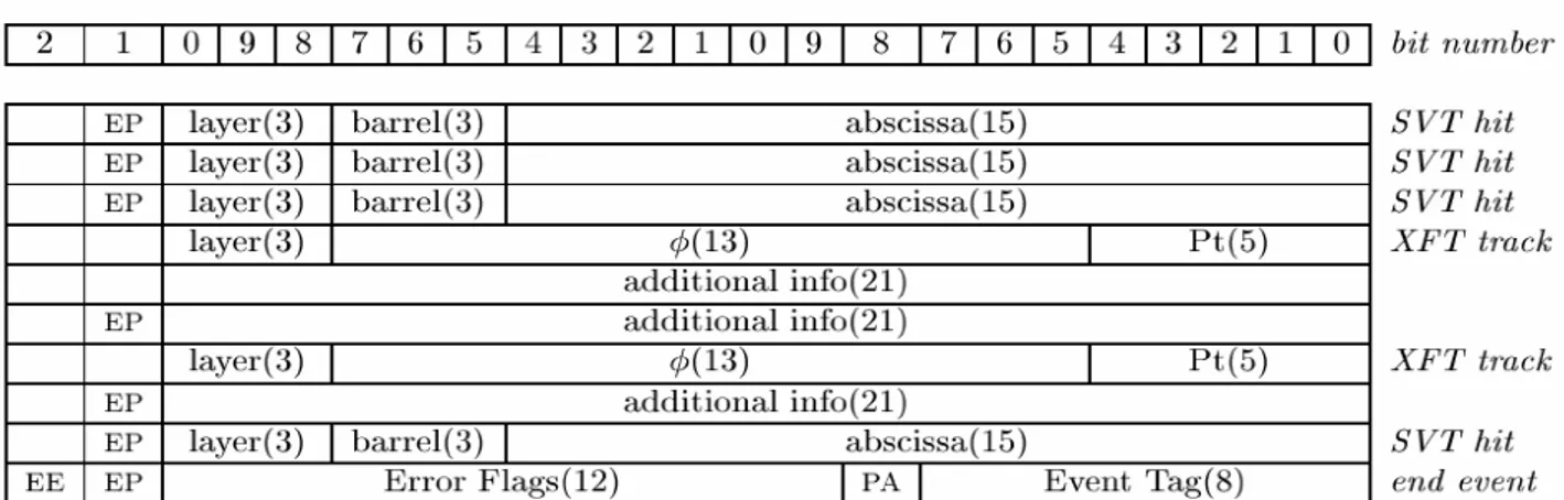
1.3.1 Packets and Events
On each cable there are 21 data bits, Data Strobe (DS_), HOLD_, End Packet (EP), End
Event (EE), for a total of 25 signals (50 wires). Data are sent as packets of words. The first
word of each packet is called head. In the simplest case a packet may consist of a single word,
the head, otherwise, if more than 21 bits are needed, a packet may consist of two or more
words. The words following the head, in a multi-word packet, are collectively called body. The EP bit marks the last word of each packet, the End Packet word. In one-word packets, of course, the word has EP = 1.
The EE bit is used to mark the end of the data stream for the current event. The complete sequence of words in a data stream is called an Event. Each board will assert EE on the output stream after it has received an EE in each input stream and has no more data to output. The last word of each Event, the End Event word, has a special format. It has EE = 1 and EP = 1. The data field in the End Event word is used for Event Tag (8 bits), Parity (1 bits), and Error Flags (12 bits), as shown below.
1.3-18 DATA fields in the End Event Word
Bit range 20-9 8 7-0
1.3.2 Hit and Road Data
In the hit stream, driven by the Hit Finders and the COT Track Finder (see Figure 1.4.2), each packet is called a hit. Each word contains a hit coordinate in the data field (21 bits). Hits may be one word long or more depending on what kind of detector the hit is coming from (SVX or XFT). The Layer number (3 MSB) is contained only in the packet head. XFT hits are also called tracks.
In the road stream, driven by the Associative Memory, each packet is called a road. All roads were one word in length. The 21 bits of the data field were the road number. With the SVT upgrade a second word has been added to each road packet, the “bitmap”. It is a 6 bits word, one bit per layer. Each bit says if the corresponding layer was fired (bit = 1) or not fired (bit = 0). In
Table 1.3.1 and Table 1.3.2 the Hit and road formats are shown.
Table 1.3.1
The table shows the hit format sent to the AM++ and Hit Buffer by the Merger.
Table 1.3.2
The table shows the output road format sent to the Hit Buffer by the AM++.
1.4 The Upgrade of SVT
As luminosity rises, multiple interactions increase the number of hits in the SVX. Thus the time to process all of the silicon hits increases (time/hit = ~35 ns). However the more serious problem is the increase in the number of track candidates that have to be fit (time/fit = ~300 ns). In each road, the number of fits that has to be done is the product of the number of hits in each silicon layer. As the hit density in the silicon increases, the number of fits can become quite large.
The SVT upgrade aims to both reduce the number of fits and to perform each fit more quickly. The former is done by reducing the width of roads by increasing the total number of roads per wedge from 32K to 512K. The latter is achieved by increasing the speed of the track fitting board.
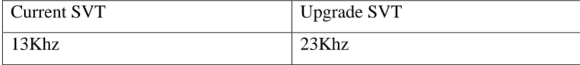
Table 1.4.1 shows the improved SVT performance with these upgrades. The increase in the amount of data SVT can process is very significant.
Current SVT Upgrade SVT
13Khz 23Khz
Table 1.4.1
The maximum SVT input rate at 3*1032 luminosity so that the dead-time does not exceed the 5%. 1.4-20
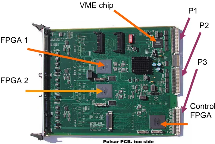
The SVT upgrade is designed to require a minimum of new hardware. The increase in the number of roads is achieved with a new AM system, the AM++. New prototype AM chips have been produced. The new Sequencer uses a Pulsar board [25], which was designed for and is now being used in the CDF level-2 upgrade. The Pulsar design is very flexible, with mezzanine cards for various input and output protocols and three powerful FPGAs for data manipulation. A simple mezzanine card containing memory chips and firmware for the Pulsar FPGAs are the major needs for the AM Sequencer. The AM Sequencer will also carry out the Road Warrior function, to remove redundant track candidates prior to track fitting.
The existing Hit Buffer cannot be used with the proposed increase in the number of track patterns. The Hit Buffer functionality will be transferred to a Pulsar board. The additional needed memory will be located on a mezzanine card.
The new Track Fitter also use the Pulsar board, taking advantage of its factor of 3 higher clock speed compared to the current Track Fitter. A mezzanine card similar to those used on the other SVT Pulsar boards will be utilized here. The FPGA firmware is based on the firmware in the current Track Fitter.
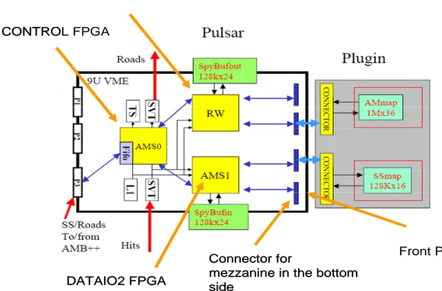
The block diagram of the upgraded SVT with the 3 Pulsar boards per wedge is shown in Figure 1.4.2. Below a short description of the boards is reported. The boards that are object of my thesis are AM++ , with its plug-in LAMB++ and the AMS-RW.
Figure 1.4.2
The Block diagram of the upgraded SVT.
1.6-22
1.5 The Merger
The Merger VME board has the task to merge up to four independent data streams into a single one. The merging of the streams is performed on a “first come first serve” basis preserving the packet structure (packets cannot be split). Packets in the output stream will be a random mix of packets from the different input streams. The End Event word is asserted on the output stream after End Event is received on all input streams and all the packets have been output.
There are 4 input streams and two equal output streams. The maximum working frequency of the board is 33 MHz. An overall sketch of the MERGER board is shown in Figure 1.6.1.
Data from each of the four inputs are treated in the same way. Packets are copied from input to output with no modification (with the exception of the EE word). The MERGER does not provide any means of tagging packets to identify which stream they come from.
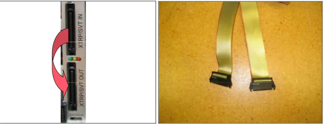
The MERGER has 6 ways of working: “Run Mode” and 4 “Tests Modes”. We use MERGER in one of the 4 Test Modes. In this mode the input channel used for hits is set so that data are not expected from the cable, but are written through VME in the spy buffers [26]. The hits are sent from the workstation connected with Ethernet to the VME CPU. This operation has low speed so firstly the hits are stored in the spy buffer on the MERGER and then they are sent at the maximum rate (33Mhz) to the AMS-RW. The roads are sent back to the Merger on the SVT cable by the AMS-RW and written on the spy buffer of this channel. The spy buffer is read through VME.
1.6 The AM++
We have designed a new Associative Memory Board (AM++) for track finding. It is a 9U VME board, compatible with the old and the new sequencer. It works at a clock frequency of 40MHz and has a modular structure, consisting of 4 smaller boards, the Local Associative Memory Banks (LAMBs). Each LAMB contains 32 Associative Memory chips, 16 on each side of the board. The AM++ board is sketched in Figure 1.6.2. The structure of the LAMB is also shown. The AM chips come in PQ208 packages and contain the stored patterns and read-out logic.
It is important to remember that in order to contain the pattern bank within an acceptable size the AM operates at a coarser resolution than the actual detector. This is usually done by clustering single contiguous detector channels into larger superstrips. In the following, we will call “hits” the addresses of fired superstrips in each layer, and “roads” the coarse resolution trajectories (each road corresponds to an array of superstrip addresses – one per detector layer). When an AM++ board starts to process an event, the hits are received by the input control chip, see Figure 1.6.2, and then they are simultaneously sent to the four LAMBs. As soon as hits are downloaded into the LAMBs, the locally found roads set the request to be read out (Data Ready). Once the event is completely read out, the LAMBs make the last matched roads available within a few clock cycles.
The outputs of the 4 LAMBs are multiplexed into a single bus by a purposely-designed TOP GLUE chip (see Figure 1.6.2) sending roads to the AM Sequencer through the P3 connector. The TOP GLUE receives from the AM Sequencer and distributes to the LAMB Glues a set of Operation Codes that define the road readout order. The majority logic available in the AM chip is driven so that roads are readout with an ordering that gives priority to the most constrained matches.
Figure 1.6.1
MERGER board overall scheme.
PAM GLUE FIFOS RECEIVERs & DRIVERs (ROAD bus + 6 HIT buses) LAMB CONNECTORs VME INTERFACE ROAD CONNE CTO R HI T CONNECT O R TOP GLUE PIPELINE REGISTERs INDI Figure 1.6.2
AM board layout. Dashed lines show areas occupied by LAMBs. On top left corner the high light area shows details of one LAMB.
1.7 LAMB++
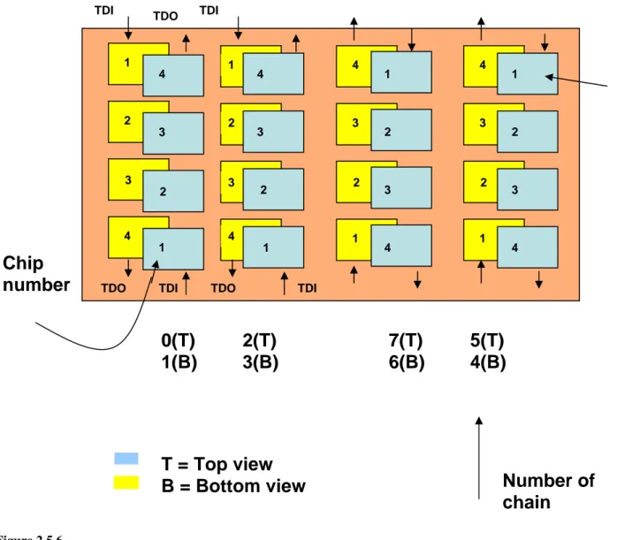
Six hit buses, one for each detector layer, are fed in parallel to the four LAMBs and distributed to the 32 AM chips on the LAMB through 12 fan-out chips called Input Distributors (INDI). For the output road address bus, the AM chips on each LAMB are divided into 4 pipelines, each corresponding to a column in Figure 1.9.1, consisting of 8 chips, 4 on the front and 4 on the back. Each AM chip receives an input bus where road addresses found in previous chips are propagated, multiplexes it with the road addresses internally found in that chip, and sends the output to the next chip. Signals propagate from one chip to another on the top and bottom PCB planes through very short pin-to-pin lines, without any vias.
The outputs of the 4 pipelines are then multiplexed into a single bus by a specially designed GLUE chip on each LAMB.
The LAMB board has been designed, optimized, simulated, placed, and routed with Cadence software. It represents a significant technological challenge due to the high density of chips allocated on both sides of the board and the use of the advanced Chip-scale packages (CSP) for the 12 INDI chips and the GLUE chip (see Figure 1.9.1).
1.9-25
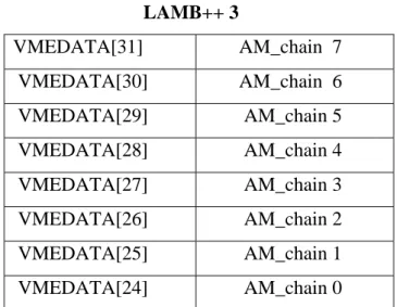
Successful operation has been tested at a clock frequency of 40MHz with the new standard cell chip. Patterns are downloaded through the VME controlled JTAG port. Chains of 4 AMchips each are downloaded in parallel to reduce programming time. The VME 32-bit wide data transfer allows us to program 32 chains in parallel for a total of 4 LAMBs. Downloading time is a few seconds.
1.8 The AMchip
The upgraded associative memories has been produced using standard cell technology to achieve the maximum pattern density without resorting to full custom design. We are using the UMC 0.18 micron technology since it is the most convenient. A 10x10 mm die contains 5000 “CDF patterns” (patterns for a six layer detector).
We used a Multi Project Chip (MPC) to get a low cost prototype. For the small number of required chips (~2000), a single pilot run of 12 wafers (3000 chips) has been done. In this case each wafer produces ~ 250 chips. The standard cell chip has been built pin compatible with an FPGA chip, so that extensive board tests have been prepared before receiving the standard cell prototype.
For the implementation of the AM chip, we have chosen a commercial low cost FPGA family (Xilinx Spartan 0.35 micron process). The FPGA approach allows a larger degree of flexibility in the prototyping and testing phase of the project. Details of the Spartan family can be found on the Xilinx web page [27].
The FPGA AM chips have been logically designed with the same VHDL code that defines the standard cell chip and have been mapped into FPGAs with Synopsis. The pattern density has been drastically reduced to 2 patterns to obtain a logically equivalent chip working at high frequency (40MHz).
1.9 The AMS-RW
The AMS-RW card implements and enhances the functions of two boards installed in the current SVT: the Associative Memory Sequencer (AMS) and the Road Warrior (RW).
The AMS will be the operating sequencer for the AM++ associative memory boards, and the RW function will eliminate redundant track candidates before track fitting.
The greatly increased number of track patterns, the protocol for the new AM chips, and the necessity of increasing processing speed require a new AMS-RW board.
The new LAMB++ 2005
AM chip
INDI
Glue chip
BOUSCA chip
Figure 1.9.1
Top view of LAMB++ board.
The plan is to use a Pulsar board [28], which is highly reconfigurable and complies with CDF and SVT standards, to implement both the AMS and RW functions. A custom mezzanine card to be plugged into the Pulsar will satisfy the memory needs of the AMS - RW algorithms.
1.10-27
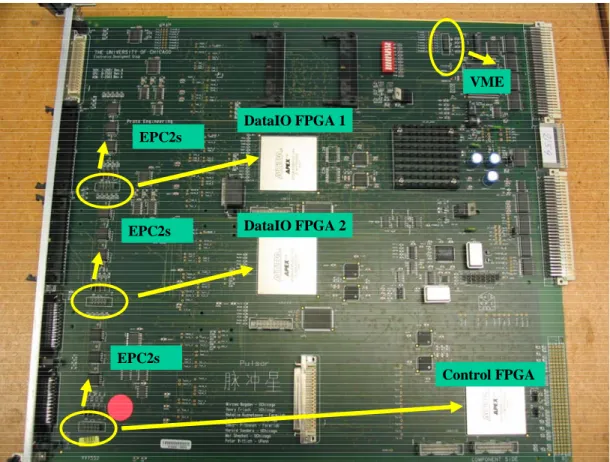
The firmware for all the necessary logic will be contained in the 3 large Altera APEX20K400-1XV FPGAs [29] on the Pulsar. I have contributed to the developing of the AMS-RW’s firmware. This work is explained in Chapter 3, where major details about the AMS-RW are reported.
1.10 The Boundary Scan
The JTAG 1149.1 IEEE Standard [30], commonly named Boundary Scan (BS), is one of the most important instruments for testing and debugging modern electronic boards. Boundary Scan provides standard and user defined function. In this chapter we describe in details our use of the BS to test input and output signals (EXTEST, SAMPLE functions) and to verify the interconnections between the chips. The chips that contain Boundary Scan can drive and register the logic levels of the I/O pins.
Instructions and data values are downloaded using an interface of only four pins, the Test Access Port (TAP): Test Data In (TDI), Test Data Out (TDO), Test Clock INPUT (TCK) and Test Mode Select (TMS).
TAP provides the possibility to access the I/O pins in serial mode, using a flow Data Register, called Boundary Scan register, shown as a chain of black squares in
Figure 1.10.1.
Also the figure shows the IEEE 1149.1 standard chip architecture designed by the JTAG group [31].
Each black square is the logic related to a I/O pin (BS cell) that can be loaded/received by other logic on the board.
The most important advantage provided by BS is that the interface for the user is only four pins: TDI, TDO, TMS, TCK.
TDI and TDO pins are, respectively, the serial input and output of the data and can be connected with every Data Register by a multiplexer, as shown in
Figure 1.10.2.
The Instruction Register contains the current instruction and selects the register that has to be connected with the TDI and TDO pins. The Bypass Register connects directly the TDI and TDO pins with a delay of one clock cycle. The Boundary Scan register connects all I/O pins that can be read from the TDO pin. We can also load, in serial mode, from TDI pin, logic levels
1.10-28
to be assigned to each pin. All these functions are executed under the control of the Tap Controller.
In the BS logic is included a Tap Controller, that is a finite state machine (FSM) of 16 states. The Tap Controller is driven by the TCK and TMS pins. The first one is the clock for the JTAG system, in particular the FSM, the second one is the signal that drives the transition from a state to another. The Tap Controller drives the loading of the data in the registers implemented in the chip JTAG (Instruction Register, Boundary Scan Register, Bypass Register for example). The flow diagram of the Tap Controller is shown in
Figure 1.10.2.
For testing the I/O pins their logic values are loaded in parallel into the BS cells and then readout in serial mode by the TDO pin. Boundary Scan permits to verify the external interconnections between the chips because we can drive any specific output pin of each chip and then read the corresponding input pin of the receiver chip. We can compare the expected value on the output with the measured value on the input and a mismatch identifies the bad interconnection.
1.10.1 The Instruction Register (IR)
The instruction register (IR) has a shift section that can be connected between the TDI and TDO ports, and a hold section, which holds the current instruction.
The TAP controller originates the operations, that is the control signals for the instruction register. The signals can either cause a shift-in, shift-out through the instruction register shift section (Shift_IR), or cause the contents of the shift section to be loaded into the hold section with an update operation.
The most important purpose of the IR is to choose which Data Register (DR) to connect between TDI and TDO.
Figure 1.10.1
The figure shows the architecture of the Boundary Scan: each black block is called BS cell, all black blocks form the BS register. We can notate the TAP machine, that is the interface that controls the BS logic, the Instruction Register, where is loaded the current instruction and the Bypass Register that connect TDI and TDO pins directly with a delay of one clock and other Data Register.
Figure 1.10.2
The figure shows the flow diagram of the Tap Controller, the finite states machine that controls the Boundary Scan logic. In each state the machine provides the opportune control signals for driving the BS logic.
The IEEE Std 1149.1 describes three mandatory instructions that are:
The BYPASS Instruction
The device under test is bypassed. The BYPASS instruction is assigned the all-1s code. When it is executed, it causes the bypass register to be placed between the TDI and TDO pins: TDO becomes TDI with a delay of one clock cycle.
The SAMPLE/PRELOAD Instruction
The SAMPLE/PRELOAD instruction is used to allow scanning of the BS register without causing interference to the normal operation of the on-chip system logic. Data received at system input pins is supplied without modification to the on-chip system logic; data from the on-chip system logic is driven without modification through the system output pins.
As the instruction’s name suggests, two functions can be performed by use of the
SAMPLE/PRELOAD instruction:
SAMPLE allows a snapshot to be taken of the data flowing from the system pins to the on-chip system logic or vice versa, without interfering with the normal operation of the assembled board. The snapshot is taken on the rising edge of TCK in the Capture-DR controller state, and the data can then be viewed by shifting through the component’s TDO output.
PRELOAD allows an initial data pattern to be placed at the latched parallel outputs of the BS register cells prior to selection of another BS test operation. For example prior to selection of the EXTEST instruction, data can be loaded onto the latched parallel outputs using
PRELOAD. As soon as the EXTEST instruction has been transferred to the parallel output of the instruction register, the preloaded data is driven through the system output pins. This ensures that known data, consistent at board level, is driven immediately when the EXTEST instruction is entered; without PRELOAD indeterminate data would be driven until the first scan sequence has been completed.
The EXTEST Instruction
The EXTEST instruction allows circuitry external to the component package, typically the board interconnect, to be tested. Boundary Scan register cells at output pins are used to apply test stimuli, while those at input pins capture test results. Typically, the first test stimulus to be applied using the EXTEST instruction will be shifted into the BS register using the
SAMPLE/PRELOAD instruction. Thus, when the change to the EXTEST instruction takes place in the Update-IR controller state, known data will be driven immediately from the component onto its external connections.
1.10.2 Tap Controller
Tap Controller is a finite state machine whose purpose is to control the BS logic and provide the control signals to IR and all other Data Registers. The flow diagram is shown in Figure 1.10.2.
A state transition, driven by TMS, occurs on the positive edge of TCK, and output values change on the negative edge of TCK. The value on the state transition arcs is the value of TMS. The Test Reset Signal (TRST) initialises the TAP controller in the “Test-Logic-Reset” state, the “Asleep” state. While TMS remains at its default value (1), the state remains unchanged.
In Figure 1.10.3 the outputs of the Tap Controller are shown.
Clock_IR, Shift_IR, Update_IR are signals dedicated to the IR. The first is the clock of the
register, the second shifts bits through the IR, while the last is the signal that enables the hold section to capture the next instruction. Clock_DR, Shift_DR, Update_DR are equivalent signals for all Data Registers. The others are optional signals.
Figure 1.10.3
The figure shows the input/output signals of the Tap Controller.
Figure 1.10.2 shows two paths: the Instruction Path, right column, and the Data Path, left column. The states in the left column, where is possible to enter with TMS at low level from the
Select-DR-Scan state, belong to the Data Path. They perform equivalent functions of the
corresponding states in the IR Path, working on the Data Register (DR) instead of the Instruction Register (IR). Typically the next state after the Run-Test-Idle is the Select-IR-Scan.
Below is explained the Tap Controller’s flow diagram for the IR Path:
Test-Logic-Reset:
Tap Controller is initialised in Test-Logic-Reset. In this state the BS logic is disabled and do not influences the run mode of the chip. This state is reached starting from every state if TCK is active for five clock cycles with TMS at high level. Pulling TMS low causes a transition to the
Run-Test-Idle, the “Do nothing” state.
Run-Test-Idle:
In this state the Tap is not active but the BS logic is enabled.
Select-IR-Scan:
This is a “transition” state that allows to enter in the Instruction Path if TMS is a Low level. In the IR Path is possible to load and execute a new instruction.
Capture-IR:
In this state the shift register into the IR loads a pattern of fixed logic values or design specific data. The loading occurs in the rising edge of TCK.
Shift-IR:
When Tap Controller is here, the IR is connected from TDI and TDO, the data into IR are shifted at the rising edge of TCK. At each clock cycle the MSB is replaced from the new value of TDI.
Exit1-IR:
This is a transition state where it is possible to choose the Pause-IR or Update-IR as the next state.
Pause-IR:
When the Tap machine is in this state the shift operation of the Instruction Register is paused.
Exit2-IR:
It is the same as Exit1-IR but the possible next states are different.
Update-IR:
This is the state where the previous instruction in the hold section is replaced with the instruction loaded into the shift section. As a result a new instruction is in the IR’s hold section.
1.10.3 The Boundary Scan Path
It is possible to connect more Boundary Scan chips in a daisy chain using the TAP (TDI, TDO, TMS, TCK, TRST). Figure 1.10.4 shows a board containing three boundary-scan devices. The figure shows how the 3 chips must be connected:
• An edge-connector input called TDI is connected to the TDI of the first device.
• TDO from the first device is connected to TDI of the second device, and so on, creating a global Scan Path terminating at the edge connector output called TDO.
• TCK is connected in parallel to each device TCK input. Also TMS is connected in parallel to each device TMS input.
The path from the TDI edge input connector to the TDO edge output connector is called
Boundary Scan Path. Thus specific tests can be applied to individual devices through the global scan path by:
• Loading stimulus values into the appropriate input scan cells through the edge-connector TDI (shift-in operation).
• Capturing device responses (capture operation). • Applying stimulus (update operation).
• Shifting the response values out to the edge connector TDO 1.10-34
(shift-out operation).
Figure 1.10.4
The figure shows 3 chips connected in a daisy chain, using the TAP.
The chips can be programmed, loading instructions in their Instruction Register. In Figure 1.10.5 is shown an example of programming: a 3 chip chain is accessed to sample the BS register of the chips 2 and 3. The first chip is loaded with the BYPASS instruction.
This is accomplished following these steps:
Step 1: Connect every chip’s IR between its TDI and TDO pins. The Tap Controller do this function going to the IR Path (see
Figure 1.10.2).
• Step 2: Load the appropriate instructions into each chip’s instruction register. In this case SAMPLE, SAMPLE and BYPASS are serially loaded respectively in the IRs of chips 3, 2, 1. At start up all chips are in bypass. The Instruction Registers are now set up with the correct instructions loaded in their shift sections.
• Step 3: Copy the value in the shift sections of the instruction registers to the hold sections where they become the current instruction. This is the Update operation of the TAP controller.
At this point the instructions are carried out:
Chip 1 deselects the instruction register and selects the bypass register between TDI and TDO. Chips 2 and 3 deselect their instruction registers and select their boundary-scan registers between TDI and TDO.
Chips 2 and 3 are now ready for the SAMPLE operation.
Figure 1.10.5
The figure shows the chips 2, 3 ready for SAMPLE operation. It is possible to see the BS Data Register of each chip be ready shifted to TDO. The chip 1 is in Bypass.
Boundary-scan testing can be used to test the core logic functionality of a device or the interconnect structure between devices. Testing the core logic functionality of a device is called internal testing (INTEST), and testing the interconnect structure is called external testing (EXTEST).
External testing provides a method to search for opens and shorts, and to test for manufacturing defects around the periphery of the device. Internal testing provides a method for testing the minimum functionality of the core logic of the device, such as existence testing.
Chapter 2
The diagnostic of the boards
In this chapter all the tests are described for the validation of the AMS-RW and AM++ with its plug in LAMB++. I explain as it is possible to simulate the SVT data flow and how I use the simulation for board testing. Moreover a method to test the pads of board’s chips is presented.
2.1 Introduction
To validate the boards we have defined a sequence of tests. Some tests are relative to a single board, while others are used to test the entire system.
The most useful and comprehensive test is called “ Random Test ”. It generates events containing random hits, so that it makes possible to test also rare conditions that could escape standard specific systematic tests. This test is important because it performs a realistic simulation of the SVT dataflow and provides a tool that is possible to use not only in the development phase but also for diagnostic purposes during the real data taking. During the data taking it is important to have a global tool to debug errors on the boards in the shortest time as possible, so that a minimum number of events from the detector are lost. Once a problem is found in SVT using the Random Test, we use a set of dedicated tools to understand where the error comes from. These debugging tools are listed below.
First of all SVT provides an automatic internal system for checking the integrity and the consistency of the dataflow. SVT is provided in fact of a very useful system to spy the data flowing through the processor without causing any interference to the SVT functioning. This system is called “ Spy Buffers ” and is described in Chapter 3.
A second powerful tool is the definition of board specific “ error flags ”. When an error is detected it is stored in a VME register and stays there until it is seen and reset by VME. The error flag is also included in the End Event Word and written on tape to remember that the corresponding event was not perfect.
Finally we have developed a dedicated group of programs for each board that is under our responsibility. In particular we have developed a special tool that, using the Boundary Scan (BS), can access all the pads of the AM++ board’s chips.
I have designed the Spy Buffers and the error flag section for the AMS-RW and I worked to define the hardware for debugging the AM++.
Finally I had an important role in the software development.
2.2 The Test Stand and the Random Test
INFN Pisa has the responsibility of the AM++ and AMS-RW. We have in Pisa two test stands for independent development of software and tests, for the validation of the 2 boards before the installation in the experiment. We use 9U VME crates. One crate can allocate 21 9U VME boards, in particular a VME CPU. The VME CPU is a Motorola MVME162 [32]. The VME CPU is an interface that controls the operations on the VME bus following the VME standard [33]. At start up this processor executes the boot, loading the VX-works OS and the VISION library [34]. VISION (Versatile I/O Software Interface for Open-bus Networks) specifies a standard way to move data among entities connected by a bus and/or a network. VISION is intended to run on bus masters (which initiate all data transfers). Masters can read from or write to slaves (which are sometimes also masters). Also, another computer on the network may act as a client and read or write data via a master (acting as a server). We use VISION for connecting a Linux workstation to the VME CPU by an Ethernet cable. In this way we can work on the crate using the workstation because the VME CPU converts the user applications, running on the workstation, in VME operations. Figure 2.2.1 shows how the crate is connected with the workstation, while Figure 2.2.2 shows the VME crate.
The VME CPU uses the 5 MSB of the VME address bus to address the 21 boards in the crate. (see [35] for more information about the VME Bus). In the VME crate every slot has a fixed address. It means that a board, placed in a certain slot, takes an address that is dependent from the slot and does not depend from the board.
Figure 2.2.3 shows how the three boards are connected, while shows the real connected. We use the Merger board to store hits in the Merger hit Spy buffers, loaded through VME (slow rate) from the workstation, to send them later at full speed to the Pulsar (33 MHz) using the SVT connector and cable. The AMS-RW receives the hits, converts them into super strips and sends them to the AM++ through the P3 connector that is placed in the VME backplane.
The AM++ sends the roads through the same P3 connector to the AMS-RW. The AMS-RW sends the roads, received from the AM++, to the MERGER using the SVT dedicated connector
and cable. Both the AMS-RW and Merger connectors are in the front panel of the boards. The P1 and P2 connectors are used for VME functions.
slot
Figure 2.2.1
The workstation is connected with VME CPU by an Ethernet cable.
Figure 2.2.2
The figure shows the VME crate. It is possible to see the VME CPU in the slot 1 and the AM++ in the slot 15. In the backplane there are the P1 and P2 connectors.
The fired roads sent back to the Merger are stored in the road Spy buffers, from where it is possible to read them through VME in the workstation.
Ethernet cable
Unix
Workstation
21
VME
CRATE
1
VME CPU
2
2.2-39In conclusion we can simulate the SVT data flow because it is possible to send random hits to the MERGER and to read back the output roads from the AM++ through VME, using the Linux workstation.
In this way it is possible to compare the observed roads with the expected ones. This is a global test that we call Random Test, that simulates the real data processing of the system and is able to validate the whole system.
MERGER
AMS-RW
AM++
P1
P1
P1
IN
Output Data
OUT
P2
Roads
P2
P2
OUT
P3
IN
P3
Figure 2.2.3
The figure shows how the boards under test are connected. It is important to underline that the Merger and the AMS-RW are connected by 2 connectors that are placed in the front of the boards, while the AMS-RW and the AM++ are connected by the P3 connector that is placed in the backplane of the crate. The P1 and P2 connectors are used only to execute VME operations.
For this purposes specific programs have been developed: • We generate random patterns.
• We generate random hits, enriched of good hits that fire patterns.
P3
Input Data
Hits
Superstrips
Roads
2.2-40• We simulate the data flow of SVT calculating the expected roads. • We send the hits to the MERGER.
• We read back by VME the real roads stored in the MERGER. • Finally we compare these roads with the expected ones.
My contribution was dedicated to the design of the board debugging features and board test
Merger
Pulsar
LAMB
AM++
SVT cable
Merger
Pulsar
LAMB
AM++
SVT cable
Figure 2.2.4The figure shows the three boards placed in the VME crate. It is possible to see the SVT cable that connect The Merger and the Pulsar. The high cable transmits the hits from the Merger to the Pulsar, while the low cable sends the roads from the Pulsar to the Merger.
2.3 The global test of the system
One of the most important purpose is to perform a global simulation of the system. For this goal we execute the Random Test, composed by specific C and Python code that we have developed. This code performs the following steps:
• A C [36] program, called pattgen.c, generates patterns and writes them in a “pattern file”.
• A C program, called writepatterns.c, takes the patterns into the pattern file and writes them into the AMchips through VME.
• A C program, called gen_hits.c, generates random hits and writes them into a file. It also looks at the pattern file to add good hits able to cause pattern matches.
• A C program, called AM_sim.c, simulates the data flow calculating the expected roads and writes them in a reference file.
• A Python [37] program, called merger.py, sends the hits to the MERGER board and reads the roads stored in the spy buffers and writes them into a file.
• A C program, called road_diff.c, reads the files that contain the real and the expected roads and compares them. It writes the differences between the two files in a report file.
The details of the programs with their options are reported in Appendix A.
All these C and Python programs are grouped in a command script, that executes them, with the order that is written above. This command script is executed on the Linux workstation. The
road_diff.c program is the “error controller” because provides the comparison between the simulated and the real roads. The correct result is a perfect equality from the two road’s files. We can find if the boards, during the Random Test, have lost any roads. We can observe unexpected roads or wrong bitmaps. Also it compares the EE words reporting if there are extra or missing events. It checks also the error flags included in the EE word. An example of command script that executes a Random Test is reported in
Figure 2.3.1. The use of the options is described in Appendix A.
# one hundred patterns are generated and written in 100.patt. …/C/pattgen -n 100 tmp/100.patt
# The patterns are written in to the AMChip and the threshold is set at 6.
…/C/writepatterns -slot $AMSLOT -thr 6 tmp/100.patt
# Send EE word for a fast check of the connections.
…/TOOL/MRGrun.py TOOL/EE.dat
# Some events are generated and hits are written into hit100.
…/C/gen_hits -r 10 -r5 5 -r4 1 -e 100 -n 0 -s 6 tmp/100.patt > tmp/hit100 # The simulation is executed and expected roads are written in rif100. …/C/AMsim -sort -thr 5 tmp/100.patt tmp/hit100 > tmp/rif100
# Hits are sent to the Merger, hits are read back and written into out100.
…/TOOL/MRGrun.py tmp/hit100 > tmp/out100
# The comparison between the expected and real roads is executed.
…/C/road_diff -i 0 tmp/rif100 tmp/out100 > tmp/diff100
Figure 2.3.1
The figure shows an example of script command that generates one hundred patterns, simulates, runs and checks one hundred events.
It is important to underline that using this test we know if there is an error in the system but it is impossible to know where it is. For this reason we have developed specific tests to isolate the error that the functional test has detected.
2.4 The AMS-RW Spy Buffers and Error Flags
The purpose of the Spy Buffers is to spy all the data going through SVT without causing any interference to the functioning of the SVT device itself. The data flowing through input and output stream are copied into circular rams. These one are implemented using CY7C1350 [38] SRAM memory on the Pulsar board. The Spy Buffers can be in two working mode: SPY or FREEZE. In SPY mode the input stream coming out of the FIFO and the output on the SVT cable are copied continuously in to dedicated SRAMs. In FREEZE mode copying is suspended and the content of all buffers can be read through the VME interface without causing any interference to the dataflow. In this way if an important error happens it is possible to FREEZE the Spy Buffers and check the data for diagnostic purpose.
An alternative internal test tool provided by each SVT board consists in a set of Error Flags, that are stored in the EE word and a VME register. Its purpose is to provide information that
can be useful to deduce the consistency of the dataflow. This information is contained in the End-of– Event word, so that it goes on tape with each event.
The End Event word (EE) has the same format for both input and output streams (see Chapter 1). It contains a 1-bit parity code that needs to be calculated for every event on each board output and checked on the fly on each board input in order to promptly detect the occurrence of data corruption on a cable. The parity is computed taking the bitwise XOR of all bits of all data words in the event (23 bits/word) excluding the End Event word. For the data flow’s consistency I have developed the firmware in the AMS-RW to check the parity of the input stream and to compare it with the parity calculated by the MERGER on the output stream, saved in the bit #8 of the EE word. In this way it is possible to check the integrity of the SVT cable that connects the two boards, and verify that the data transfer is valid. The AMS-RW also computes the parity code for the output stream and includes it in the End Event word. The EE word also contains an 8 – bit event tag. The AMS-RW must propagate the event tag in each EE word in the output stream. When an error condition is detected the following actions are taken. A corresponding error flag is set in the Error Flag register. This register is readable and clearable through the VME interface implemented in the Pulsar. An error flag is set in the EE word of the output event. Each error bit in the EE word represents a particular error inside SVT and is the logical OR of that kind of error in all the boards. Each board receives the error bits in the EE word from the previous board and performs the OR of each received bit with the corresponding internally calculated error flag. The information written on tape gives the possibility to identify perfect events. However, if an error bit is set it is not possible to deduct where the failure was generated. Accessing the VME registers of all boards, instead, it is possible to identify where was generated the failure and fix the problem.
I have written the firmware for these error conditions in the AMS-RW. This firmware has been implemented in one of the FPGA placed on the Pulsar. The Chapter 3 explains the details of the Spy Buffers and the error flag implementation in the pulsar board.
2.5 The specific-board test tools
We have developed a specific set of test tools for the AMS-RW and AM++ with its plug-in LAMB++. Every dedicated tool aims to isolate a set of specific errors on the defective board. Our purpose is to create a group of tests that can be used if there is the suspect that the interested board is defective. If the tools are efficient they provide the precise explanation of the
error. These tools are very important in the experiment where errors have to be found and fixed in the minimum time since a defective board causes data losses.
2.5.1 The specific tests on the AMS-RW
To debug this board we have two different kind of diagnostic tools, in addition to the standard SVT tools (Spy Buffers and error register/flags).
The first one is a “visual test”. On the Pulsar front panel there are a group of leds. When we write the firmware we can associate important signals to the leds that provide some information about the status of the board. For example it is possible to understand if the board is in Test Mode or in Run Mode, if the input FIFO is “almost full” (hold signal set), or if the board finite state machine is stopped in a bad state. This test is fast and easy to implement.
The second diagnostic tool, much more powerful, is based on the use of the Logic Analyzer (LA) “digital wave” by Agilent Technologies [39]. The Pulsar provides the connection between a connector ready for the LA and a certain number of pads from each FPGAs. The LA permits to record, triggering on a particular event, the waveforms of a maximum number of 32 signals from the Control chip and 16 signals from each of two DATAIO chips. In fact there are three special connectors installed on the Pulsar. Each one is connected with one FPGA. Two of them can readout a maximum number of 16 signals from the DATAIO1/2 FPGAs. One connector can readout 32 signals and it is connected with the CONTROL FPGA. The signals on each connector are programmable, this means that we can observe every signal that is relevant for our purposes.
The procedure to use the LA is the following. When an error is found by the global test, the LA is connected to these connectors, a trigger is chosen (a relevant signal going up or down or a function of relevant signals), and the same test is repeated to generate the error again. When the LA has finished to record the chosen signals, we can observe and check their waveforms.
The waveform is reported on the video or stored into a file.
Figure 2.5.1 shows an example of recording of the signal’s states of the pulsar, during a test run.
2.5.2 The specific tests on the AM++ and its plug-in LAMB++
The Hewlett Packard 54111D Digitalizing Oscilloscope [40] has been used to sample and analyse the waveform of interesting signals. The oscilloscope is the main tool to look at all the
details of clocks and critical signals. It was also important at the first debug of the logic, combined with the use of the board simulation. However, after a while, the logic has been demonstrated to be ok and debugging has been necessary only for assembling problems. Producing slightly different versions of boards and producing 32 final AM++ boards or 128 LAMBs required a more automatic test capability, able to find shorts or bad connections or bad chips in a short time, even in places where the oscilloscope probe cannot be connected (BGAs sockets as and example).
The signal’s waveforms The marked signal is the event trigger Figure 2.5.1
The figure shows the output of the LA during an VME write to the memory SSmap ( see Chapter 4 for the SSmap). The VME and SSmap control signals are shown.
As already mentioned we developed a test based on Boundary Scan. This is a powerful tool that offers also the possibility to test the inaccessible chip’s I/O pins. The purpose is to develop a tool that debugs the AM++, analysing the input data stream and the related output data stream. The dataflow inside the AM++ is shown, approximately, in Figure 2.5.2. The superstrips arrive