Department of Physics
Bernardino Telesio – Doctorate School of Science and Technique
Thesis submitted for the degree of Doctor of Philosophy in Science and
Technology of Mesophases and Molecular Materials
M
3– XXVIII Cycle
FIS/07
Advanced Materials (Ceramics in particular) for
Structural Applications
Academic Year : 2012 – 2015
School Director
Prof. Roberto Bartolino
Curriculum Coordinator
Prof. Carlo Versace
Supervisor
Prof. Nicola Scaramuzza
Candidate
Contents
Acknowledgements ……… i
Abstract ………... ii
Preface ………. iii
List of Figures ………. iv
List of Tables ………... ix
Part - I. Polymer Thin films for Soft Matter Applications
Section
Description
Page No.
1.0
Chapter – I
Introduction
1
1.1 Versatile properties of the polymers 3
1.2 Classification of polymers 4
1.3 Mechanism of polymerization in polymers 7
1.4 Introduction to Conducting Polymers 8
1.5 Conjugated Polymers 9
1.6 Introduction Polypyrrole (PPy) 10
1.7 Poly(vinyl alcohol) (PVA) 12
2.0
Chapter – II
Polymer thin film deposition techniques
15
2.1 Spin Coating technique 16
2.2 Dip coating technique 16
2.3 Solution casting technique 16
2.4 Electrochemical polymerization 18
2.5 Spray – coating technique 18
2.6 Thermal Evaporation technique 19
2.7 Sputtering technique 20
2.8 Chemical Vapor Deposition technique 21
2.9 Pulsed laser deposition (PLD) technique 23
2.10 History of Plasma 23
2.12 Types of Plasmas 28
2.13 Plasma polymerization 29
2.14 Criteria of Monomer Choice 33
2.15 Plasma Reactors types 33
2.16 System Pressure 35
2.17 Cold Plasma Polymerization (CPP) 39
2.18 CPP Experimental Set-up for the Growth of Polymer Thin Films
40
2.19 Characterization Techniques – Polymer Thin films 41
2.19.1 Structure 41
2.19.2 Atomic Force Microscopy (AFM) 43
2.19.3 Optical properties 45
2.19.4 Theory for Optical absorption 46
2.20 Fourier-Transform Infrared Spectroscopy 46
2.21 Dielectric Spectroscopy 47
2.22 Surface wetting properties 54
3.0 Literature Survey 55
3.1 Scope of the work 67
3.2 Objectives of the work 68
References 69
4.1
Chapter – III
Cold plasma polymerization and characterization of Polypyrrole thin films.
78
4.1.1 Introduction 78
4.1.2 Experimental Section 79
4.1.3 Results and Discussion 81
4.1.4 Conclusions 92
References 94
4.2
Chapter – IV
Influence of Silver nanoparticles Inter layer on Optical and Dielectric Properties of PVA Thin films
97
4.2.1 Introduction 97
4.2.2 Experimental 98
4.2.4 Conclusions 110
References 111
Part - II. Hyperbolic Metamaterials for Spontaneous
Emission enhancement.
Section
Description
Page No:
5.0
Chapter – V
Introduction to Hyperbolic Metamaterials
114
5.1 Radiative and nonradiative decay: the quantum efficiency 116 5.2 Purcell Effect 116 5.3 Optical Microcavities 118 5.4 Photonic Crystals 119 5.5 Metamaterials 121
5.5.1 About discovery of “Metamaterials” 122
5.5.2 Theory of Metamaterials 123
5.6 Hyperbolic Metamaterials 125
5.6.1 Surface Plasmons (SPs) and Surface plasmon polaritons (SPPs)
125
5.6.2 EMT for Multilayer system 133
5.6.3 Origin of the high-k modes in HMMs 135
5.6.4 Applications of HMMs 136
5.6.5 Literature Survey 137
5.6.7 Objectivities of the present work 149
References 150
6.0
Chapter – VI
Thin films growth and characterization techniques
156
6.1 Thermal evaporation 156
6.2 Electron beam evaporation 157
6.3 Electron beam lithography 158
6.4 Ellipsometry 160
6.5 Stylus Profilometry 162
6.6 Photoluminescence Spectroscopy 163
6.7 Time-Correlated Single Photon Counting Technique
166
7.0 Chapter – VII
Spontaneous Emission rate enhancement using Hyperbolic metamaterials
170
7.1 Introduction 170
7.2 Designing and fabrication of Hyperbolic Metamaterials
172
7.3 Prism Coupling technique 178
7.4 Grating Coupling technique 180
8.0 Chapter – VIII
Augmentation of Spontaneous emission in dye embedded hyperbolic metamaterial associated
with grating coupled technique.
191
8.1 Introduction 191
References 199
Published papers ……….
ACKNOWLEDGEMENTS
It is my with extreme pleasure I express my sincere gratitude to my Respected Supervisor Professor Nicola Scaramuzza, with whose benevolent guidance, constant encouragement, timely and cheerful cooperation, the present work would take this form. I also want to acknowledge Professors, Roberto Bartolino, Carlo Versace, Andrei Ionescu and Doctors: Lucia Marino, Salvatore marino, Emanuela Bruno, Caterina Maria Tone and Giovanni Desiderio.
My earnest thanks to Prof. Giuseppe Strangi, Nano Plasm Laboratory, Department of Physics, Case Western Reserve University, Ohio, USA, for his generous help to get an opportunity to continue my research work in Nano Plasm Laboratory for the period of 1 – 1 – 2014 to 31 – 12 – 2014 and guided me to work in the advanced fields such as Metamaterials.
I owe my sincere thanks to Dr. K.V. Sreekanth and Prof. Antonio de Luca, for their goodwill, cheerful assistance, incessant help, inspiring discussions, conscientious labour, friendly cooperation, best wishes and advice.
Special thanks to all my friends and my well-wisher Ciccio Scommarella for his kindness and sympathy.
I avail this opportunity to express my sincere, high debt and deep sense of gratitude to all my beloved Teachers. Due to their motivation and blessings, I got this opportunity to continue my carrier in research filed. This work of thesis is dedicated to all of my Respected Teachers.
Hari Krishna Koduru Rende, November 30, 2015.
ABSTRACT
The study of ‘Intrinsic and Metal nano particles doped polymer thin films for soft matter applications and nanostructured Hyperbolic metamaterials’ is an challenging and dynamic field of research with significant implications in the development of novel technologies, like gas sensors, bio-medical application and engineering of spontaneous emission of florescent molecules. In the present investigation, we presented research work in two directions. We prepared Polymer thin films by homemade Cold Plasma Polymerization technique and studied their Microstructural, Optical and dielectric responses as a function of thin film growth parameters, in view of gas sensor applications. In other direction, we fabricated lamellar structured Hyperbolic Metamaterials by employing physical and chemical vapour thin film deposition techniques and employed them as effective substrates to engineer the life time of florescent dye molecules.
The first part of this thesis is devoted to preparing Polypyrrole (PPy) thin films of nano sized thickness, by Cold plasma polymerization technique and analyzing the influence of Plasma power on Microstructural, Optical, wetting and dielectric properties of grown PPy films. Fabricating layered structures of “PVA/AgNPs/PVA” thin films to investigate the influence of rate of distribution of AgNPs on dielectric responses of PVA matrix to employ them as a gas sensor applications, whose study is still open and is getting substantial interest in industrial and academic environments. Enhancement of spontaneous emission is a dynamic and challenging fundamental quantum phenomenon in optics and in nutshell it opens new avenues for spectrum of futuristic applications. Metamaterials are artificially designed nanocomposite materials, in which bulk electromagnetic properties arise due to underlying structural resonances and near field coupling between the designed sub-wavelength building blocks. Metamaterials promise to alleviate the classical limitations of optics and led to exotic applications such as negative refraction, sub-wavelength resolution imaging, invisibility devices and perfect absorbers. In the second part of this thesis, we fabricated Hyperbolic metamaterials and proposed new grating coupled hyperbolic metamaterial (GCHMM) configuration for the enhancement of spontaneous emission rate of dye molecules by exploiting the unique property of a hypergrating to outcouple and extract the non-radiative plasmonic modes.
PREFACE
This thesis contains work carried out in the Licryl Laboratory, University of Calabria and Nano Plasm Laboratory, Department of Physics, Case Western Reserve University, Ohio, USA during the period 2012 – 2015 under the supervision of Prof. Nicola Scaramuzza. During the Ph.D course one paper has been published, which is listed below with other three papers are in progress.
1. K.V. Sreekanth, K. Hari Krishna, Antonio De Luca and Giuseppe Strangi, “Large spontaneous emission rate enhancement in grating coupled hyperbolic metamaterials” Scientific Reports (Nature) 2014 11;4:6340.
2. K. Hari Krishna, K. V. Sreekanth and Giuseppe Strangi, “ Dye embedded and nanopatterned hyperbolic metamaterials for spontaneous emission rate enhancement”. (In preparation).
3. K. Hari Krishna, Lucia Marino, Janardhanam Vallivedu, Chel-Jong Choi, and Nicola Scaramuzza, “Cold plasma polymerization and characterization of polypyrrole thin films”. (Submitted to Plasma Process and Polymers, Under Review).
4. K. Hari Krishna, Lucia Marino, and Nicola Scaramuzza, “Influence of Silver nanoparticles Inter layer on Optical and Dielectric Properties of PVA Thin films”. (Inpreparation).
List of Figures
Fig. No
Title
Page No:
1.1 Polymers and their applications in multi-fields
1.2 The structure of pyrrole
1.3 Oxidative polymerization of pyrrole to polypyrrole proceeds via a one electron oxidation of pyrrole to a radical cation, which subsequently couples with another radical cation to form the 2,2’-bipyrrole. This process is then repeated to form longer chains.
1.4 Chemical structures of polypyrrole In neutral aromatic and quinoid forms and in oxidized polaron and bipolaron forms.
1.5 Structural unit of PVA
2.1 Elemental process in a plasma
2.2 Diagram of plasma polymerization
2.3 Commonly used gases for plasma surface deposition and plasma treatment
2.4 Diagram of a DC Plasma Reactor
2.5 Diagram of a RF plasma reactor 2.6 Schematic representation for cold plasma
polymerization thin film deposition setup.
2.7 The Grazing incidence X-ray diffraction block diagram
2.8 Basic block diagram of an AFM
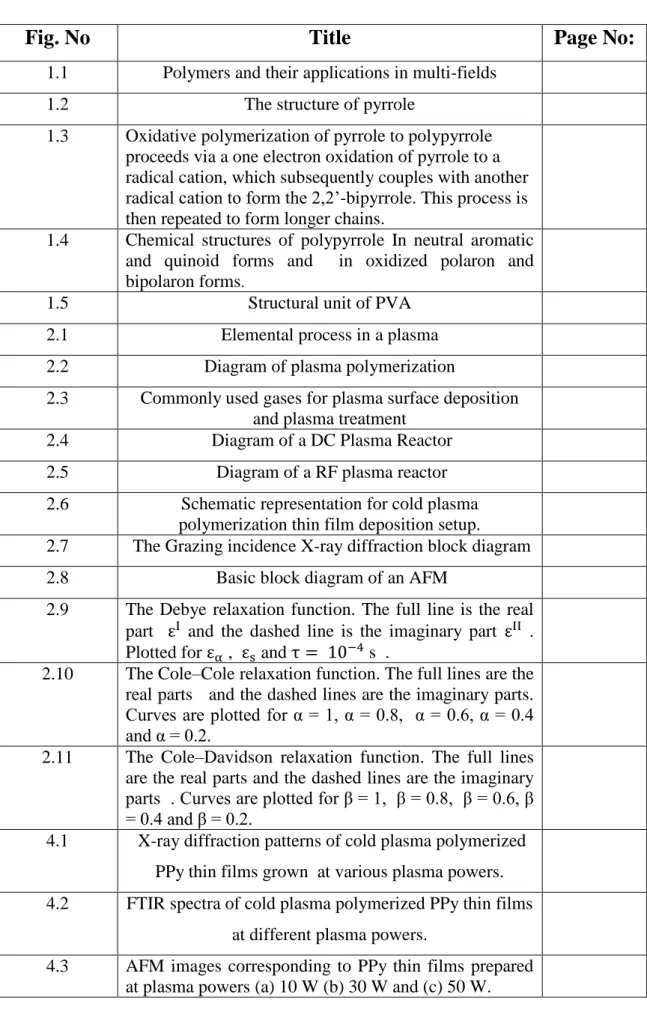
2.9 The Debye relaxation function. The full line is the real part εI and the dashed line is the imaginary part εII . Plotted for εα , εs and τ = 10−4 s .
2.10 The Cole–Cole relaxation function. The full lines are the real parts and the dashed lines are the imaginary parts. Curves are plotted for α = 1, α = 0.8, α = 0.6, α = 0.4 and α = 0.2.
2.11 The Cole–Davidson relaxation function. The full lines are the real parts and the dashed lines are the imaginary parts . Curves are plotted for β = 1, β = 0.8, β = 0.6, β = 0.4 and β = 0.2.
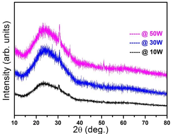
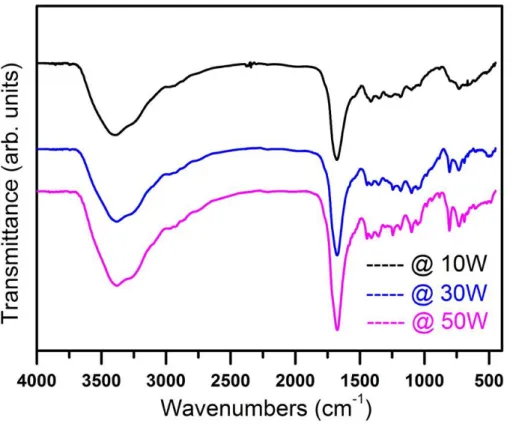
4.1 X-ray diffraction patterns of cold plasma polymerized PPy thin films grown at various plasma powers. 4.2 FTIR spectra of cold plasma polymerized PPy thin films
at different plasma powers.
4.3 AFM images corresponding to PPy thin films prepared at plasma powers (a) 10 W (b) 30 W and (c) 50 W.
4.4 UV – visible absorption spectra for plasma polymerized PPy films at various plasma powers
4.5 Impedance measurements for PPy thin films as a function of plasma powers (a). The variation real impedances as a function of applied frequency in the range 10 mHz – 100 KHz. (b). Nyquist plots (ZII versus ZI) for grown films at various growth conditions.
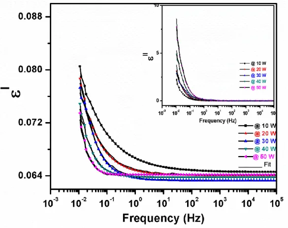
4.6 Behavior of estimated dielectric constants of grown films as a function of frequency (solid black line
represents the fit).
4.7 Cole – Cole plots for plasma polymerized PPy films 4.8 Atomic force micrographs for ‘PVA/AgNPs’ thin films
various temperatures (a) T = 20 oC (b) T = 100 oC (c) T = 200 oC (d) variation of rms roughness.
4.9 Optical absorption spectra for ‘PVA/AgNPs’ thin films at various temperatures in the range 20 oC – 200 oC. 4.10 Plots of the dielectric permittivity vs. log of frequency
(log f) as a function of temperatures for ‘PVA/AgNPs/PVA’ thin films (MLTs).
4.11 Fitting results for dielectric spectrum of ‘PVA/AgNPs/PVA’ thin films (MLTs) at T = 100 o
C: (a) real part, (b) imaginary part.
4.12 Fitting results for dielectric spectrum of ‘PVA/AgNPs/PVA’ thin films (MLTs) at T = 150 o
C: (a) real part, (b) imaginary part.
4.13 The Variation of the loss tangent (tan δ) with frequency at different temperatures for ‘PVA/AgNPs/PVA’ thin films (MLTs).
4.14 The frequency variation of (a) real (MI) and (b) imaginary (MII) parts of electric modulus at different measuring temperatures.
5.1 Interaction of a photon with two energy levels of an atom. Left: Absorption moves the atom from the ground state to the excited state. Middle: Spontaneous emission moves the atom from the excited to the ground state. Right: Induced emission of a photon, by a photon interfering with an atom in the excited state.
5.2 The microcavities according to the confinement method and by according to high Q and ultrahigh Q.
5.3 Photonic crystal structures in various directions.
5.4 Typical transmission spectra T(λ) of a one-dimensional PBG structure.
5.5 The pointing Vectors representation of EM waves in left handed and right handed materials.
5.6 Schematic representation of the possible domains of electromagnetic materials.
5.7 Surface plasmons at interface of Metal and Dielectric films.
5.8 The confined motion of SPPs along metal-dielectric interface.
5.9 (a) A one-dimensional array of grooves of width a,
depth h, and periodicity d. (b) An a × a square holes arranged on a d × d lattice are cut into the surface of a perfect conductor, in which localized surface plasmon modes can be induced by the structure. (c) The dispersion relation [ω(kx)] of the surface bound states
supported by the one-dimensional array of grooves [Fig. 5.9 (a)], with geometrical parameters a/d=0.2 and h/d=1. 5.10 k-space topology: The isofrequency contour for (a) an isotropic dielectric is a sphere, (b) extraordinary waves in a uniaxial medium with extreme anisotropy (εxx = εyy > 0) and εzz < 0 , it is a hyperboloid (type I HMM). (c) Hyperboloid of a type II metamaterial when two components of the dielectric tensor are negative (εxx = εyy < 0) and εzz > 0.
5.11 Schematic of anisotropic multilayer composite. The perpendicular direction is defined as parallel to the normal vector from the surface of the metamaterial and the parallel direction is defined as the plane parallel to the metamaterial interface.
5.12 EMT predicts that a metal dielectric composite can behave as an effective dielectric, effective metal, Type I HMM or Type II HMM depending on the wavelength and fill fraction of the metal. Optical phase diagrams for (a) Ag=Al2O3 multilayer system (b) Ag=TiO2 multilayer
system.
5.13 Schematic of an anisotropic nanowire composite. The perpendicular direction is defined along the long axis of the nanowire and the parallel direction is defined as the plane along the short axis of the nanowire.
5.14 (a) Dispersion of the dielectric constants in a practical multilayer semiconductor realization of the HMM. Note the broadband region in which Type I HMM response is achieved (b) Exact numerical calculation (neglecting loss) in the multilayer structure showing the bloch high-k mode and coupled surface plasmons at the interfaces (c) Evanescent wave incident on an effective medium slab couples to the high-k mode and is transmitted. In contrast, the evanescent wave decays away in vacuum. 6.3.1 E resist cross-section: The electron beam causes
chemical changes in the exposed areas.
6.3.2 E resist crossection: Only the chemically changed e resist can be dissolved in a specific solvent (positive lithography).
6.3.3 E resist cross-section after metal deposition 6.4.1 The general principle in ellipsometry.
6.4.2 Illustration of a thin film on top of a substrate.
6.6.1 Electron configurations for (a) a singlet ground state; (b) a singlet excited state; and (c) a triplet excited state. 6.6.2 Energy level diagram for a molecule showing pathways
for the deactivation of an excited state: vr is vibrational relaxation; ic is internal conversion; ec is external conversion; and isc is an intersystem crossing. The lowest vibrational energy for each electronic state is indicated by the thicker line. The electronic ground state is shown in black and the three electronic excited states are shown in green. The absorption, fluorescence, and
phosphorescence of photons also are shown.
6.6.3 Absorbance spectrum and fluorescence emission spectrum for tyrosine in a pH 7, 0.1 M phosphate buffer. 6.6.4 FluoroLog3-2iHR1-TCSPC-IGA, optical configuration. 6.7.1 Experimental set up used for the lifetime
photoluminescence measurements.
7.2.1 Schematic representation of fabricating steps for HMM structure: (a) Control sample composed of single period of ‘Ag∕Al2O3’ layers (b) Three periods of ‘Ag∕Al2O3’
layers (c) Six periods of ‘Ag∕Al2O3’ layers.
7.2.2 Characterization of HMM: (a) Experimentally determined permittivity values of Ag and Al2O3 thin
films. The red and blue lines represent the real and imaginary permittivity values of Ag, respectively and black line represents the permittivity values of Al2O3.
(b) Real parts of effective permittivity of Ag/Al2O3
HMM determined with effective media theory. The Ag/Al2O3 HMM shows hyperbolic dispersion at λ ≥
430 nm.
7.2.3 (a) Reference sample and (b) dye doped PMMA layer deposited over fabricated HMM structures.
7.2.4 (a) Absorption spectrum of dye dissolved PMMA (for reference sample). (b) Steady-state photoluminescence measurements of dye on reference sample.
7.2.5 Time-resolved photoluminescence measurements of Coumarin dye on Ref and HMM samples. (a) in elliptical region (λe=420 nm), (b) at critical wavelength
(λc=430 nm), and (c) in hyperbolic region (λe=450 nm).
7.2.6 Variation of spontaneous emission lifetimes of the Coumarin dye on Ref and HMM samples, as a function of emission wavelength. (a) first decay time and (b) second decay time.
7.3.1 Two methods of prism-coupling radiation to SPPs; (a) Otto configuration, and (b) Kretschmann-Raether configuration.
7.3.2 Dispersion of a SPP at a metal-dielectric interface (schematic). Lines (a) and (b) illustrate the dispersion of plane waves in the spacer layer (S) and the high index prism (P) respectively where s n is the refractive index of the medium. Only photons (polaritons) with momenta that lie between lines (a) and (b) may couple to SPPs. 7.4.1 Grating geometry and coordinate system used
throughout this thesis. The direction of the electric field vector (E) is illustrated for the situation when p-polarised (TM) radiation is incident.
7.4.2 Fabrication steps for GCHMM: (a) SEM image of designed 2D grating structure over PMMA substrates (b) Dye deposited over HMM (c) Electron beam exposed PMMA layer over dye posited HMM (d) Ag layer (20 nm) deposited over Electron beam exposed PMMA layer over dye posited HMM (e) Ag grating over HMM structure.
7.4.3 Reflectance spectra as a function of excitation wavelength: (a) Reflectance spectrum of various samples obtained at incident grazing angle of 50o. The studied samples are shown in Figs. (b) to (e). The GCHMM sample (iv) shows four prominent reflectance dips corresponding to the excited plasmonic modes (both surface and bulk plasmon polaritons) from the geometry.
7.4.4 Transmittance spectrum of GCHMM at normal incidence. The obtained four prominent transmission maximum correspond to the excitation of plasmonic modes from GCHMM
7.4.5 Reflectance spectra of GCHMM as a function of
incident angle. (a) 430 nm, (b) 450 nm and (c) 480 nm. 7.4.6 Time-resolved photoluminescence measurements of
Coumarin dye on various samples, Ref (pink), HMM (red), HMM with Ag (black), and GCHMM (blue)) with emission wavelength: (a) in elliptical region (λe = 420 nm), (b) at critical wavelength ( λc = 430 nm), and (c) in hyperbolic region (le (λe = 450 nm).
7.4.7 Time-resolved photoluminescence measurements of Coumarin dye on HMM with Ag and GCHMM samples. (a) in elliptical region (λe=420 nm), (b) at
critical wavelength (λc=430 nm), and (c) in hyperbolic
region (λe=450 nm). Red lines represent the
corresponding fit.
7.4.8 Lifetimes of dye on GCHMM and Ag film deposited HMM normalized with respect to HMM sample: for (a) first decay time (t1) and (b) second decay time (t2). The
solid lines are for eye guide. Enlarged plot of normalized decay time of GCHMM is shown in the inset of (a) and (b). Normalized lifetime is studied as a function of emission wavelength from elliptical to hyperbolic dispersion. In the case of GCHMM, a maximum decay rate is observed at 510 nm for both decay times.
8.1.1 Designed two different HMM structures: (a) 5 stacks of Pure PMMA (25 nm) and Ag (12 nm) multilayered HMM structure (b) 5 stacks of “SiO2/DCM dye doped
PMMA/SiO2”(25 nm) and Ag (12 nm) lamellar
DEHMM structure (c) Reference sample.
8.2.2 Real parts of permittivity tensor components HMM evaluated in accordance with effective medium theory. 8.2.3 Steady – state photoluminescence measurements for
reference, dye on top HMM and DEHMM samples. 8.2.4 Emission kinetics of dye molecules on various samples
as a function of emission wavelength at 580 nm. 8.2.5 Variation of (a) first decay time (τ1) and (b) second
decay times (τ2) for reference, dye placed on top of
HMM and DEHMM samples, as a function of emission wavelengths.
8.2.6 Grating coupled DEHMM (GCDEHMM) sample structure
8.2.7 Variation of first decay time (τ1) as a function of
emission wavelengths, for reference, DEHMM and GCDEHMM samples.
List of Tables
Table No. Title Page. No
4.1 Fitting parameters for PPy films deposited at various plasma powers
4.2 Fitting parameters for relaxation process for
‘PVA/AgNPs/PVA’ structured cell at different temperatures. 4.3 Fitting parameters for DC conductivity of
‘PVA/AgNPs/PVA’ structured cell at different temperatures.
5.1 Selection of Metal and dielectric layers for the abrication of HMM structures in various Electromagnetic regions
Part – I. Polymer thin films for
Soft matter applications
1.0
Introduction
The field of ‘Polymer Science and Thin films technology’ is a vibrant contributor to cutting edge advances in the current Science & Technology, not only in its own right, but also due to wide array of industries and technologies made possible by the use of polymer materials. Polymers have unique, molecularly definable properties and process advantages unattainable in any other kind of material. Their attractiveness comes, in part, from the wide varieties of structures, molecular weights and functionalities available via rational synthesis of polymers and their characteristically broad range of possible processing modes. Polymers are the light and flexible materials in nature and human society. Compared with most inorganic structural materials, they are of low density (≈ 1g cm-3).
Polymers form a very significant class of materials without which the life seems very difficult. In everyday human life, they are all around us in different forms such as rubber, in plastic, in resins, and in adhesives and adhesives tapes. The word
polymer is derived from Greek words, poly = many and mers = parts or units of high
molecular mass each molecule of which consist of a very large number of single structural units joined together in a regular manner. In other words, polymers are giant molecules of high molecular weight, called macromolecules, which are build up by linking together of a large number of small molecules, known as monomers. The chemical reaction process, in which the monomers combine to form polymer is known as polymerization [1]
.
Polymers have existed in natural form since life began and those such as DNA, RNA, proteins and polysaccharides play crucial roles in plant and animal life. However, it was not until the middle of the 20th century that we began to understand the true nature of polymers. The utilization of polymeric materials has permeated every facet of our lives and it is hard to visualize today’s world with all its luxury and comfort without man-made polymeric materials. The first generation of man-made polymers was the result of empirical activities and main focus was on chemical composition with virtually no attention paid to the structure. In the first half of 20th century, extensive organic and physical developments had let to the first understanding of the structural concepts of polymers, i.e long chains (or) a network of covalently bonded molecules. In this regard, German chemist H. Standinger studiedsystematically about the polymers and stated that these polymer were composed of giant molecules known as macromolecules [2, 3]. Later, the discovery of nylon by Carothers and his fundamental research work contributed to the elucidation of the nature of polymers. The impetus quest for novel polymer materials to aid in the defense effort during World war II resulted for the discovery of plastics ( such as Polyethylene, polyester resins, acrylonitrile-butadiene-styrene etc.,) which were used to design and fabricate radar cable, telephone handsets, luggage, and safety helmets etc., for military use. The Nobel-prize-winning research work contributions in the field of stereo-specific catalysts led to the ability of polymer chemists to control the properties of polymers, which can be tailor-made for specific applications. Currently, with the existing of advanced technologies it is possible to prepare smart polymers provided with exceptional properties for futuristic applications as represented in the following Figure – 1.1.
1.1 Versatile properties of the polymers
It is worth to mention that, polymers consist exceptional structural features like (i) Intra-molecular features and (ii) Intermolecular features, which make them as versatile.
1..1.1 Intra-molecular features
Generally, polymers consist of characteristic chain-like molecules (i.e monomers), which linked covalently together to form macromolecules. Hence
rotation is possible with respect to covalent bonds and this leads to the rotational isomerism (i.e conformations) and irregularly entangled rather than straight molecules.
1.1.1 (a) Conformations
The conformation of a polymer is the arrangement of the bond orientations both within the backbones, and array side-groups and branches. Basically three specific orientations are there, known as trans, +gauche and –gauche.
1.1.1 (b) Configurations
It explains about the spatial arrangement of the side chemical elements (or) groups of elements about the backbone molecular chains. These configurations establishes during polymerization of the polymers and they cannot be changed by rotations. Configurations provide the information about the arrangements (such as cis
and trans) of identical atoms (or) groups of atoms around a double bond in monomer.
1.1.1 (c) Stereo regularity
The arrangement of side elements/groups around the asymmetric segment of vinyl-type repeating units. Resultantly, three different forms (atactic, isotactic and
syndiotactic) of polymer chain results from head-to-tail addition of the monomers.
Both stereo regularity and configurations provide the information about crystallization and the extent of crystallinity in polymers.
1.1.1 (d) Conjugated chains
The unsaturated alternating single and double bonds are known as conjugated chains. Generally, conjugated polymers demonstrate considerable electrical conductivity.
1.1.1. (e) Branched chains
In this type chains, linear back bone chain coexist with pendant side chains. It occurs during the polymerization of monomers (> 2). The presence of branched chains impedes the ability of polymers to crystallize.
1.1.1.(f) Molecular mass
It represents the number of repeating units in a polymer molecule and it must have a threshold value for the development of polymer properties. Therefore above described characteristic intra-molecular properties influence the glass transition and melting temperatures, crystallinity (or) amorphousness nature, the functionality and frequency of the reactive sites along the backbone chains of polymers.
1.1.2 Intermolecular features
Intermolecular features explains about the bulk properties of polymer.
1.2 Classification of polymers
Polymers can be classified in many different ways based on their source, structure of polymer, mode of polymerization and molecular forces.
1.2.1 Based on source, polymers are classified as follows
(i) Natural polymers:
The polymers which obtain by nature (or) natural resources like plants and animals. These are of considerable importance because they are generally bio-compactable, bio-degradable, non-toxic and non-immunogenic. Due to their exceptional qualities, they can use in Nano drug delivery, pharmaceutical and bio-medical applications, etc., [4 – 7],
(ii) Synthetic polymer:
The polymers which have been synthesized in the laboratory are known as synthetic polymers and are also known as manmade polymers [8, 9].
Eg: Polyvinyl alcohol, polyethylene, polystyrene, polysulfone, etc.
(iii) Semi synthetic polymers:
Chemically modified natural polymers are known as semi synthetic polymer. Hydrogenated natural rubber, cellulose, cellulose nitrate, emthyl cellulose, etc., [10 -12].
1.2.2 Based on structure polymers are classified as linear, branched and cross linked polymers.
Linear polymers:
These polymers consist of long and straight chains. When monomers are joined end-to-end like links along a chain, a polymer with a simple linear structure is formed. In some polymers shorter chains grow off the long chain at certain intervals, so that a branched structure is formed [13]. The examples are high density polythene, polyvinyl chloride, etc. These are represented as follows:
Branched chain polymers:
A polymer chain having branch points that connect three or more chain segments; examples include graft copolymers, star polymers, comb polymers, and dendritic polymers [14].
Cross linked or Network polymers:
A cross-link is a bond that links one polymer chain to another. They can be covalent bonds or ionic bonds. "Polymer chains" can refer to synthetic polymers or natural polymers (such as proteins). When polymer chains are linked together by cross-links, they lose some of their ability to move as individual polymer chains. Cross-links can be formed by chemical reactions that are initiated by heat, pressure, change in pH, or radiation [15].
1.2.3 Based on Polymerization:
Polymers can also be classified on the basis of mode of polymerization into two sub groups.
Additive polymers:
The polymers, which are formed by the repeated addition of monomer molecules possessing double or triple bonds are known as additive polymers, e.g., the formation of polythene from ethane and polypropene from propene. If the addition polymers formed by the polymerization of a single monomeric species are known as homo-polymers, e.g., polythene. The polymers made by addition of polymerization from two different monomers are termed as copolymers, e.g., Buna-S, Buna-N, etc.
Condensation Polymers:
The polymers formed via repeated condensation reactions between two different bi-functional or tri-functional monomeric units, are known as condensation polymers. In these polymerization reactions, the elimination of small molecules such as water, alcohol, hydrogen chloride, etc. take place. The examples are terylene (dacron), nylon 6, 6, nylon 6, etc. For example, nylon 6, 6 is formed by the condensation of hexamthylene diamine with adipic acid.
Based on molecular forces:
The unique mechanical properties of polymers like tensile strength, elasticity, toughness, etc., are significantly governed by intermolecular forces. For example, van der Walls forces and hydrogen bonds present in the polymers [16, 17]. These forces also bind the polymer chains to make the polymers strong and utilize them in various fields. By considering the magnitude of intermolecular forces present in the polymers, they are classified into four groups as follows:
Elastomers:
The polymer, which exhibit “rubber-like” behavior provided with elastic
properties are known as elastomers. In these, polymer chains are bonded by weakest intermolecular forces and make the polymers to stretch by the application of external forces. Due to the presence of few “cross-links” in the polymers, these elastomers can regain their shape after removal of external forces.
Fibers: If the strength of the inter molecular forces are strong (like hydrogen bonds)
and responsible for thread forming solids, are known as fibers. Due to the presence of characteristic hydrogen bonds, they exhibit high tensile strength and high modulus.
Thermoplastic polymers:
The polymers in which strength of intermolecular forces of attrition lies between elastomer and fibers, are known as thermoplastic polymers. These polymers possess linear (or) strong branched type of chain molecules capable of repeatedly softening on heating and hardening on cooling.
Eg: Polythene, polystyrene, polyvinyls, etc.,
Thermosetting plastics:
These polymers are cross linked or heavily branched molecules, which on heating undergo extensive cross linking in moulds and again become infusible. These cannot be reused. Eg: Bakelite, Urea-formaldelyde resins, etc.
1.3 Mechanism of polymerization in polymers
The linking together of a large number of monomers with each together to form a macromolecule (or) polymer molecule through chemical reactions is termed as polymerization. It can also be defined as the fundamental process by which low molecular weight compounds are converted into high molecular weight compounds. Currently, polymerization process is classified into (i) Step growth polymerization and (ii) Chain growth polymerization [18]. The degree of polymerization is related to the molecular mass (M) of the polymer and is given by the equation,
𝐷𝑝 = 𝑀
𝑚 ……….. (1.1)
1.3.1 Condensation Polymerization (or) Step growth Polymerization
Condensation polymerization is a chemical reaction in which polymer is formed and a small molecule of by-product with a lower molecular weight is released. The eliminated by-product is called condensate. The reaction can take place between two similar (or) different monomer, which is also known as step growth polymerization [19, 20].
1.3.2 Addition Polymerization (or) Chain Polymerization
In this polymerization, two (or) more molecules of monomers attach together to form a polymer. In this polymerization, there is no elimination of any molecule. It is a chain reaction and no by product is released. It is obtained by linking together the monomer molecules by a chain reaction to give a polymer whose molecular weight is exactly an integral multiple of that of the monomer as in the case of polyethylene obtained by polymerization of ethylene. Only a single monomer is involved in addition polymerization and hence the polymer is homopolymer and contains the same monomer units, heat (or) a catalyst for opening the double bond of the monomer and creating the reactive sites [above third reference].
1.4
Introduction to Conducting Polymers
The conducting polymers attract attention of researchers and engineers from a variety of fields in science and technology as promising electrode materials for energy storage devices (electro-chemical batteries and capacitors), electro catalysts and biosensors based thereon, photo luminescent and electroluminescent materials, artificial muscles, gas separating membranes, anticorrosive coatings, electromagnetic shields, materials for microlithography, etc. [21]. In addition, the possibilities to produce conducting polymers electrochemically and to control their properties by electrochemical means are of interest on their own. Polymers have long been used as insulating materials. For example, metal cables are coated in plastic to insulate them. However, there are at least four major classes of semiconducting polymers that have been developed so far. They include conjugated conducting polymers, charge transfer polymers, ionically conducting polymers and conductively filled polymers. The conductively filled conducting polymers were first made in 1930 for the prevention of corona discharge. The potential uses for conductively filled polymers have since been multiplied due to their ease of processing, good environmental stability and wide range of electrical properties. The report of electrical conductivity in ionic polymers attracted considerable interest [22]. Since then, various ionically conducting polymers or polymer electrolytes have been prepared for a wide range of applications ranging from rechargeable batteries to smart windows.
The discovery of electrical conductivity in molecular charge transfer (CT) complexes in the 1950s [23] promoted the development of conducting CT polymers,
and led to subsequent findings of superconductivity with molecular CT complexes in 1980 [24] and with fullerene in 1986 [25]. The conductivity in CT complexes arises from the formation of appropriate segregated stacks of electron donor and acceptor molecules and a certain degree of charge transfer between the stacks. In addition, Along with all of the activities described above, various conjugated polymers have been synthesized, which show excellent electrical properties [26]. Owing to the delocalization of electrons in a continuously overlapped π – π* orbital along the polymer backbone, certain conjugated polymers also possess interesting optical and magnetic properties. These unusual optoelectronic properties allow conjugated polymers to be used for a large number of applications, including protecting metals from corrosion, sensing devices, artificial actuators, all-plastic transistors, non-linear optical devices and light emitting displays. Due to the backbone rigidity intrinsically associated with the delocalized conjugated structure, however, most unfunctionalized conjugated polymers are intractable (i.e. insoluble, infusible and brittle). Some of them are even unstable in air.
1.5
Conjugated Polymers
Conjugated polymers are organic macromolecules which consist at least of one backbone chain of alternating double- and single-bonds. Due to the fact that the pz
-orbitals of the carbon atoms which forms the π--orbitals of the alternating double-and single-bonds mesomerize more or less, i.e. the single and double bonds becomes similar, double-bonds overlaps also over the single bonds. Furthermore, the π-electrons can be easier moved from one bond to the other, what makes conjugated polymers to be one-dimensional semiconductors. Conjugated polymers have a framework of alternating single and double C-C, C-S or C-N bonds. The characteristics of the π-bonds are the source of the semiconducting properties of these materials. The difference in energy between the π orbital and an anti-bonding π∗ orbital produces the band gap that determines the electrical and optical properties of the material [27]. Like inorganic semiconductors they can be doped, to increase their conductivity extremely. For the discovery and development of such conductive polymers Alan J. Heeger, Alan G. MacDiarmid, Hideki Shirakawa received the Nobel prize in chemistry 2000. The most simple conjugated polymer is polyacetylene, which consist only of a single chain of alternating single- and double-bonds.
The conductivity of such polymers is the result of several processes. For example, in traditional polymers such as polyethylenes, the valence electrons are bound in sp3hybridized covalent bonds. Such "sigma-bonding electrons" have low mobility and do not contribute to the electrical conductivity of the material. However, in conjugated materials, the situation is completely different. Conducting polymers have backbones of contiguous sp2 hybridized carbon centers. One valence electron on each center resides in a pz - orbital, which is orthogonal to the other three sigma-bonds.
All the pz orbitals combine with each other to a molecule wide delocalized set of
orbitals. The electrons in these delocalized orbitals have high mobility when the material is "doped" by oxidation, which removes some of these delocalized electrons. Thus, the conjugated p-orbitals form a one-dimensional electronic band, and the electrons within this band become mobile when it is partially emptied. The band structures of conductive polymers can easily be calculated with a tight binding model. In principle, these same materials can be doped by reduction, which adds electrons to an otherwise unfilled band. In practice, most organic conductors are doped oxidatively to give p-type materials. The redox doping of organic conductors is analogous to the doping of silicon semiconductors, whereby a small fraction silicon atoms are replaced by electrorich, e.g., phosphorus, or electropoor, e.g., boron, atoms to create n-type and p-n-type semiconductors, respectively. Due to its simple conjugated molecular structure and fascinating electronic properties, polyacetylene has been widely studied as a prototype for other electronically conducting polymers [28].
1.6
Introduction Polypyrrole (PPy)
Organic polymers which are π – conjugated and having hetrocyclic structures have received great attention because of their potential applications. Among the conducting polymers known to date, ones based upon PPy have attracted special interest because of their high conductivity, their ease and high flexibility in preparation, their stability and good mechanical properties. Polypyrrole (ppy) is mostly concentrated due to simple oxidation and easy water solubility of monomer (pyrrole). In addition ppy possesses high conductivity, fast electrochemical switching and high specific capacitance values and environmental stability [29]. Depending on type of preparation routes, PPy can change the electrical and optical properties with size and shape of
nanostructures, which is an important goal in state-of-the-art of material designing [30 – 32]. PPy in thin film form can be used in potential technological applications such as in electronic and electrochromic devices [33 – 35], counter electrode in electrolytic capacitors [36] sensors [37 – 39], chromatographic stationary phases [40], light-weight batteries [41], membrane separation [42] consequently, have attracted a great deal of attentions in recent years and this is currently one of the most active areas of research in polymer science and engineering at present.
Polypyrrole is amorphous and usually gives only a diffuse halo in X-ray diffraction patterns [43, 44]. The electron diffraction showed that there are up 15% (of total volume) of crystalline domains in the bulk of amorphous PPy [45] The experimental data indicate that the crystalline regions have a monoclinic lattice; the pyrrole rings are oriented so that nitrogens of neighboring rings are oriented in opposite directions as show in the following Figure – 1.2.
Figure - 1.2 The structure of pyrrole.
Polypyrrole (PPy) can be formed chemically or electrochemically through oxidative polymerization of pyrrole monomer, Figure – 1.3.
Figure – 1.3: Oxidative polymerization of pyrrole to polypyrrole proceeds via a one electron oxidation of pyrrole to a radical cation, which subsequently couples with another radical cation to form the 2,2’-bipyrrole. This process is then repeated to form longer chains.
The final form of polypyrrole is that of a long conjugated backbone as seen in Figure – 1.4 The polymer has resonance structures that resemble the aromatic or quinoid forms. In this neutral state the polymer is not conducting and only becomes conducting when it is oxidized. The charge associated with the oxidized state is typically delocalized over several pyrrole units and can form a radical cation (polaron) or a dication (bipolaron). The physical form of polypyrrole is usually an intractable powder resulting from chemical polymerization and an insoluble film resulting from electro polymerization.
Figure – 1.4: Chemical structures of polypyrrole In neutral aromatic and quinoid forms and in oxidized polaron and bipolaron forms.
1.7
Poly(vinyl alcohol) (PVA)
In recent years energy conversion devices based on organic semiconductors are an emerging research field with substantial future prospects and it has attracted great attention due to the advantages of light weight, flexibility, and low cost of production with the possibility of fabricating large area devices based on solution processing. Polymeric materials have been the subject of intense scientific and technological research because of their potential applications. In particular, conducting polymers have been extensively investigated in the area of electronics and optoelectronics due to their attractive properties [46, 47]. Polymeric dielectric materials have been preferred because of their dielectric and physical properties over a wide range of temperatures and frequencies. Over the years, among various polymers, poly(vinyl alcohol) (PVA), as one of the most important polymers, has recently received considerable interest, owing to its numerous potential applications in electronic components. It has different internal structure that may be considered as
amorphous or semicrystalline. The semicrystalline structure of PVA showed an important feature rather than of amorphous one. This is because semicrystalline PVA leads to formation of both crystalline and amorphous regions [48 – 50]. PVA polymer is soluble in water and other solvents and is widely used in synthetic fiber, paper, contact lens, textile, coating, and binder industries, due to its excellent chemical and physical properties, nontoxicity, processability, good chemical resistance, high dielectric strength, good charge storage capacity, wide range of crystallinity, good film formation capacity, complete biodegradability, and high crystal modulus dopant-dependent electrical and optical properties [51 – 54]. PVA is comprised of carbon chain backbone with hydroxyl groups attached to methane carbons; these OH groups can be a source of hydrogen bonding and hence assist in the formation of polymer composite. Interestingly, semicrystalline materials have exhibited improvement in certain physical properties due to crystal-amorphous interfacial effect.
PVA is unique among polymers (chemical compounds made up of large, multiple-unit molecules) in that it is not built up in polymerization reactions from single-unit precursor molecules known as monomers. Instead, PVA is made by dissolving another polymer, polyvinyl acetate (PVAc), in an alcohol such as methanol and treating it with an alkaline catalyst such as sodium hydroxide. The resulting hydrolysis, or “alcoholysis,” reaction removes the acetate groups from the PVAc molecules without disrupting their long-chain structure. When the reaction is allowed to proceed to completion, the product is highly soluble in water and insoluble in practically all organic solvents. Incomplete removal of the acetate groups yields resins less soluble in water and more soluble in certain organic liquids. PVA is used in sizing agents that give greater strength to textile yarns and make paper more resistant to oils and greases. It is also employed as a component of adhesives and emulsifiers, as a water-soluble protective film, and as a starting material for the preparation of other resins. The chemical structure of the resulting vinyl alcohol repeating units is shown in the Figure – 1.5.
Experimental
&
2.0
Polymer thin film deposition techniques
In recent years, polymer thin film science has grown worldwide into a major research area. The significance of thin film coatings and the synthesis of new materials for industry have resulted in a tremendous increase of innovative thin film processing technologies. The major exploitation of thin film science is still in development state and goes hand – in – hand with the explosion of scientific and technological break-through in microelectronics, optics and nanotechnology. Currently, rapidly changing needs for thin film materials characterization and fabrication of devices are creating new opportunities for the development of new processes, materials and technologies. Therefore, basic research activities will be necessary to improve knowledge, understanding and to develop predictive capabilities for relating fundamental physical and chemical properties to the microstructure and performance of polymer thin films in various applications. Results of combined experimental and theoretical investigations are prerequisite for the development of new thin film systems and the tailoring of their microstructure and performance.
The thin film technology activity is represented by a relatively new research area, called “SURFACE ENGINEERING”. Surface Engineering has been one of the most expanding scientific areas includes the design and processing of surface layers and coatings, internal interfaces and their characterization. This Surface Engineering is directed by the demands of thin film and surface characteristics of materials. These thin film systems necessitate direct control of materials on the molecular and atomic scale, including surface modifications, deposition and structuring. Many these techniques were accountable for remarkable advances in the fundamental understanding of the physics and chemistry of thin films, their microstructural evolution and their properties. This progress has led to the development of novel materials, expanded applications and new designs of devices and functional thin film systems. It is noteworthy that, the quality of thin films, their microstructural and basic characteristics in a device level mainly depend upon type of thin film deposition techniques. There exists a variety of several physical/chemical vapor thin film deposition techniques/technologies originate from purely physical or purely chemical processes. In this regard various thin film deposition techniques were illustrated and discussed about their respective working principles and limitations in comparison to the other film processing techniques.
2.1 Spin Coating technique
Spin coating is a simple process for rapidly depositing thin coatings onto relatively flat substrates. The substrate to be covered is held by some rotatable fixture (using vacuum to clamp the substrates in place) and the coating solution to spread out and leave behind a very uniform coating of the chosen material on the surface of the substrate. The advantage of spin coating is its ability to quickly and easily produce very uniform films from a few nanometers to a few microns in thickness. The use of spin coating in organic electronics and nanotechnology is widespread and has built upon many of the techniques used in other semiconductor industries but also has some differences due to the relatively thin films, and high uniformity that are required for effective device preparation, as well as the need for self-assembly and organization to occur during the casting process [55, 56].
2.2 Dip coating technique
Dip coating is the precision controlled immersion and withdrawal of any substrate into a reservoir of liquid for the purpose of depositing a layer of material. Many chemical and nanomaterial engineering research projects in academia and industry make use of the dip coating technique. Many factors contribute to determining the final state of the dip coating of a thin film. A large variety of repeatable dip coated film structures and thicknesses can be fabricated by controlling many factors: functionality of the initial substrate surface, submersion time, withdrawal speed, number of dipping cycles, solution composition, concentration and temperature, number of solutions in each dipping sequence, and environment humidity. The dip coating technique can give uniform, high quality films even on bulky, complex shapes. The dip coating technique is used to make thin films by self-assembly and with the sol-gel technique. Self-assembly can give film thicknesses of exactly one monolayer. The sol-gel technique creates films of increased, precisely controlled thickness that are mainly determined by the deposition speed and solution viscosity [57 – 59].
2.3 Solution casting technique
Polymer films can be prepared by two distinct casting techniques, which are (i) Free casting technique and (ii) Blade casting technique.
(i) Free casting technique:
In free casting (FC) technique, pre-prepared polymer solution at optimized conditions, is poured onto a flat-bottomed glass cup without imposing hydrodynamic stress on the liquid. The solvent is allowed to evaporate under ambient conditions until the film hardens. The hardened film is then removed from the cup by washing it off with distilled water and placed in a vacuum oven at 100 0C for 12 h for final drying. DSC and gas chromatography data indicated that this procedure was effective in removing residual solvent and moisture from the film. The thickness of films produced by this method is dependent in a straightforward way on concentration and the volume of liquid in the cup. In this study, the concentration was varied in the range 1-8 (wt/wt) % and the liquid volumes ranged from 5 to 20 mL yielding film thicknesses of 12- 200 pm. The lower limit is due to difficulties in producing self-supporting films with uniform thickness while attempts to produce films thicker than 200 pm usually led to various gross defects, such as ”orange peel”, on the film surface [60].
(ii) Blade casting technique:
In blade casting (BC) technique, pre-prepared polymer solution is poured onto surface of a substrate and a knife blade uses to spread the liquid over a flat glass substrate. In this process, considerable hydrodynamic stresses are generated during the coating step. Since the liquid films produced are relatively thin, initial solvent removal from the cast layer was relatively fast under ambient conditions-the films were hard to the touch within minutes. The coatings are left at ambient for ca. 12 h, and final solvent is removed by placing the coated substrates in a vacuum oven at 25oC for few hours. After removal from the oven the coatings are soaked in distilled water, peeled off the substrate, and dried again in vacuum for 2 h at 60 oC. It is important to note that the order of peeling the film from the substrate, i.e., before or after drying in the oven, has a significant effect on the properties of the film. The final film thickness was dictated by the blade height and the concentration. The effect of blade height on the thickness of the deposited film can be estimated from the coating dynamics of a slot coater, and the effect of concentration derives from a simple mass balance. The blade height is varied in the range 120 - 760 μm and the concentrations used were 5-20 (wt/wt) %, producingthicknesses in the range 12 - 114 μm [61].
In this technique, the limitations are dictated by difficulties in controlling thickness uniformity (for the thin films) and various surface defects (for the thick films). In both methods, but especially in the BC process, air currents above the drying layers and exceedingly fast drying produced “orange peel” defects on the dried films. To circumvent this problem, the BC films were enclosed in a glass box and a lid was placed on the FC cups while the films were drying at ambient. This slowed down the evaporation rate yielding films with good clarity. Some of the films became opaque due to spontaneous crystallization during the initial drying step. This is prevalent in the thick polycarbonate films. When the enclosing box was gradually removed, the drying rate was increased and the crystallization process could be effectively suppressed.
2.4 Electrochemical polymerization
In polymers thin films technology, the emergence of advancements made in electrochemical polymerization (ECP) technique which is a fast developing field interfacing polymer science and electrochemistry. It provides a novel approach to the synthesis of conducting polymers. ECP is normally carried out in a single compartment electrochemical cell by adopting a standard three electrodes configuration and typically electrochemical bath consists of a monomer and a supporting electrolyte dissolved in appropriate solvent. ECP can be carried out either potentiostatically (i.e. constant voltage condition) or galvanostatically (i.e. constant current condition) by using a suitable power supply. Potentiostatic conditions are recommended to obtain thin films while galvanostatic conditions are recommended to obtain thick films [62, 63].
2.5 Spray – coating technique
Spray coating in general includes the formation of fine droplets of a coating solution and their deposition and coalescence on a substrate. The liquid to be used for coating breaks up into small droplets by atomization in the spray nozzle. The generated droplets are then deposited on a substrate kept below the spray nozzle where they coalesce to form a coating. Conventionally, air pressure is used for the atomization where the liquid coming through the nozzle is broken down into tiny droplets upon passage through a narrow orifice [64]. Alternatively, the ultrasonic atomization technique, in which high frequency sound vibration generates a fine mist of solution, is used for spray coating and often preferred over pneumatic atomization [65].
Overall, the advantages of ultrasonic spray coating are as follows: simplicity, good transfer efficiency, economical, precise conformal coating on planar and nonplanar surfaces, generation of small droplets in the micrometer range, and good reproducibility [66, 67]. Spray coating is associated with many material and process parameters which must be controlled in order to obtain a uniform film. The concentration of the polymer solution, the solvent used, the substrate on which the solution is sprayed, the number of spray passes, the flow rate of the polymer solution, the temperature of the substrate, the distance between the spray nozzle and the substrate, the speed of the moving nozzle during spraying, and the air pressure which transports the sprayed droplets to the substrate are all to be taken into consideration.
2.6 Thermal Evaporation technique
Thermal evaporation technique is one of the widely used deposition technique for the preparation of polymer thin films. The physical stages of film formation consists of several distinguishable steps of film as (1) sublimation of the material to be deposited to the vapor phase, (2) transfer of vapors from the evaporant to the substrate, (3) condensation of vapors upon arrival on the substrate and their rearrangement or modifications of their building on the substrate surface. In this method, materials sublime at lower temperature under vacuum and mean free path of the vapor atoms is considerably large at lower pressure and hence a sharp pattern of the film is obtained. The characteristics of the films are influenced by rate of evaporation, pressure during deposition, thickness of the film, angle of evaporation, temperature of the substrate and residual atmosphere. All these parameters can be controlled in the thermal evaporation technique [68, 69].
Resistive heating is one of the simple and versatile physical vapor deposition techniques, using which a large variety of materials can be evaporated onto different substrates. In this method, the material to be deposited is heated resistively or radiative to a very high temperature in a very low pressure (< 10-6 Torr) till it vaporizes. The vapor species thus created in extremely clean ambient are transported through vacuum to condense on the substrates placed above the source to form a pure
film. A variety of heating sources are used to evaporate materials depending on the form of availability such as wire, powder, foil, solid etc., of the evaporate material.
2.7 Sputtering technique (a) DC sputtering:
When the surface of a material is bombarded with high velocity positive ions, the atoms of the surface will be ejected, this phenomenon is known as sputtering. The atoms ejected from the surface can be condensed on a substrate to form a thin film. The energetic particles, which cause sputtering, may be ions, neutral atoms, neutrons, electrons or protons. Most sputtering applications are performed by the bombardment with ions. The sputtering yield is the most important parameter for characterizing the sputtering process. The sputtering yield depends on the bombarded material, its structure, composition, the characteristics of the incident ion and also the experimental geometry. Now a day the sputtering has become one of the most versatile techniques in thin film technology for preparing the thin films of almost all the material [70].
(b) RF sputtering:
It is difficult to sputter the insulating target by DC sputtering. If an insulator target is substituted for metal target, a surface positive charge built upon the front surface of the insulator during ion bombardment. This charge build up can be prevented by simultaneous bombardment of the insulator with ion beam and electron beam particles. Alternatively, applying a RF potential to the metal electrode placed behind the dielectric plate target can prevent the charge accumulation on the surface. At RF potential, the electrons oscillating in the alternating field have sufficient energies to cause ionizing collisions and the discharge will be sustained. The high voltage at the cathode, which is essential in a DC glow discharge for the generation of secondary electrons, is no longer required here for the discharge to maintain itself. Since the electrons have much higher mobility than ions, many more electrons will reach the dielectric target surface during the positive half-cycle than ions during the negative half – cycle, and the target will become self – biased negatively. The negative DC potential on the insulating target surface repels electrons from the vicinity of this surface, creating an enriched sheath.
The ions in front of the target bombard the target and process the sputtering. It should be noted that since the applied RF field appears between the two electrodes, an electron escaping from the inter electrode space as result of random collision will no longer oscillate in the RF field. Therefore, these electrons will not get sufficient energy to cause ionization hence will be lost from the glow. But if magnetic field is applied parallel to the RF field, it will constrain the electrons without being lost to the flow, thus improving the efficiency of the RF discharge. So a magnetic field is more important in RF sputtering than in the DC case. A grounded metal is placed close to the other side of the metal electrode to extinguish the glow on the electrode side and to prevent sputtering of the metal electrode. Thin films of quartz, aluminum oxide, boron nitride and various glasses have been prepared using RF sputtering. Although good quality films have been prepared by sputtering, this technique has the disadvantage of being a low deposition rate process. Moreover, the films produced by sputtering require a post-deposition heat treatment in appropriate ambient conditions [71, 72].
2.8 Chemical Vapor Deposition technique
The CVD technique has been the most commonly employed thin-film deposition technique in the industry for the deposition of inorganic thin films, due to the robustness and the low cost of the process [73]. CVD of inorganic films requires high substrate temperatures and high powers which would damage the functional groups of the polymer and lead to undesirable crosslinking, therefore, CVD is traditionally not compatible with polymer thin-film deposition. However, through modifications of the CVD reactants or reactor designs, polymer depositions at low temperatures and low-energy inputs can be achieved, making CVD a widely used technique for polymer deposition [74]. Deposition of highly cross-linked, insoluble polymers, copolymers of incompatible monomers (organic networks) or conducting polymers can easily be achieved using CVD. The CVD also allows the application-specific tuning of the chemical compositions of the copolymers to achieve the desired response. The polymer CVD techniques can be categorized according to the polymerization mechanism, such as chain-growth and growth of polymers.