0.13
µm CMOS Technologies
for Analog Front-end Circuits in LHC Detector Upgrades
M. Manghisoni, V. Re, G. Traversi
Università di Bergamo, Dipartimento di Ingegneria Industriale, Viale Marconi, 5, 24044 Dalmine, Italy and, INFN, Sezione di Pavia, Via Bassi, 6, 27100 Pavia, Italy
[email protected], [email protected], [email protected]
L. Ratti, V. Speziali
Università di Pavia, Dipartimento di Elettronica, Via Ferrata, 1, 27100 Pavia, Italy and, INFN, Sezione di Pavia, Via Bassi, 6, 27100 Pavia, Italy
[email protected], [email protected]
Abstract
Deep submicron CMOS technologies are widely used for the implementation of low noise front-end electronics in various detector applications. In this field the designers’ effort is presently focused on 0.13 µm technologies. This work presents the results of noise measurements carried out on CMOS devices in a 0.13 µm commercial process. The study also includes an evaluation of the impact of high doses of ionizing radiation on the noise performances. Data obtained from the measurements provide a powerful tool to model noise parameters and establish design criteria in a 0.13 µm CMOS process for detector front-ends in LHC upgrades.
I. I
NTRODUCTIONSubmicron CMOS technologies provide well-established solutions to the implementation of low noise front-end electronics for a wide range of detector applications. The advantages in the design of high performance mixed signal systems were exploited in recent years and led to the fabrication of integrated circuits in 0.35 µm and 0.25 µm CMOS processes [1-4]. Following the trend of commercial silicon foundries, the IC designers’ effort is gradually shifting to 0.13 µm CMOS generations, to implement readout integrated circuits for silicon strip and pixel detectors, in view of future applications (LHC upgrades, Linear Collider, Super B-Factory) [5-8]. Furthermore, a beneficial side effect of CMOS scaling is that the technology becomes harder for every new generation [9]. This observation is related to the thickness reduction of both the gate and isolation dielectric layers, making them less susceptible to ionization damage. However, it is very important to assess the impact of technology scaling on the noise parameters, which can be affected by gate oxide quality and short-channel phenomena. This can be very critical in applications such as LHC upgrades, where a very short signal shaping time is required because of high event rate, or where a thin silicon detector (100 µm or less) is mandatory for material minimization or radiation hardness. In this paper we have the opportunity to discuss a very large set of experimental results relevant to a commercial CMOS process with minimum gate length of
0.13 µm and manufactured by STMicroelectronics. The analysis of the experimental results includes the comparison of white and 1/f noise components of PMOS and NMOS devices characterized at drain currents from several tens of
µA to 1 mA, that is, the usual operating currents of input
MOSFETs in integrated charge-sensitive preamplifiers. In these conditions, deep submicron devices are biased in weak or moderate inversion. In this study an evaluation of the impact of ionizing radiation on the analog performances is also reported and discussed. An interesting point is to verify if standard open structure devices can be safely used in rad-hard circuits, without implementing any special radiation hard technique. Special attention is given to the behavior of white and 1/f components in the noise voltage spectrum. Experimental results point out that open structure devices in the examined 0.13 µm technologies exhibit a large degree of tolerance to ionizing radiation. This may be exploited to remove geometry constraints and increase functional density.
II. E
XPERIMENTALD
ETAILSA. Investigated Devices
The MOSFETs studied in this paper belong to a commercial CMOS process with minimum gate length of 0.13 µm and manufactured by STMicroelectronics. The oxide thickness tOX is 2.4 nm, COX, the gate capacitance per unit area, is about 14.8 fF/µm2 and the maximum allowed supply voltage VDD is +1.2 V. We studied devices with different gate length L ranging from 0.13 µm to 1 µm and with a gate width ranging from 100 µm to 1000 µm. Devices with such a large W are commonly used as front-end elements in readout systems for particle detectors, in order to achieve the best noise performances [11]. NMOS were laid out using a standard open structure configuration, without implementing any special radiation hardening techniques.
B. Measurement Setup
The device parameters were characterized at drain currents ID below 1 mA, as dictated by power dissipation constraints in
high density monolithic front-end systems. The gate-referred noise voltage spectrum was measured using instrumentation purposely developed at the Electronic Instrumentation Laboratory, University of Pavia. The noise of the DUT is amplified by a wideband interface circuit and detected by a Network/Spectrum Analyzer HP4195A [12]. Measurements of static and signal parameters were carried out with a Semiconductor Parameter Analyzer HP4145B. The value of the transconductance gm as a function of the drain current ID was extracted from ID-VGS curves.
III. E
XPERIMENTALR
ESULTSA. Noise equations
The noise performances of a MOS device can be characterized in terms of the gate referred noise voltage spectrum Se(f) which can be modeled by means of the
equation: f α i f 2 W 2 e
f
1
C
K
S
(f)
S
=
+
. (1)The first term in (1) is determined by channel thermal noise and noise contributions from parasitic source/drain, gate and bulk resistors. In the low density operating region the contributions from these resistors usually have a minor impact. Therefore, Sw2 is dominated by channel thermal noise and can be expressed by the relationship:
m 2 W
g
Γ
4kT
S
=
(2) m [nVwhere Γ is the coefficient of the channel thermal noise, depending on the inversion region, k is the Boltzmann’s constant, T is the absolute temperature and gm is the device transconductance. The value of the coefficient Γ depends on the degree of channel inversion and on the effect of the bulk on the transconductance gm; in submicron devices it may be increased by short channel effects such as mobility reduction and hot carriers. The second term in (1) is given by 1/f noise in the channel current. Kf is an intrinsic process parameter for
0.1 1 10 100 103 104 105 106 107 108 W/L=1000/0.2 ID=1 mA, |VDS|=0.6 V N o is e V o ltage S pec tr um [nV /Hz 1/2 ] Frequency [Hz] 1/f Slope NMOS PMOS
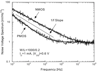
Figure 1: Gate referred noise voltage spectra for NMOS and PMOS devices with W/L=1000/0.2 (ID=1 mA, |VDS|=0.6 V).
1/f noise and Ci is the gate capacitance, whose value depends on the size of the MOSFET, Ci=COXWL. W is the gate width, L is the gate length. The exponent αf determines the slope of this low frequency noise term and its value is usually close to
αf=1. The analysis of the experimental results includes the comparison of white and 1/f noise components of PMOS and NMOS devices characterized at different drain currents.
B. Analysis of noise measurement results
Fig. 1 compares the noise voltage spectra of a PMOS and an NMOS with the same gate dimensions. The devices are biased at ID=1 mA, that is in the moderate inversion region, where the NMOS has a larger transconductance with respect to the PMOS. This results in a smaller channel thermal noise for the NMOS, as it appears in the high frequency part of the spectra. The PMOS retains an advantage on the NMOS in terms of 1/f noise, which dominates the low frequency portion of the spectra. It can be observed that the slope of the low frequency component of the spectrum differs from the case
αf=1. For all the examined devices, values of αf≥1 were found for the PMOS, while αf≤1 for the NMOS. This behavior was detected in other deep submicron processes [13-15] and could be related to a different profile of oxide traps interacting with carriers of different polarity.
0.1 1 10 100 103 104 105 106 107 108 L=0.13 µm L=0.35 µm L=1.00 µm Noi se V olt age S pec tr u /Hz 1/2 ] Frequency [Hz] NMOS W=1000 µm ID=250 µA
Figure 2: Noise voltage spectra of NMOS with gate width W=1000 µm and different gate length L (ID= 250 µA, VDS=0.6 V).
The behavior of the 1/f and white noise terms is studied as a function of the device polarity and of the gate length and width to account for different detector requirements. Fig. 2 shows noise voltage spectra for NMOS devices with gate lengths L ranging from 0.13 µm to 1 µm. Since the devices are biased close to weak inversion, white noise should not be sizably affected by L variations. Actually, this is true except for the device with the minimum channel length allowed by the technology (L=0.13 µm) which exhibits a larger thermal noise. This may be explained by short channel effects increasing the value of the coefficient Γ. At low frequencies, 1/f noise increases with decreasing L. According to (1), this is due to the reduction in the input capacitance Ci. However, at short channel lengths 1/f noise is higher than predicted by Ci scaling. In fact, the value of the coefficient Kf extracted from
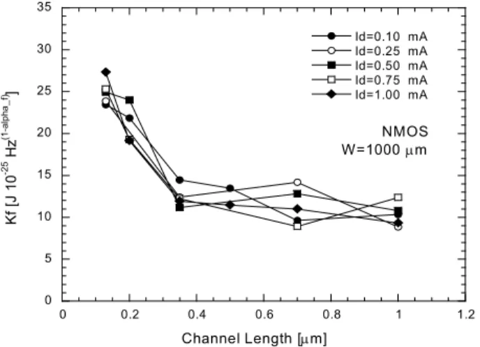
measurements on NMOS with L<0.5 µm is larger than for devices with longer channels, as shown by Fig. 3. As it was also found in other deep submicron technologies [11,13], both white and 1/f noise data suggest that using the minimum channel length for NMOS devices implementing low-noise functions should be avoided.
0 5 10 15 20 25 30 35 0 0.2 0.4 0.6 0.8 1 1.2 NMOS W=1000 µm Id=0.10 mA Id=0.25 mA Id=0.50 mA Id=0.75 mA Id=1.00 mA K f [J 1 0 -2 5 Hz (1 -a lp ha _ f) ] Channel Length [µm]
Figure 3: 1/f noise coefficient Kf as a function of the gate length L for NMOS with W=1000 µm (|VDS|=0.6 V).
The slope of the 1/f noise term α as a function of the gate length for different values of the bias current ID is shown by Fig. 4. It appears that in the examined region, the parameter αf does not exhibit any clear dependence on the channel length L nor on the drain current ID.
0 0.5 1 1.5 2 0 0.2 0.4 0.6 0.8 1 1.2 Id=0.10 mA Id=0.25 mA Id=0.50 mA Id=0.75 mA Id=1.00 mA al ph a f Channel Length [µm] PMOS NMOS
Figure 4: Slope of the 1/f noise term as a function of the gate length L for NMOS and PMOS devices with W=1000 µm (|VDS|=0.6 V).
Typical values of the slope coefficient of the low frequency noise component obtained for devices of both the polarity are reported in Table 1.
Table 1: Slope coefficient of the low frequency noise term.
αf NMOS 0.85 ± 0.04 PMOS 1.19 ± 0.04
Fig. 5 shows the typical dependence of the noise voltage
spectrum of an NMOS on the drain current ID. Channel
thermal noise is reduced by increasing ID in agreement with
(2), since the transconductance correspondingly increases,
while the 1/f noise component is not affected by ID variations.
0.1 1 10 100 103 104 105 106 107 108 ID=0.10 mA ID=0.25 mA ID=1.00 mA N oi se V olta ge S pe ctr um [nV /H z 1/ 2 ] Frequency [Hz] NMOS W/L=1000/0.35
Figure 5: Noise voltage spectra of an NMOS with W/L=1000/0.35 at different values of ID (VDS=0.6 V).
Measurements on PMOS devices show the same results
for white noise and coefficient αf, while a sizable increase of
Kf both with the channel length L and the drain current ID is
detected. According to [16] this behavior is due to the origin of flicker noise that, in p-channel devices, is often attributed
to mobility fluctuations, and shows an increase of Kf with the
overdrive voltage (VGS-VT) and, therefore, with the drain
current as reported in Fig. 6. For devices with different gate geometries and operating at the same drain current an higher channel length requires an higher overdrive voltage. This
corresponds to an increase of Kf as shown in Fig 7.
0 20 40 60 80 100 120 0 0.2 0.4 0.6 0.8 1 1.2 L=0.20 µm L=0.50 µm L=1.00 µm Kf [J 10 -25 Hz (1-al p ha _f) ]
Drain Current [mA]
PMOS W=1000 µm
Figure 6: 1/f noise coefficient Kf as a function of the drain current ID for PMOS with W=1000 µm (|VDS|=0.6 V).
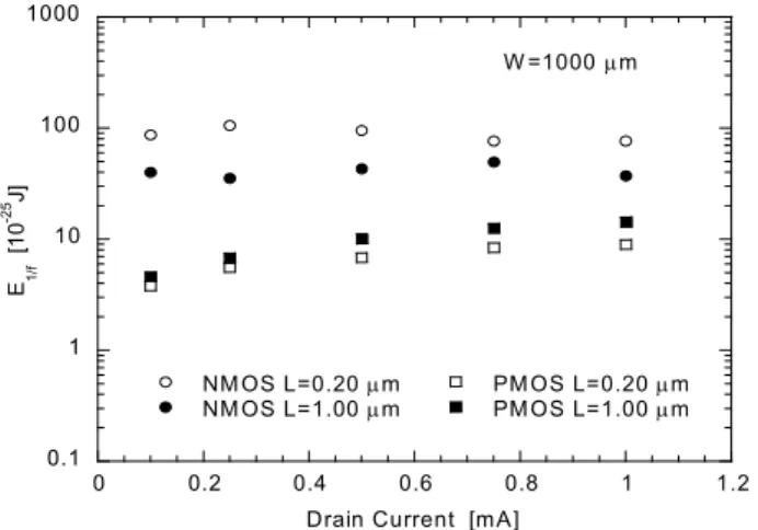
Figs. 3, 6 and 7 also show that NMOS devices feature a
smaller value of Kf with respect to PMOS, even if in the low
frequency region they have definitely larger noise voltage spectra. Actually this parameter is a measure of 1/f noise “energy” in joule [17] if the 1/f noise slope is equal to 1.
0 20 40 60 80 100 120 0 0.2 0.4 0.6 0.8 1 1.2 Id=0.10 mA Id=0.25 mA Id=0.50 mA Id=1.00 mA Kf [J 10 -25 Hz (1 -a lpha _f) ] Channel Length [µm] PMOS W =1000 µm
Figure 7: 1/f noise coefficient Kf as a function of the gate length L for PMOS with W=1000 µm (|VDS|=0.6 V).
If αf≠1, as in the examined 0.13 µm processes, a better understanding of 1/f noise properties can be achieved by using the parameter E1/f(f): f 1 f f / 1 ( f ) K f E = −α (3)
Fig. 8 shows the behavior of E1/f(f) at different drain currents for NMOS and PMOS devices. Here E1/f(f) is evaluated at f=10 kHz, that is, at a frequency where the 1/f noise contribution is sizable for both PMOS and NMOS. The 1/f noise contribution appears to be larger in NMOS by about a factor of 10 for devices with the minimum channel length while a lower difference appears for longer channels.
0.1 1 10 100 1000 0 0.2 0.4 0.6 0.8 1 1.2 NM OS L=0.20 µm NM OS L=1.00 µm PM OS L=0.20 µmPM OS L=1.00 µm E 1/ f [ 1 0 -25 J]
Drain Current [mA]
W =1000 µm
Figure 8: E1/f(f) at different drain currents for NMOS and PMOS devices, evaluated at f=10 kHz.
C. Radiation Effects on Noise
The investigated devices were irradiated up to a 10 MRad(SiO2) total dose with γ-rays from a 60Co source at a dose rate of about 17 Rad(SiO2)/s. The MOSFETs were biased during irradiation in the worst-case condition, that is, with all terminals grounded, in the case of the PMOS devices, and with +1.2 V (maximum voltage allowed by the technology) on the gate relative to source, drain and body in the case of the NMOS devices.
0.1 1 10 100 103 104 105 106 107 108 N oi se V olta ge S pect rum [ nV/ H z 1/ 2 ] Frequency [Hz] W /L=1000/0.35 I D=1 mA before irradiation 10 MRad NMOS PM OS
Figure 9: Noise voltage spectra before and after exposure to γ-rays (10 MRad integrated dose) of a PMOS and an NMOS with
W/L=1000/0.35 at ID=1 mA. 0.1 1 10 100 103 104 105 106 107 108 N oi se V o ltag e S pe ct rum [n V/ H z 1/2 ] Frequency [Hz] W /L=1000/0.35 I D=0.1 m A before irradiation 10 MRad NMOS PM OS
Figure 10: Noise voltage spectra before and after exposure to γ-rays (10 MRad integrated dose) of a PMOS and an NMOS with
W/L=1000/0.35 at ID=0.1 mA.
The behavior of the 1/f and channel thermal noise components was monitored before and after irradiation. Figs. 9 and 10 show data relevant to a PMOS and an NMOS with W/L=1000/0.35 biased respectively at ID=1 mA and ID=0.1 mA. Channel thermal noise is affected to a very limited extent by ionizing radiation, in agreement with the very small post-irradiation decrease of the transconductance gm. For the PMOS device, the increase of 1/f noise is also very small. This reduced 1/f noise sensitivity, likely to be associated with the thinner gate oxide and correlated to the reduced threshold voltage shift, was also found in NMOS with a relatively long channel (L>0.5 µm). In short-channel NMOS devices, instead, at low ID (around 100 µA) 1/f noise increase is much larger than at higher drain currents. This behavior, which was not seen in previous CMOS generations, could be correlated with the ID increase observed in the subthreshold region of the ID-VGS curves. In irradiated short-channel NMOS, this increase might be explained by a sidewall leakage current contribution associated to the STI regions [18,19]. This would mean that at ID values around 100 µA the shallow trench oxide contributes to the 1/f noise
properties of the device. In fact, since it is considerably thicker than the gate oxide, a large 1/f noise increase is expected if, after irradiation, it affects ID to a sizable extent. This behavior my be an important limitation to the use of short-channel, open structure devices in low-noise, low-power analog circuits.
IV. C
ONCLUSIONSThe paper presented a noise characterization of devices in a 0.13 µm CMOS technology. The analysis of the experimental results show that the behavior of the white noise term is consistent with equations valid for long-channel devices. As expected from past experience on previous CMOS generations, 1/f noise is dependent on the fabrication technology and it is very difficult to derive a general law correctly describing the impact of this noise term. Low-noise design requires to keep it under control by an accurate experimental characterization. Experimental results show that the 0.13 µm CMOS technology exhibits a large degree of tolerance to ionizing radiation, taking advantage of the very thin gate oxide, and it is suitable to the design of rad-hard analog circuits. However, limitations concerning short-channel NMOS may arise when they are operated at low drain current, probably because of effects associated with the shallow trench isolation region. Therefore this suggests that low-noise NMOS should be implemented with an enclosed, edgeless structure. Work is currently in progress to extend the experimental analysis to 0.13 µm devices from different foundries, with the goal of defining a more complete overview of the noise performances achievable with this CMOS generation.
V. R
EFERENCES[1] W. Snoeys, F. Faccio, M. Burns, M. Campbell, and E. Cantatore, et al., “Layout techniques to enhance the radiation tolerance of standard CMOS technologies demonstrated on a pixel detector readout chip”, Nucl.
Instrum. Methods Phys. Res. A, vol. A439, p. 349, 2000.
[2] P.F. Manfredi, and M. Manghisoni, “Front-end electronics for pixel sensors”, Nucl. Instrum. Methods
Phys. Res. A, vol. A465, p. 140, 2001.
[3] G. Anelli, F. Faccio, S. Florian, and P. Jarron, “Noise characterization of a 0.25 µm CMOS technology for the LHC experiments”, Nucl. Instrum. Methods Phys. Res. A, vol. A457, pp. 361-368, 2001.
[4] D.C. Christian, J.A. Appel, G. Cancelo, J. Hoff, S. Kwan, A. Mekkaoui, and R. Yarema, et al., “FPIX2: a radiation-hard pixel readout chip for BTeV”, Nucl. Instrum.
Methods Phys. Res. A, vol. A473, pp. 152-156, 2001.
[5] G. Cervelli, A. Marchioro, and P. Moreira, “A 0.13-µm CMOS serializer for data and trigger optical links in particle physics experiments”, IEEE Trans. Nucl. Sci., vol. 51, no. 3, pp. 836-841, 2004.
[6] F. Faccio, et al, “Radiation tolerance of a 0.13 µm commercial CMOS technology”, 5th International
Meeting on Front-End Electronics, June 30–July 3, 2003,
Snowmass, Colorado. http://www-ppd.fnal.gov/EED
Office-w/Conference/FEE_2003/FEE2003.html
[7] V. Re, M. Manghisoni, L. Ratti, V. Speziali, and G. Traversi, “Design criteria for low noise front-end electronics in the 0.13 µm CMOS generation”, paper presented at the 10th European Symposium on Semiconductor Detectors, Wildbad Kreuth (Germany), June 12-16, 2005. To be published in Nucl. Instrum.
Methods Phys. Res. A.
[8] L. Ratti, M. Manghisoni, V. Re, V. Speziali, and G. Traversi, et al., “Novel monolithic pixel detectors in a 0.13 µm CMOS technology with sensor level analog processing”, paper presented at the 10th European Symposium on Semiconductor Detectors, Wildbad Kreuth (Germany), June 12-16, 2005. To be published in
Nucl. Instrum. Methods Phys. Res. A.
[9] E. Simoen, et al, “Short-channel radiation effect in 60 MeV proton irradiated 0.13 µm CMOS transistors”,
IEEE Trans. Nucl. Sci., vol. 50, no. 6, pp. 2426-2432,
Dec. 2003.
[10] V. Re, M. Manghisoni, L. Ratti, V. Speziali, and G. Traversi, “Total Ionizing Dose Effects on the Analog Performance of a 0.13 µm CMOS Technology”, paper presented at the 2005 IEEE Nuclear and Space Radiation Effects Conference (NSREC) in Seattle, Washington (USA), July 11-15, 2005.
[11] M. Manghisoni, L. Ratti, V. Re, and V. Speziali, “Submicron CMOS technologies for low-noise analog front-end circuits”, IEEE Trans. Nucl. Sci., vol. 49, no. 4, pp. 1783-1790, Aug. 2002.
[12] M. Manghisoni, L. Ratti, V. Re, and V. Speziali, “Instrumentation for noise measurements on CMOS transistors for fast detector preamplifiers”, IEEE Trans.
Nucl. Sci., vol. 49, no. 3, pp. 1281-1286, Jun. 2002.
[13] G. De Geronimo, and P. O'Connor, “MOSFET optimization in deep submicron technology for charge amplifiers”, 2004 IEEE Nuclear Science Symposium Conference Record, Vol. 1, 16-22 Oct. 2004, pp. 25-33. [14] R. Jayaraman, and C. G. Sodini, “A 1/f noise technique to
extract the oxide trap density near the conduction band edge of silicon”, IEEE Trans. Electron Devices, vol. 36, no. 9, pp. 1773-1782, Sept. 1989.
[15] K. W. Chew, K. S. Yeo, and S.-F. Chu, “Effect of technology scaling on the 1/f noise of deep submicron PMOS transistors”, Solid-State Electronics, vol. 48, no. 7, pp. 1101-1109, 2004.
[16] Y.P. Tsividis, Operation and Modeling of the MOS
Transistor. Second Edition, Mc Graw-Hill 1999.
[17] V. Radeka, Low-Noise Techniques in Detectors, Ann. Rev. Nucl. Part. Sci. 38 (1988) 217.
[18] M. Turowski, A. Raman, and R. D. Schrimpf, “Nonuniform total-dose-induced charge distribution in shallow-trench isolation oxides”, IEEE Trans. Nucl. Sci., vol. 51, no. 6, pp. 3166-3171, Dec. 2004.
[19] G. U. Youk, et al, “Radiation-enhanced short channel effects due to multi-dimensional influence from charge at trench isolation oxides”, IEEE Trans. Nucl. Sci., vol. 46, no. 6, pp. 1830-1835, Dec. 1999.