1
Le informazioni contenute nel presente documento,
titolo: Innovative techniques for conformal doping of semiconductors for applications in micro- and nano-electronics
autore: Sebastiano Caccamo
consegnato mezzo e-mail in data: 15/09/2017
sono strettamente riservate e confidenziali e sono indirizzate
esclusivamente al destinatario. In accordo fra il Fornitore (Sebastiano Caccamo) ed il Destinatario (Prof. Neri Fortunato, Dott. Arena Giuseppe e Prof.ssa Maria Grazia Grimaldi ) tali informazioni riservate sono divulgate esclusivamente con lo scopo di valutare i requisiti di ammissibilità.
Il Destinatario si impegna a non divulgare a terze parti le Informazioni riservate ricevute dal Fornitore né a utilizzare dette Informazioni per qualsiasi scopo diverso da quello introdotto in questa
comunicazione/nota.
Nessun altro diritto, titolo o autorizzazione, esplicita o implicita, d’uso di dette informazioni è concesso al Destinatario.
2
UNIVERSITÀ DEGLI STUDI DI CATANIA IN CONVENZIONE CON:
UNIVERSITÀ DEGLI STUDI DI PALERMO DOTTORATO DI RICERCA IN
Scienza Dei Materiali e Nanotecnologie– XXX CICLO
Sebastiano Caccamo
Innovative techniques for conformal doping of semiconductors for applications in micro- and nano-electronics
Tutor: Prof.ssa Maria Grazia Grimaldi Co-Tutor: Dott.ssa Rosaria Anna Puglisi Coordinatore: Prof.ssa Maria Grazia Grimaldi
4
SUMMARY
Preface... 6
1 Doping of semiconductors ... 9
1.1 Intrinsic Semiconductors and Doping ... 9
1.2 Existing Doping Techniques ... 15
1.2.1 Ion implantation (II) and Plasma Immersion Ion implantation (PIII) ... 15
1.2.2 Diffusion based methods ... 20
1.2.3 Spin on Dopant (SOD) ... 21
1.3 Molecular Doping (MD) ... 22
2 Study of the interface between the molecule and Si in MD 24 2.1 Physical-chemist characterization of the molecules in the standard synthesis conditions ... 26
2.2 Role of the surface treatments ... 39
2.3 Role of the dilution of the precursor solution ... 44
3 Role of the deposition parameters ... 50
3.1 Role of the coating time and sampling time... 50
3.2 Role of the solvent and the molecular precursor... 56
5
4.1 Role of the annealing parameters: Temperature and time 64
4.2 Competition between evaporation and diffusion... 68
4.3 Role of the cap layer ... 77
5 Example of application to Si nanowires... 86
6 Conclusions and future perspectives ... 94
Appendix ... 104
X-Ray Photoelectron Spectroscopy: XPS ... 104
Spreading Resistance Profiling: SRP ... 107
Atomic Force Microscopy: AFM ... 109
Raman Spectroscopy... 111
References ... 116
Acknowledgements ... 125
Publications... 125
6
Preface
Silicon is the leading semiconductor material and dominates current micro/nanoelectronics industry.
A fundamental aspect in the development of semiconductor materials and devices is the control of electrically active contaminants (dopants). Over the years the reduction in size and progress in system design of a semiconductor devices required a development of techniques and chemical and physical processes for control of doping on the ever-smaller scale. These have posed constraints for the conventional doping methods (ion implantation and diffusion based method). These methods, indeed, present cost and safety issues, not to count the difficulty to obtain abrupt doping profiles, conformal doping, when the technology requires the dopant atoms to follow 3-D nano-structured surfaces, channelling, charging and crystal damage.
In 2008 a new and low cost technique for controlled and conformal silicon doping for both bulk and nanostructures was reported: Molecular doping (MD)1,2. It consists in a monolayer formation during the immersion of the sample in a solution containing dopant precursors and successive annealing to diffuse the dopant.
This Ph.D. thesis is intended to provide a contribution to understanding some aspects of doping by MD through systematic experimental work.
7
In chapter 1, in order to better understand this work, the main aspects of semiconductor properties, the techniques commonly used for doping these materials and the MD are briefly recalled. In chapter 2 some aspects of MD are discussed. In particular a physico-chemical characterization of molecular precursors in standard conditions, the role of the surface treatments and the role of the dilution of the precursor solution was examined.
In chapter 3, the results about the role of the deposition parameters in MD are discussed, focusing on the role of coating time and sampling time and on the role of the solvent and the molecular precursor.
Chapter 4 examines the results obtained by studying the effects of the post-deposition treatments. The following aspects are discussed in detail: the role of the annealing parameters: Temperature and time, the competition between evaporation and diffusion and the role of the cap layer.
In chapter 5 an example of application of MD to Si nanowires are investigated.
Finally, the results of this work and the perspectives of this activity are discussed and possible experimental approaches for the study of some unclear aspects in this thesis work are proposed.
8
These aspects were studied by atomic force microscopy (AFM), X-ray photoelectron spectroscopy (XPS), transmission electronic microscopy (TEM) and Raman Spectroscopy, electrical measurements were performed by spreading resistance profiles (SRP).
9
1
Doping of semiconductors
In this chapter in order to better understand this thesis, a brief introduction about the semiconductors, the common doping techniques and the MD method will be discussed.
1.1 Intrinsic Semiconductors and Doping
Semiconductors have a monumental impact on our society.
Is possible to find it at the heart of microprocessor chips as well as transistors. Anything that's computerized or uses radio waves depends on semiconductors.
The history of semiconductors is long and complicated and begins in 1782 when Alessandro Volta used the term "semiconductor" for the first time.
The first documented observation of a semiconductor effect is related to Michael Faraday in 1833.
In 1839 Alexander Edmund Becquerel discovered the photovoltaic effect at a junction between a semiconductor and an electrolyte3. During the following 100 years many scientists were involved in semiconductor study but it is possible to say that the semiconductors have started to assume an important role in the field of optoelectronics and microelectronics only in 1953, when it was demonstrated that in the p-n junctions if the applied voltage is sufficiently high, there is the multiplication of electrons.
10
In 1974 the so-called "Law of Moore" was enunciated, in the semiconductor industry, from its creator (at the time head of the Fairchild Semiconductor R&D division and successively founder of Intel) that states that the complexity of micro circuits (which can be measured in the number of chip transistors or unit area) doubled periodically, specifically stated that it did in cycles of about 12 months 4. The two major factors that made this growth possible were the invention of an integrated circuit that marks the beginning of microelectronics and the benefits that the scaling process can bring to solid state devices. From the '80s to today the technology used mainly to produce microelectronic circuits is provided by the complementary-MOS (CMOS), which is based on devices called the metal-oxide-semiconductor-field-effect transistor (MOSFET). The latter, having a layer of oxide before the gate contact, give at the device the very important feature of isolating the channel from the gate, thus avoiding unwanted current passes. They are produced in planar geometry, meaning that the source, drain and gate contacts are all placed on the same plane and the various areas of different doping are created step by step by a complex process of etching, masking, growth treatments oxides, dopant additions and finally deposition of metals for contacts. Currently, the technology on the market involves choosing a change of geometry from a planar geometry to a three-dimensional type. These new devices have the advantages of scaling, mainly because multi-gate devices allow for greater
11
channel control. In fact, one of the main problems associated with scaling MOSFET devices is the short channel effect that is caused by the difficulty of controlling the potential, and therefore the current flow in the channel near the gate and the source. 5 However, the production of these devices expects an increase in manufacturing complexity and a greater difficulty in doping. If the planar geometry allowed conventional doping methods in the case of three-dimensional geometries this is no longer possible. The evolution of semiconductor technologies was determined both by the chemical properties of available materials and by the electrical properties. In the field of solid state physics, semiconductors are defined as solids in which 0 K (and no external excitation) valence band is completely full. It is well known that electrical conduction in solids occurs only when there is a non-fully-fledged electronic state band, so conduction in pure semiconductors occurs only when the electrons have been excited (thermally, optically, etc.) and brought to the bands at Higher energy.
At room temperature, a portion of electrons (generally very small but not negligible) in a semiconductor are thermally excited and carried by the "bandwidth" to the "conduction band". The ease with which electrons can be carried from the band to the conduction band depend on the energy gap between the bands, and is the magnitude of this energy gap serving as a parameter to
12
divide the semiconductors from the insulators. The energy to break a bond and release an electron is 0.75 eV in the germanium, 1.12 eV in the silicon, while, by comparison, for the electrons of an insulator we will need about 10 eV to free one. In this regard, the temperature plays a very important role since increasing of the thermal agitation of the atoms and therefore of valence electrons, which are therefore able to better cross the threshold of the energy gap.
When electrons are carried by the valence band to the conduction band in a semiconductor, both bands contribute to conduction, because conduction can occur in every non-full energy band. Electrons in the conduction band are called "free electrons", although they are often simply called "electrons" if the context allows them to be clear. Free energy states in the valence band are called "holes".
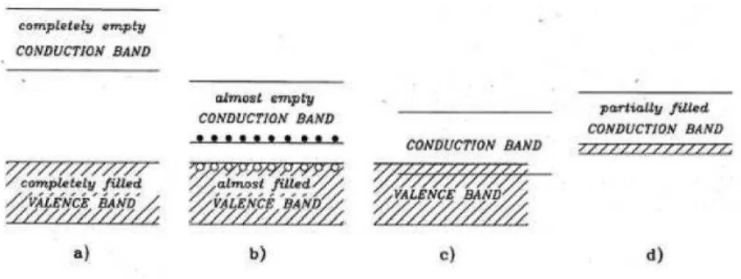
Solid energy bands are a set of energy levels accessible or not by the electrons within the lattice, and mainly result in two: the valence band and the conduction band. In Errore. L'origine riferimento non è stata trovata. we can see the possible situations of the bands in the insulators (a), in the Semiconductors (b) and conductors (c, d).
13
Figure 1-1 Model bands in solid state
One of the main reasons why semiconductors are used in electronics is due to the ability to modify their electronic properties in a highly controlled manner by adding small amounts of impurities called dopant, which can be classified into two types: those that provide an excess of electrons to the conduction band, and those that provide an excess of holes to the valence band. A semiconductor with excess electrons is called semiconductor n-type, while a semiconductor with an excess of gaps is called semiconductor p-type. The band structure is therefore modified and energy levels are introduced in the gap. Silicon and germanium are both tetravalent semiconductors and share their four valence electrons with the first four neighbors (Errore. L'origine riferimento non è stata trovata.Errore. L'origine riferimento non è stata trovata.(a)). The purpose of n-type doping is to produce excess electrons in the material. To understand how to do n-type doping, consider the case of silicon
14
(Si). The atoms of Si have four valence electrons, each of which is covalently linked to one of the four adjacent Si's atoms. If an atom with five valence electrons, as one of the group VA of the periodic table (i.e. phosphorus (P), Arsenic (As), or antimony (Sb)) is incorporated into the crystalline lattice instead of a Si atom, then that atom will have four covalent bonds and a non-covalently bonded electron. (Errore. L'origine riferimento non è stata trovata.(b)). This extra electron is only weakly bound to the atom and can easily be brought into the conduction band. Already at normal temperatures practically these electrons in the conduction band. Since the excitation of these electrons does not create holes in the valence band, the number of electrons in these materials is higher than that of the holes. In this case, electrons are the major charge carriers and gaps the minority carriers. Because the atoms to five outer electrons have an electron from "donate", these atoms are indicated with the name of atoms "donor". The purpose of p-type doping is to produce an excess of holes in the material. In the case of silicon, a trivalent atom, such as boron, replaces an atom of Si in the crystalline lattice. The result is that an electron of silicon is missing from one of the possible four covalent bonds. In this way, the atom dopant (boron) can accept an electron from the valence band to complete the fourth bond: this generates the formation of a gap. These dopants are called "acceptors". When a sufficiently large number of acceptor is added, the gaps become more numerous free electrons. Thus, the
15
gaps are the majority charge carriers, while electrons are the minority charge carriers in p-type materials. (Errore. L'origine riferimento non è stata trovata. (c)).
Figure 1-2 Three types of silicon: (a) intrinsic without impurities, (b) n-type silicon doped with phosphorus, (c) p-type silicon
doped with boron
1.2 Existing Doping Techniques
In this subsection, the common doping techniques, Ion Implantation (I.I) and plasma immersion ion implantation, diffusion based method, and Spin on Dopant (SOD), with the relative advantages and defects are described.
1.2.1 Ion implantation (II) and Plasma Immersion Ion implantation (PIII)
Ion implantation is the main semiconductor doping method since the 1970s6–8. Is a low-temperature process for injecting ions of any element into any solid material, resulting in desirable modification in its chemical, electrical, optical and mechanical
16
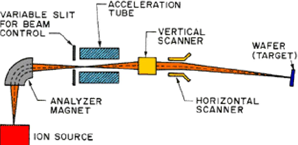
properties. For semiconductor applications, it is extensively used for selectively doping silicon wafers in precise control and for depth profiles of specific impurities. Operating at low temperature the lateral diffusion is negligible and is compatible with conventional lithographic processes, so small regions can be doped. Figure 1-3 Ion implantation systemshowed an Ion implantation system. In this system the precursor of the dopant wanted is introduced into the ionization chamber in which the free electrons, which are generated by thermionic effect, are accelerated under the influence of an electric field, by bombarding the molecules of the gas that is ionized by generating the desired ions.
Figure 1-3 Ion implantation system
The dopant ions irradiating the sample are accelerated with high energies ranging from a few tens of eV to the MeV. Using this type of doping, the maximum dopant concentration is found
17
within the semiconductor and the profile of the dopant distribution is mainly determined by the mass and energy of the implanted ions, the plant angle, the rigidity and the atomic density of the matrix undergoing the implant. In ion implantation, since the wafer surface is impacted by high energy ions, it can cause damage by knocking Si atoms from their position, causing local structural damage. This needs a post thermal annealing treatment to repair the damage.
There are two ways of doing this:
1. Tube furnace - low temperature annealing (600-1000 ◦C). To minimize lateral diffusion.
2. Rapid thermal annealing - higher temperatures are possible but for shorter times.
This technique shows a several issues:
Crystallographic damage: Each individual ion produces many point defects in the target crystal on the impact such as vacancies and interstitials.
Amorphization: The amount of crystallographic damage can be enough to completely amorphize the surface of the target.
Sputtering: Some of the collision events result in atoms being ejected (sputtered) from the surface, and thus ion implantation will slowly etch away a surface. The effect is only appreciable for very large doses.
18
Ion channeling: Crystallographic directions offer much lower stopping than other directions. The result is that the range of an ion can be much longer if the ion travels exactly along a particular direction. For this reason, most implantation is carried out a few degrees off-axis, where tiny alignment errors will have more predictable effects.
Plasma immersion ion implantation (PIII) 9–11is an upgrade of ion implantation technique in which the ions were extracted and accelerated from the plasma by applying a high voltage pulsed or pure DC power supply and targeting them into a suitable substrate or electrode with a semiconductor wafer placed over it, so as to implant it with suitable dopants. The electrode is a cathode for an electropositive plasma, while it is an anode for an electronegative plasma. Plasma can be generated in a suitably designed vacuum chamber with the help of various plasma sources. Figure 1-4 shows a PIII system. During the PIII process a component is immersed in a processing plasma discharge containing the desired species, and negative high-voltage pulses are applied directly to the component. Ions are extracted from the plasma and are implanted into the material’s surface.
19
Figure 1-4 Plasma immersion ion implantation system The ion beam current density depends both on the plasma parameters and the bias voltage and is of the order of 1 – 10 mA/cm2. A pulsed high voltage is used to reduce substrate heating as well as to control charging. Typical pulse lengths are in the range of 2 to 100 µs at frequencies of a few 100 Hz up to 3 kHz. The substrate temperature can be controlled by varying the implant parameters, and may range from room temperature to 600°C without additional heating. Self-regulating charge control achieved by the alternating attraction of ions and electrons enables one to process not only conductive, but also insulating surfaces. PIII technique has been developed in an effort to obtain increased ion current densities and to reduce both the implant time and the line-of-sight inherent to the conventional beam line ion implantation process. PIII efficiency is superior compared to the standard implantation process, particularly for Low-temperature
20
process, low energy, Less Hazardous System and high dose implants. Despite these advantages, this technique shows the following drawbacks:
- Possible unwanted impurities present in the plasma into the target can be implanted in addition to the desired dopants.
- Secondary electrons limit the efficiency and generate x-rays. - Limitation to check dose in situ
- Implant energy distribution is inhomogeneous.
1.2.2 Diffusion based methods
In the diffusion process semiconductor wafers are kept in a high temperature quartz tube furnace, and an appropriate gas mixture is passed.
Thermal diffusion is a two-step process:
1. Deposition - dopant atoms are introduced at the wafer surface. 2. Drive-in - the dopant atoms then diffuse into the wafer to create the required concentration gradient.
Boron is the most common p-type impurity in silicon, whereas arsenic and phosphorus are used extensively as n-type dopant. These three elements are highly soluble in silicon with solubility exceeding 5 x 10²⁰ atoms / cm3 in the diffusion temperature range (between 800° C and 1200° C). These dopants can be introduced via several means, including solid sources (BN for B, As2O3 for
21
As, and P2O5 for P), liquid sources (BBr3, AsCl3, and POCl3), and
gaseous sources (B2H6, AsH3, and PH3). For liquid and gaseous
sources, a concentration of the dopant vapor should be established at the surface. In a liquid source case, a carrier gas is usually used to transport the vapors to the diffusion furnace (e.g. N2) and is
then reduced at the surface. In solid sources case, wafer sized “slugs” are packed into the furnace along with the product wafers (e.g. for boron, boron nitride slugs can be used as solid sources), this is called a solid neighbor source. The number of dopant atoms diffusing in the wafer are proportional to the partial pressure of dopant impurity in the gas mixture. The doping concentration decreases monotonically from the surface, and the in-depth distribution of the dopant is determined mainly by the temperature and diffusion time12,13. The pros of this technique are: the lack of damage in the crystal lattice and can be used to batch fabrication. The cons related at this techniques are: Diffusion is bonded to solid solubility, the process needed high temperature, s difficult to create shallow junctions.
1.2.3 Spin on Dopant (SOD)
Spin-on dopants (SOD) provide an impurity source for semiconductor junction fabrication. This method permits a precise control of dopant entering the silicon through application of a homogeneous solution to the substrate using a spin coating method. In this process, no storage of source wafers or use of
22
costly ion implant equipment is used. After the film deposition over the substrate a diffusion step is performed at high temperature to yield desired sheet resistance and junction depth14–
16
. The cons of this technique are: diffusion of unwanted materials together the desired dopants, difficult to cover not-linear surface and like in the diffusion technique also this case suffer of the limitation to solid solubility and needed high temperature.
1.3 Molecular Doping (MD)
Recently an alternative, easy and low cost strategy to out match the standard doping methods has been proposed: the Molecular Doping (MD) 1. It is based on the interaction between a molecular precursor containing the dopant atom and the Si surface. The substrate is immersed in a solution containing the molecular precursor. After the deposition time, typically 2.5 hours, on the substrate surface a layer of molecules was formed, with a final surface density strictly correlated to the molecular footprint, i.e. through a self-limiting process 1. After this step the sample is covered by silicon oxide for protection and annealed in order to decompose the molecule and diffuse the dopant atoms inside Si, with kinetics driven by the diffusion phenomena. The MD is based on a process that involves the use of liquid precursors, this is an advantage which can be exploited for example in the doping of the nanostructures. MD can provide n- and p-type doping and a range of dopant doses, diffusion depths and resistivity controlled
23
by the molecular structure and design, the deposition conditions and the thermal budget 1,2,17–21. Metallurgical junctions as small as 5 nm and 10 nm have been demonstrated respectively for n+ and p+ doping, and electrical resistivity maps have shown that the wafer-scale uniformity bottle-neck is represented by the annealing process homogeneity22,23. The molecular precursor has been applied on planar, micro- and nano-structured surfaces and subjected to the diffusion thermal treatment 21,24–26 demonstrating the absence of crystal damage. The MD layer can also performed using a sacrificial target which is then put in contact with the substrate to be doped, in the so called contact doping method, where the molecules volatize upon annealing and then interact with Si in a fashion similar to the classic gas source methods 27,28.
24
2
Study of the interface between the
molecule and Si in MD
Silicon has undoubtedly been for decades the leading actor among the other semiconductor materials thanks to its abundance, stability and non-toxicity, and the projections confirm this supremacy also for the next years. In addition, the semiconductor roadmap miniaturization objectives are low cost and sustainable production. These have posed constraints for the doping process, i.e. the introduction of the dopant impurities into the intrinsic semiconductor with the function to modulate its electrical properties. Conventional doping methods (ion implantation or diffusion based method) present cost and safety issues, not to count the difficulty to obtain abrupt doping profiles, conformal doping, when the technology requires the dopant atoms to follow 3-D nano-structured surfaces, channelling, charging and crystal damage. MD was showed for the first time in 2008 as an alternative and low cost method in a work of professor Javey and his group1. Is based on the interaction between a molecular precursor containing the dopant atom and the Si surface. The substrate is immersed in a solution containing the molecular precursor for a typically deposition time of 2.5 hours and on the substrate surface a layer of molecules was formed. After this step, the sample is covered by silicon oxide for protection and annealed in order to decompose the molecule and diffuse the dopant atoms
25
inside Si, with kinetics driven by the diffusion phenomena. The MD is based on a process that involves the use of liquid precursors, this is an advantage which can be exploited for example in the doping of the nanostructures. MD can provide n- and p-type doping and a range of dopant doses, diffusion depths and resistivity controlled by the molecular structure and design, the deposition conditions and the thermal budget 1,2,17–21. MD has been applied on planar, micro- and nano-structured surfaces demonstrating the absence of crystal damage. The MD process can also performed using a sacrificial target which is then put in contact with the substrate to be doped, in the so called contact doping method. The interaction between the molecule and Si in the solution-based MD approach is the crucial point to be studied to deeply understand the mechanisms associated with the MD process.
In particular in this chapter, the following points are discussed in detail:
• study of the physics-chemical characteristics of the molecules in the standard synthesis conditions • study of the bond after different surface treatments
• study about the dependence of MD on the concentration of the molecular precursor in the solution.
26
2.1 Physical-chemist
characterization
of
the
molecules in the standard synthesis conditions
Semiconductor doping through solution-based self-assembling provides a simple, scalable, and cost-effective alternative to standard methods and additionally allows conformality on structured surfaces. Among the several solution-based deposition techniques, dip coating is the most promising. It consists in immersing the target to be doped inside a solution containing the dopant precursor. During this process, the molecule bonds to the target surface with a self-limiting process ruled by its steric properties. Successive annealing leads to layer decomposition and diffusion of dopant atoms inside the substrate. Most of the work on molecular doping lacks information on the molecule/Si interface chemical properties, on the mechanisms of the molecule evolution during the coating, and of its decomposition after the diffusion step. Moreover, it has so far been devoted to the molecules design to tune the final dopant dose and distribution. In this paragraph, new findings on the interface characteristics in terms of mono and multilayers formation are presented. A systematic study by varying the coating conditions was carried out, demonstrating that the main parameters such as carrier dose, junction depth and sheet resistance can be controlled precisely and that uniformity can be achieved at the nanometer level. 29,30. The substrate mostly used in this kind of process is Si 25,31–33 but
27
in literature are present work that involved the use of several substrates such as InAs, InGaAs oxidized silicon, alumina, and mica to study the molecule anchoring mechanisms 29,30,34,35. The dopant atoms typically injected in the MD are phosphorus, boron, sulfur and in recent work nitrogen arsenic or antimony was used too. The precursor source molecules are several. Octadecylphosphonic acid (OPA) molecules were deposited by dip coating 36–38 or drop casting 39 on a Si surface. In these work, the drop lateral diffusion over the surface during the days after the drop casting was studied by changing the substrate temperature. The result showed a surface redistribution of the molecules and it has been attributed to their amphiphilic nature 40. The authors found that the molecules were organized in bi- or multiple layers containing always an odd number of it (3,5,7. . .). This behavior is due to the polar nature of the molecules, bonded to the substrate thanks to the polar head, and with the nonpolar tails attached to the successive molecule. Another study on OPA molecules showed the important role of the solvent in the formation of self-assembled monolayers of OPA on oxide surfaces 40. Changing the solvent polarity, it is possible to determine a total coverage of OPA on substrate surface (using non-polar solvent) or not at all (using a polar solvent). Self-assembled monolayers OPA have also been obtained by T-BAG method on oxide-covered silicon samples 41,42. The characterization of this T-BAG process was performed by X-ray photoelectron spectroscopy (XPS) 41. A bulk
28
film of OPA is deposited after the T-BAG process, performed at room temperature and after baking at 140°C, the layer is converted to a multilayer, with a first one chemically bonded to the substrate and the rest only weakly bonded. The not chemically bonded multi layers are removed after rinsing and a total coverage of single monolayer is obtained after three cycles of deposition, baking, and rinsing. The identification of a tridentate bond between the P atom and three oxygen atoms is deduced from the single component of the P signal. All of these studies evidence the possibility of the formation of mono- or multilayers of molecules through MD, and this controls the amount of initial dose of dopant and of the final incorporated dopant in the substrate, and the importance of the synthesis conditions. In this part of my work, an experimental investigation of MD by focusing on the chemical surface properties and on the coating process conditions will be presented. The morphological and chemical characteristics of the as-deposited molecule and its interactions with the substrate are obtained by performing atomic force microscopy (AFM) and XPS with the goal to demonstrate the presence of the self-assembled monolayers and the molecule modification after the dip coating deposition and after the activation annealing.
The MD procedures found in literature usually start with the dipping of the samples in a 16% HF solution for 60 second to remove the native silicon oxide followed by immersion in 20%
29
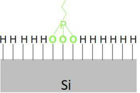
v/v solution of diethyl 1-propylphosphonate and mesitylene at the solution boiling temperature, about 160 °C, for 2.5 h 1,2,25,34. This step creates layers of phosphorus-containing molecules all over the sample surface (Figure 2-1a). In case of p-type doping, a boron precursor, such as the allylboronic acid pinacol ester (ABAPE), mixed in mesitylene is used at its boiling temperature of about 120 °C 24.
30
Figure 2-1 Schematic model representing the steps for the molecular doping based on the self-assembling coating process The samples, after the reaction, are immediately capped with a SiO2 layer deposited by spin on glass (SOG) procedure 2,24,25 (Figure 2-1b). In particular the samples after the molecular deposition have been baked at 80 °C for 60 s on a hot plate, and then covered by SOG oxide deposited by spin coating at 3000 rpm for 20 s. A subsequent baking step at 250 °C for 60 s in air and a last annealing step in the furnace to compact the SOG layer at 425 °C for 1h under 2l/min flow of N2 were then performed.
This process is indicated in the literature as a protection of the dopant molecules and the sample surface from air exposure and from the “escape” of the dopant during the subsequent activation annealing step. A furnace or RTA annealing at temperatures ranging between 900 and 1100 °C for times between 5 and 500 s is then performed to diffuse and activate the dopant (Figure 2-1c). The aspect related to the surface morphology after the deposition of the precursor molecules, especially in terms of formation of mono- or multilayers, has been investigated and debated in the literature. The results present so far, as discussed in the introduction, essentially show that the surface morphology strongly depends on the deposition methodology used. The morphology of the Si substrate after the molecules deposition has been tested also for the dip coating technique.
31
Figure 2-2 AFM micrographs of Si substrates after dip coating in the solution composed of the molecule and mesitylene (a) and
only the mesitylene (b). Map of the deposited layer in the region subjected to scratch test by AFM tip (c).
32
AFM maps have been acquired, by using a DI3100 atomic force microscope, on a sample “as-deposited” (Figure 2-2 a), i.e., after the coating process and without any further treatment such as deposition of the cap layer or annealing process. The topographical map shows that, besides a small roughness that can be correlated to the deposited molecules circular agglomerates with variable size are present. To attribute the presence of the agglomerates to the molecules or to possible other contaminants, such as solvent residuals or decomposition products, AFM measurements were performed on samples immersed in a solution containing only the solvent and by using the same coating conditions. The data are shown in Figure 2-2 b and as can be seen also, in this case, the agglomerates are present while the roughness has disappeared. So, it is possible to attribute their presence to some solvent residuals. This can be expected since the solvent used presents a degree of purity of 98 %. Electronic grade chemicals should be used to overcome this issue. To investigate the thickness of the deposited layer, a scratch with the AFM tip was performed by impressing a force onto the surface by the movement of the AFM tip in contact mode on a restricted area of the sample (Figure 2-2 c). The height of the step formed, corresponding to the thickness of the deposited layer, was measured and resulted in being less than 2 nm, which coincides with the value of the expected thickness of a monolayer of diethyl-1-propylphosphonate 43. To further investigate the
33
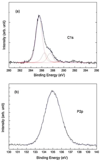
formation of the self-assembled monolayer and its chemical bonding with the substrate, XPS measurements on the as-deposited samples with a base pressure of 2×10⁻¹⁰ torr were performed. A monochromatic Al Ka radiation was employed as the excitation source. XPS spectra at 108 photoelectron angles (relative to the sample surface) were collected, to increase the surface sensitivity of the analysis. In Figure 2-3, the spectra of the C1s (a) and P2p (b) are displayed. The C1s spectra can be deconvoluted in 4 components: the main peak is centered at about 285.4 eV and is attributed to the presence of monolayers chemically bonded to the Si surface 41, a second component at higher binding energy, 286.5 eV, indicate the presence of some residual non-chemically bonded multilayers, while the peaks at 287.5 and 289 eV are attributed to oxidation species such as C–O and C=O, respectively. Figure 2-3 b shows that the P2p signal is constituted by a single component centered at 135 eV. The literature data reports the signal for not oxidized P species at 130 eV 44,45, while our experimental peak position indicates that the P is bonded to an electronegative atom in this case oxygen. It is possible to propose a hypothesis for the anchoring of the molecule. In fact, observing the P2p peak, it is symmetrical. The fact that the peak is symmetric indicates that it consists of a single contribution and suggests that there is only one type of bond between O and P, presumably due to the breakup of the double bond P = O and the simultaneous breaking of the C-O-P bonds. In
34
the literature, a tridentate model for similar molecules is proposed
41
. If so, the aliphatic portion of the molecule detaches during the coating process, forming some compounds, and the remainder of the phosphorus molecule is bound via oxygen to the substrate.
Figure 2-3 XPS spectra relative to the C1s (a) and to the P2p (b) signals acquired on the as-deposited sample.
To investigate the decomposition of the molecule, Raman analysis in the as-deposited samples and after the activation step has been
35
performed. The relative spectra are shown in Fig. 4. The results display vibrational features in two well different regions: the first one, between 1000 and 1500 cm-1, associated to the deformations of methylene (CH2) chain and to terminal methyl (CH3), and the
second one in the wavelength region of 2800–3000 cm-1 where symmetric and asymmetric stretching modes of the CH2 and CH3
units are visible. Note that unfortunately deformations, twisting and rocking modes of alkyl groups overlap the P=O and P–O– C2H5 vibrational bands which fall between 1000 and 1300 cm-1.
Therefore, it was not possible to evidence the molecule structural changes after anchoring to the Si substrate by exploiting vibrational features of phosphorus containing groups. Moreover, at higher frequencies four prominent bands can be assigned to the C–H stretching modes of the CH2 and CH3 groups. In the
as-deposited sample (red curve), the symmetric and asymmetric stretching modes of the methylene groups are positioned, respectively, at 2846 and 2912 cm-1, while the symmetric and anti-symmetric stretching modes of the methyl groups were observed at 2879 and 2958 cm-1, respectively. After the high-temperature thermal treatment, i.e., the activation step (black curve), CH2 stretching mode shifts in the positions toward higher
frequency while CH3 remains almost invariant. Moreover, a
change of overall relative intensities was also observed. The CH2
stretching modes in the alkyl chains are conformational order dependent shifting to higher frequencies at higher conformational
36
disorder 38–40. In addition, a mode at 1735 cm-1 was observed in both samples. This frequency is correlated to the stretching vibration of C=O of alkyl propionates species, so we can hypothesize that during the 150 °C dip coating process, a partial pyrolysis takes place leading to a transformation of the diethyl propyl phosphonate. Such compounds might be associated with the transformation of the aliphatic portion of the molecule detached during the dip coating, observed during the XPS analysis. If the appearance of the C=O bond induces to speculate a partial pyrolysis of the molecule during the dip coating process, during the activation step this phenomenon further proceeds, as demonstrated by the frequency shifts and by the relative intensity variation of the CH stretching modes in the range of 2800–3000 cm-1.
37
Figure 2-4 Raman spectra acquired on the as deposited sample (red line) and after the activation step in furnace at 1050 °C for
500 s in N2 (black line).
The results of the Raman analysis confirm the results obtained by XPS analysis on the fresh sample, indicating that the molecule starts to break and loss the lateral aliphatic chains during the coating process.
Figure 2-5 Hypothesis of a possible bond between the DPP and Silicon substrate
Figure 2-5 shows a hypothesis of the possible bond between the DPP molecule and the silicon substrate. From the results obtained by the XPS and Raman analysis and from the literature works it is possible to hypothesize that the molecule during the deposition process form a tridentate type bond with the substrate. In particular the dopant atom is bonded to the substrate via oxygen following simultaneous rupture of the C-O-P and the P = O bonds.
39
2.2 Role of the surface treatments
In the previous section it was found that during the deposition process for MD there is the formation of both the monolayer chemically bonded to the substrate and of the multilayers physically linked to it. In order to obtain more control on the MD process, it is important to limit the formation of the layers physically bonded to the substrate or removing them subsequently. For this reason, a series of experiments have been conducted in these two directions to remove or restrict the formation of the physi-sorbed layers.
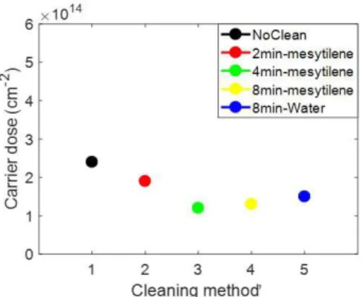
In the literature, a study on TBAG and the possibility of removing the fused adsorbents by THF was performed with the focus of identifying multilayer vs. monolayer films 41 In MD process cleaning was applied for the first time in a work of 201118 in which authors removed the physi-sorbed material by rinsing the sample in ethanol, acetone, and MilliQ water and then ultrasonicated it for 15 min in acetone. In this work, no experimental evidence about the role of the cleaning on MD are present. For this reason, different cleanings were performed on the samples to fine-tune an effective removal method. Preliminary tests of cleaning in mesitylene, with increasing times from 2 minutes to 8 minutes and in water for 8 minutes were carried out. Then the samples were annealed at 1050°C for 500s and characterized by SRP to obtain an electrical measurement that can
40
be correlated to an indirect indication about the removal physi-sorbed materials. In Figure 2-6 the dose value of the samples rinsed in water and mesitylene has been plotted.
Figure 2-6 Dose obtained from SRP profiles after annealing of standard samples (no clean) and cleaned in mesitylene or water
at various times.
The samples after the cleaning processes were observed with an optical microscope in order to detect the possible presence of macroaggregates (images not shown). Samples cleaned with mesitylene showed the presence of aggregates on the surface, probably due to the presence of contaminants in the solvent itself. Samples cleaned with water did not show the presence of this aggregates and for this reason it was chosen as one of the cleaning methods preferring it to the one in mesitylene. In addition to this, another method chosen was that already present in the literature and used in the MD and it consists in rinsing the sample in
41
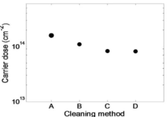
ethanol, acetone, and MilliQ water and then ultrasonicated it for 15 min in acetone. Finally, the last method presents in literature where the sonication cleaning was substituted with magnetic stirring. So the samples for found a better method to remove the physi-sorbed layers were prepared in the following way: No cleaning (A), cleaning in ethanol, acetone, MilliQ water and then sonicated in acetone for 15 min (B) , cleaning in water through magnetic stirrer (C) and cleaning in acetone, isopropanol, water and 15 min in acetone under magnetic stirrer (D). After the cleaning the samples, also in this case, were annealed at 1050°C for 500s and characterized by SRP. In Figure 2-7 it is possible to note how the most effective removal method of the layers not chemically bonded to the substrate is the D case that undergone the samples to magnetic stirring.
Figure 2-7 shows the plot of dose values, calculated from SRP profiles, of the various samples: no cleaning (A), cleaning in
42
cleaning with water using magnetic stirrer (C) and cleaning in acetone, isopropanol and water and then in acetone under
magnetic stirrer (D).
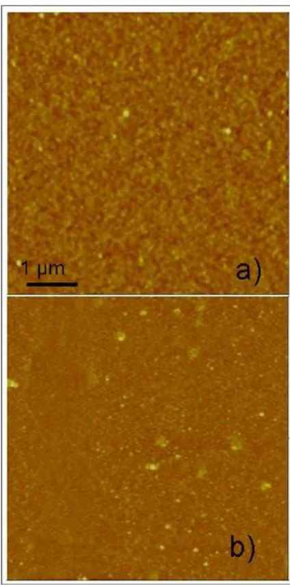
Once the most effective removal method was found, this was chosen as a removal method for the morphological characterization of the samples. A second step was to analyze the morphological characteristic of the cleaned samples and compared it with the no cleaned samples. For this reason, the “as deposited" samples, after the cleaning cycle, was immediately characterized by morphological point of view through AFM to have an indication about the removal of the non-chemically bonded layers. In Figure 2-8 AFM microscopes are shown. The RMS was calculated for both samples to have an index of the roughness of the surface before and after the removal treatment. In Figure 2-8 a) the RMS value was of 0.740 nm while for the samples in Figure 2-8 b) the value was 0.374 nm. The RMS value in the case of the cleaned sample is considerably lower (about half), suggesting an effective removal of the physi-sorbed layers.
43
Figure 2-8 AFM micrograph of the samples no clean (a) and cleaned with acetone, isopropanol, water and acetone under
magnetic stirrer (b)
The no-cleaned sample shows a total coverage of the substrate but there is the appearance of aggregates of the order of a few hundred nm. The presence of these aggregate could be caused by an increase of dopant concentration during the coating process due to the different boiling temperature between solvent and DPP. Indeed, the boiling temperature of mesitylene is about 160 °C while that of the DPP is about 280 °C. This could lead to formation of dopant aggregates on the surface during the process.
44
2.3 Role of the dilution of the precursor solution
In order to investigate the presence of the aggregates described in the previous paragragh a further approach consisted to decrease the concentration of DPP in mesitylene at 20,10 and 5% respectively. In this case, a systematic study was performed both morphologically and electrically at various concentrations.
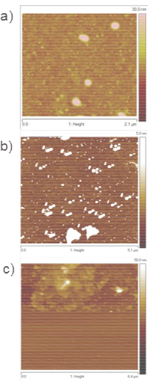
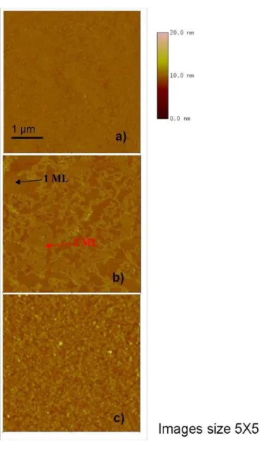
The AFM images are shown in Figure 2-9 and it is seen that the surface roughness increases from the sample to 5% to 20% respectively. Specifically, the 5% sample has a Root Mean Square (RMS) of 0.250 nm. This value doubled in the case of the 10% sample (RMS 0.500 nm). Also in this sample, it is possible to note the presence of "voids" during the formation of the monolayer. The RMS value in the "voids" is different from the silicon value (0.130 nm) but very like the measured value for the sample at 5% (0.230 nm) indicating the presence of a layer already formed and that of a second layer in formation. In this case the vertical distance of the second layer was measured and the results show how the distance between the two layers is about 1 nm. In the third case, RMS was 0.740 nm. In this case there are no terraces indicating a total coverage of the substrate but there is the appearance of circular shaped aggregates the order of the hundred nm. Results from AFM images show a strong evidence about the role that DPP concentration plays in monolayer formation.
45
Figure 2-9 AFM microscopies carried out on samples, varying the concentration of the DPP a) 5%, b) 10% and c) 20% Successively a set of samples processed in the same manner was characterized by SRP in order to understand the possible differences in terms of dose between the samples. Figure 2-10
46
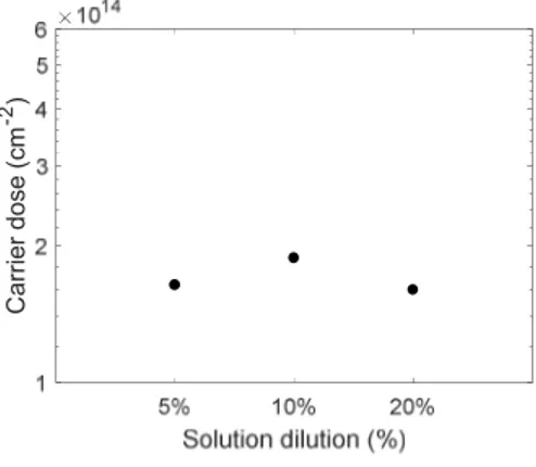
shows how the dose values, calculated from the SRP profiles, are similar in the range of 5 % and 20 %, while the value of the samples at 10 % is higher. Probably because of the formation of 2nd layer that was found in AFM images. In this case the lack of formation of macromolecular aggregates allows better adhesion of the molecule to the substrate and consequently to a higher dose.
C a rr ie r d o s e ( c m -2)
Figure 2-10 Carrier Dose value obtained by SRP profiles of the samples at various diluition of DPP
Finally, to study the removal of the physically bonded layers to vary the concentration of the molecular precursor, 2 sets of samples were prepared. The first set was prepared as deposited, cleaned with acetone, alcohol and water and then again in acetone using a magnetic stirrer and then morphologically analyzed using AFM. The second set of samples, equal to the one being analyzed AFM, was annealed after the cleaning process to get feedback from the electrical point of view. Figure 2-11 show the AFM
47
micrograph obtained for the cleaned samples at 5% (a), 10% (b) and 20% (c) dilution of DPP in mesitylene solution.
Figure 2-11 AFM microscopies carried out on "cleaned" samples, varying the concentration of the DPP a) 5%, b) 10%
48
In the first case of the sample after treatment the RMS has the same value as that of the 5% untreated sample (0.250 nm). In the second case, it becomes apparent that cleaning is effective in removing the layers physically bonded, there are no terraces indicating a total coverage of the substrate and the RMS value is equal to 5% (0.250 nm). Finally, in the third case the RMS has a value of 0.374 nm which is about half compared to that of the untreated samples. Results from AFM images strongly suggest the role that the concentration of DPP plays in the formation of the monolayer and that the subsequent dip coating treatment removes the physically attached layers. Then the second set of samples was prepared as the previous case but was annealed a 1050°C for 500 s to obtain an indirect indication about the removal of physi-sorbed layers.
Figure 2-12 Carrier dose obtained by SRP profiles of the samples at various dilution of DPP and cleaned with acetone, alcohol and water and then again in acetone using a magnetic stirrer
49
Figure 2-12 show the carrier dose of the annealed samples after the MD and cleaning. In this case the value of samples at 5% and 10% was comparable and this trend confirmed the result obtained by the AFM micrograph and both cases showed a higher value than the sample at 20. This trend is due to the contribution of 2 phenomena: the first is the formation of macromolecules during the deposition phase which does not allow the best adhesion of the molecules and the second is the subsequent evaporation of the molecules itself during the annealing process.
50
3
Role of the deposition parameters
This chapter discusses about the role of the main deposition parameters in MD technique. The ability to modulate the main parameters corresponds to have a control over the MD deposition technique and then to have an ability to design and to prepare a sample with the desired characteristics.
In the first part of this chapter the role of coating time and sampling time will be reported. In the second part, the role of the solvent and the molecular precursor will be discussed.
3.1 Role of the coating time and sampling time
The literature on the MD doping technique shows that it is possible to modify and control the doping profile by changing the molecule design. Specifically, the molecular footprint of the precursor directly governs the surface concentration of the dopants with larger molecules resulting in a lower dose 1,34. Starting from the results obtained in the previous chapter, where the samples show the presence of multilayers physiosorbed on the surface, a further approach was to change the immersion time of the samples in the precursor solution. For this reason, the samples were dipped first in a HF solution to remove the native oxide layer and then in a 20% v/v of DPP in mesitylene solution from 5 to 150 min. In Figure 3-1 a, the results of the SRP profiles are reported as carrier concentration versus depth for the several
51
coating times, all activated at 1050 °C for 500 s. As it is possible to see the profiles show a continuous increment in the junction depth until a saturation is obtained for the 100–150 min coating time. Figure 3-1 b and c show, respectively, the carrier dose and the junction depth calculated from the SRP profiles, as a function of the coating time. The trend of the charge carrier concentration and of the junction depth, as a function of dip-coating time, is monotonous. From the obtained data, it can be stated that the concentration of charge carriers and the junction depth can be precisely controlled by varying the time of coating. The results discussed above led to ask how thermal activation time affects the carrier concentration and the junction depth.
52
Figure 3-1 (a) Carrier concentration profiles as a function of the depth for several dip-coating times, carrier dose (b) and
53
Thenthe variation of DPP concentration during the process and if this variation can be responsible for the formation of the agglomerates described in the previous chapter (see Figure 2-11) is investigated. In this case the dilution is not changed by purpose but is modified during the process due to the evaporation of the solvent. For this reason, an experimental set up was carried out by processing 3 different types of samples. The samples were divided in two group for AFM and SRP characterization. All the samples were immersed in HF for the removal of native oxide and then were inserted for 25 min each, two samples were inserted at time = 0 min until time = 25 min, other two samples from time 50 min to time 75 min and finally the third group of samples was inserted at 125 min up to 150 min. One sample of each group was analyzed morphologically via AFM. (Figure 3-2) and the other one was annealed at 1050°c for 500s and then characterized by SRP. By comparing the three images (Figure 3-2 a, b and c), the formation of aggregates becomes a evident phenomenon only in the latter. This trend is even more clear by comparing the RMS numeric values: in case a) the value is 0.25 nm, in case b) it has a value of 0.550 nm while in the last case (c) the value is 0.970 nm. This phenomenon may be due to an increase in the concentration of DPP in the solution due to solvent evaporation at increasing dip coating time and consequently to its aggregation in macro-micelles depositing on the substrate.
54
Figure 3-2 AFM micrograph performed on samples processed for the same duration of 25 min but inserted at later times in
55
Figure 3-3 shows the carrier dose obtained by SRP characterization of the sample immersed at different time. As can be seen, the carrier dose changes in the 3 samples. This indicates that the concentration of solution changes during the process. In particular, the trend is decreasing and this indicates a decreased ability of the molecules to adhere to the substrate surface. This result fits with those obtained through morphological analysis where we saw the appearance of macro aggregates in the sample immersed for last. These macroaggregates seem to be formed by dopant precursors, which due to micellar assembly, fail to form chemical bonds with the surface and bind to this through weak physical bonds.
Figure 3-3 Carrier Dose from the SRP characterization of the sample after different immersion times
56
3.2 Role of the solvent and the molecular
precursor
Another aspect investigated in this thesis was the role of the solvent and the molecular precursor at the MD. In the literature, an aspect not yet investigated concerns the variation of solvent in this type of processes. For this reason, a first aspect investigated was to replace the common solvent used in MD, mesitylene, which is an organic solvent, potentially toxic for fish and polluting for marine environments. The solvent selected to replace mesitylene should have the following characteristics: non-toxic, non-polluting, easily available, cheap, carbon-free: For this reason, we explored water as a solvent for the DPP.
Samples of Si p type with <111> crystallographic orientation was processed by MD after a brief dipping in a 16% HF solution for 60 second to remove the native oxide. After the samples were immersed in a 20% solution of DPP in water at its boiling temperature, about 120 °C for 2.5h. Then one sample before the activation thermal step was cleaned in acetone isopropanol and water and then in acetone under magnetic stirrer and finally all the samples were annealed at 1050°C for 500s. After the activation process the samples were characterized by SRP in order to obtain information about the electrical properties. Figure 3-4 shows the Carrier dose of the samples at different dilution in mesitylene (described below) cleaned or not cleaned and compared with the
57
samples processed using water as a solvent and also in this case undergone or not at the cleaning process.
Figure 3-4 Carrier dose of the samples at different dilution in mesitylene: no cleaned (black dot), cleaned(red dot), and in
water: no cleaned (black square) and cleaned (red square) In the case of no cleaned sample the dose value is 5.3 13 while in the case of the cleaned sample is 2.9 12. The value of the sample no cleaned compared to the conventional MD is about half while it is about 2 orders of inferior magnitude in the case of the cleaned sample. The cause can be attributed to the formation of a layer of oxide at the interface between the solution and the substrate before the molecule binds to this. This oxide layer limits the diffusion of molecules due to the different diffusion coefficient.
A second aspect was related to the necessity to not introduce unwanted contaminants inside the substrate during the annealing
58
process. In literature, any works are focused on the use of further molecular precursor but in all cases, the molecular precursors used were complex molecules in which the ratio of carbon/dopant atoms was higher than in DPP precursor20,46. For this reason, an innovative molecular precursor was choice to reduce the carbon atoms constituting the molecular precursor to zero. Phosphoric acid (PA) was chosen because his molecular structure is composed only of oxygen, hydrogen and phosphorus, no carbon atom is present. Also in this case, like the DPP, the phosphorus is bonded to an oxygen atom through a double bond. It is known in microelectronics because it is used in the removal of silicon nitride but which has not been, until now, as a dopant. In this case, the samples were cleaned in the following manner. Firstly, were sonicated for 5 minutes in acetone, then for 5 min in alcohol and finally for 5 min in water to remove the physical contaminants. Successively were dipped in HF solution, and then immersed in a 20% solution of Phosphoric Acid in water at 120°C for 2.5 h. Then the samples were annealed at 1050°C for 500s and then characterized by SRP. Figure 3-5 show the SRP profiles of the samples doped by Phosphoric Acid.
59
Figure 3-5 SRP profiles of samples doped by Phosphoric Acid In this case the dose is about 6.5×10¹⁵ at/cm2 and the junction depth reaches more than 1.4 microns. The differences are remarkable by comparing these samples with those doped with DPP in mesitylene (Figure 3-6).
Figure 3-6 Carrier dose calculated of the samples doped by PA and DPP
60
Indeed, in this case the dose values are more than one order of magnitude greater, the junction depth values are about 5-6 times larger and the Rs is less than one order of magnitude. Moreover, as can be seen in the Figure 3-6, the samples doped with phosphoric acid have a lower error bar than DPP-doped samples. In order to investigate whether the spreading length of charge carriers observed in doped samples with PA can be modulated through the annealing time, a second process was performed by changing the annealing time from 500 s to 20 s. Also in this case the samples were characterized by SRP and the profiles were reported in Figure 3-7.
Figure 3-7 SRP profile of the samples doped by Phosphoric Acid and annealed at 1050°C for 20s.
In this case, the profiles obtained are slightly different from those scored for 500s. In fact, the dose is about half that obtained in the previous case (3×10¹⁵), as well as the Rs (about 20 ohm / sq) and also the junction depth value is less (about 1 micron). Despite the
61
same processing conditions (temperature, time and ambient), different dose, sheet resistance and diffusion lengths have been observed compared the samples doped by PA and the samples doped by DPP. These differences could be ascribed both to the change of the molecular precursor, anomalous diffusion effects and/or to the nonlinear diffusivity at high concentrations. In order to get a qualitatively frame of the data the ideal theoretical diffusion length was evaluated (Figure 3-8 red line and dots) using the following equation:
L= 2Dxt (Eq.1)
using the extrinsic non-linear diffusion coefficient of P in Si:
Dx = D0+D- -(n/ni)2 (Eq. 2)
where D0 = 3.85 e – 3.66/kT, D-- = 44.2 e -4.37/kT, where n is
approximately evaluated as the maximum carrier concentration peak in the SRP profiles and ni is the carrier concentration of
62
Figure 3-8 Sheet resistance results obtained by the SRP profiles as a function of the sample annealed both at 1050°C for a) 500s
and b) 20s, in red the calculated diffusion length
The comparison in Figure 3-8 demonstrates that the qualitative trend of the junction depths for the different cases is remarkable. The causes could be due to several factors: first, the different dimensions of the phosphoric acid molecule compared to the DPP, second point is correlated to the concentration of molecular precursor in solution, indeed the solution was prepared using the same volume percentage of the DPP case, but in this case the number of molecules present in the solution is about 3 times greater. Finally, a further contribution probably due to the Si surface oxidation during the MD deposition and also during the annealing process, in spite to the nominally inert annealing conditions. The oxidation in fact produces a super-saturation of interstitial defects within the substrate that is responsible for a greater diffusion length [11-12].
63
4
Effects of the post-deposition treatments
This chapter shows the effects of the post deposition thermal process in MD.
In particular the chapter is divided in 3 parts: in the first one the role of the annealing parameters with particular attention on temperature and time was performed, in a second part an investigation about the chemical-physical properties on the surface of silicon samples after doping through molecular doping (MD) method and successive annealing is carried out. Furthermore, a study about the atomic structure of the first layers of silicon after the doping procedure in order to evaluate the possible intermixing between the carbon atoms constituting the precursor molecule and the Si atoms of the substrate is performed. Moreover, the role of this intermixed layer on the electrical characteristics of the semiconductor is also studied.
In the third part of the chapter the role on the cap layer on the MD process is discussed.