ALMA MATER STUDIORUM - UNIVERSITÀ DI
BOLOGNA
FACOLTÀ DI INGEGNERIA
CORSO DI LAUREA IN INGEGNERIA DELLE TELECOMUNICAZIONI
DIPARTIMENTO DI ELETTRONICA, INFORMATICA E SISTEMISTICA
TESI DI LAUREA in
Sistemi a Portante Ottica
CONTROLLO OTTICO AUTOMATIZZATO DI
CIRCUITI FOTONICI INTEGRATI:
PROGETTAZIONE, REALIZZAZIONE E
VALUTAZIONE
CANDIDATO: Federico Forni
RELATORE: Prof. Giovanni Tartarini CORRELATORI: Prof. Kevin A. Williams Dr. Ripalta Stabile
Anno Accademico 2012/13 Sessione III
Homo faber ipsius fortunae
Abstract
Nei prossimi anni le reti di telecomunicazioni dovranno affrontare un dra-stico aumento del traffico dati. L’attuale trasmissione su fibra ottica, con commutazione a pacchetto effettuata tramite switch elettronici, non potrà sopperire a tale incremento. Una soluzione promettente è la commutazione di pacchetto ottica, in cui la funzione di instradamento è svolta da circuiti fo-tonici integrati (Photonic Integrated Circuits, PICs). Le funzionalità dei PIC sono notevolmente aumentate negli ultimi anni. Tuttavia, la complessità e la lentezza della verifica delle funzionalità ottiche ne limita lo sviluppo: sono quindi necessarie procedure di controllo affidabili, veloci ed economiche. Nel progetto di tesi che viene di seguito presentato, è stata ideata, realizzata e valutata una procedura innovativa di verifica automatizzata delle funziona-lità ottiche dei circuiti fotonici integrati. Partendo dall’analisi delle criticità delle procedure attuali, sono state individuate le seguenti specifiche da re-alizzare come obiettivo: automatizzazione, flessibilità, affidabilità, semplifi-cazione dell’allineamento e velocizzazione delle operazioni di misura. Il banco di misura si compone di una griglia di microlenti, una matrice di fotodiodi e due programmi di controllo, acquisizione e analisi dei dati. I componenti sono stati studiati e calibrati, attraverso numerose prove che ne hanno deter-minato le caratteristiche. I due programmi sono stati sviluppati allo scopo di controllare l’intero banco di misura, dal PIC, al ricevitore, effettuando infine un’analisi dei dati. L’affidabilità del nuovo banco di prova è stata verificata con successo con riferimento ad un prototipo di PIC a 16 porte, del quale sono state analizzate: la posizione dei fasci, le curve corrente-potenza, la distribuzione spazio-temporale della potenza e la continuità ottica da porta a porta. Inoltre, sono state analizzate la precisione e la complessità delle operazioni di allineamento, dimostrando affidabilità e flessibilità inalterate a fronte di una drastica riduzione dei tempi di effettuazione delle misure.
Contents
1 Introduction 1
2 Concept 5
3 Test-bed setup and components 7
3.1 Photonic integrated switch . . . 7
3.1.1 Mechanical and optical requirements . . . 8
3.1.2 Photonic integrated switch prototype . . . 8
3.2 Microlens array . . . 12
3.2.1 Divergent multiple beams . . . 12
3.2.2 Linear lens array . . . 13
3.3 Optical receiver . . . 19
3.3.1 Photodiode array . . . 20
3.3.2 Interface board . . . 22
3.3.3 Tests . . . 24
3.4 Software . . . 34
3.4.1 Data displayer software . . . 35
3.4.2 Test controller software . . . 38
3.4.3 Data analysis . . . 44 4 Test-bed assessment 47 4.1 Preliminary operations . . . 47 4.2 Waveguide characterization . . . 51 4.2.1 Waveguide positions . . . 53 vii
4.2.2 Current versus power characteristic . . . 55
4.3 Optical continuity test . . . 56
4.3.1 Optical path structure . . . 56
4.3.2 Working point survey . . . 59
4.3.3 Optical path continuity . . . 62
4.4 Test performances . . . 66
5 Discussion 69 5.1 Spatial resolution . . . 69
5.2 Waveguide positions . . . 70
5.3 Microlens array tilt . . . 71
5.4 Current versus power characteristic . . . 71
5.5 Optical continuity . . . 72
6 Conclusion and outlook 73
Appendices 77
I Component Datasheets 77
II Calculations and demonstrations 99
III Eindhoven University of Technology final paper 103
Chapter 1
Introduction
Since the beginning of the new millennium, the telecommunications have faced one of the most significant challenges [1]. The Internet and the social networks have changed the technological trends faster than ever [2]. The network services have drastically increased their subscribers and coverage. As shown in Figure 1.1, the machine-to-machine (M2M) applications, high definition video playing [4] and wi-fi spots have dealt with an impressive growth in demand, providing greater data traffic than ever before. Every subscriber wants to be connected everywhere: therefore, large coverage, high mobility and on-line connectivity have become ubiquitous requirements for the wireless networks.
The futurable services and paradigms, e.g. the Internet of Things [5], are stressing these requirements: data traffic models provide an increasing band-width demand during the next decade, with an approximate doubling every year [6], [7].
The integration of optical fibre and wireless networks have become an essential technology for the provision of access to broadband wireless links [8], [9]. Its uses include last-mile solutions, improvement of radio coverage and capacity and backhaul of current and next-generation wireless networks. As long as the optical fiber medium is future-proof, since its current bit
Figure 1.1. Technological trends between the 2011 and 2015: percentage growth and users (users in 2011 → users in 2015) [3].
rate is conservatively estimated to be 1T b/s over a single fiber and with thou-sand kilometres between regenerators. As a consequence of this scenario, the pressure on transport network nodes is increasing [10], [11]. Indeed, they perform the routing and switching functions in the electrical domain: cur-rent routers redirect each optical channel, i.e. wavelength, to an ingress line card where the optical signal is converted to the electrical domain. Once the control information, as destination and priority, is retrieved, the data is processed and up converted again to the optical domain.
The transformation to the electrical domain in the intermediate nodes in-volves great limitations. The electronics speed is limited to 40Gb/s: conse-quently, the speed limitation generates a bottleneck incapable of absorbing the traffic throughput coming from the optical fibers. Additionally, the pro-cessing time in the electrical domain adds extra latency to the end-to-end communication. On the other hand, the optics-electronics-optics (O-E-O) conversion equipment augments decisively the intermediate node cost [12],
3
[13].
A promising solution is represented by all-optical networks: the inter-mediate O-E-O transformations are avoided and the signals remain in the optical domain from end-to-end.
Techniques providing optical circuit-switched network are the only solutions deployed [14]. Although, another technology is under research: the optical packet switching network [15]. It represents a very promising solution for next generation all-optical networks [16]: such a network would be able to offer virtual circuit or datagram services [17], [18], much like what is provided by IP networks, using photonic integrated switches [19].
The COBRA Research Institute of Eindhoven University of Technology has recently set the world-record for routing 320 Gb/s in a multi-stage optical integrated switch [20]. The complexity of state-of-the-art integrated chips is keeping growing: the number of components per chip reaches now hundreds [21], [22]. Nevertheless, the fast photonic integrated switch technology is not yet fully competitive with the electronic counterpart [18]. One of the greater limitations is the test complexity, which increases the analysis time and cost. Since the ’70 the automated test methods for electronic integrated circuits have been demonstrated to be solid and standardized procedures [23]. These reliable techniques have been exploited to provide hundreds of connections at one go.
Photonic integrated chips (PICs) will be competitive with electronic technol-ogy if a fast and reliable test procedure is developed. Photonic integrated switch facets integrity, as well as electrical connections quality after bond-ing, have been shown by visual inspection and automated electrical tests [24]. However, the optical test of these sophisticated chips is still very slow and complex.
In this master thesis project an automated test-bed for reliable optical assessment is conceived and provided, in order to hasten the photonic inte-grated circuit optical test. The thesis framework is reported below:
1. the current optical test problems and the project requirements are anal-ysed in chapter 2;
2. the selection and the test of the components and the assembly of the test-bed is described in chapter 3;
3. the verification of the test-bed optical test capabilities, performed by flip chip bounded photonic integrated switch trials is reported in chap-ter 4;
4. the critical problems observed during the assembly and assessment are discussed and solutions are proposed in chapter 5;
Chapter 2
Concept
The photonic integrated switch optical tests, which constitute the core of this master thesis work, are based on beam reception by fiber lenses. These are placed and aligned toward the waveguides. Therefore, the beams are collected and the data are processed by the receiver.
The critical problems are represented by the setup time and procedure com-plexity. The alignment requires strict placement tolerances due to the dis-tance between the devices, which is 10µm [25]. Consequently, all the device placements must be performed by microscope visual inspection in order to avoid the optical lens collision into the photonic waveguide. Moreover, the alignment precision is ' 100nm: this requires that all the fiber lenses are placed one at a time and the position must be corrected every hour in order to balance the chip thermal drift. Therefore, the test-bed set-up time de-pends on the number of fiber lenses positioned.
The other time-consuming step is the photonic integrated switch control because the test inputs are provided by manual input due to the lack of au-tomated test controller.
The test setup time, for the 16 × 16 ports PIC, is conservatively estimated in 4 months.
The envisaged test-bed should reduce the time-consumption related to 5
the setup and to the trial stages. The first step should decrease the time necessary for obtaining the photonic integrated circuit alignment toward the optical receiver and, to this purpose, it is desirable to relax the positioning precision. Moreover, it should simplify the placement complexity, avoiding the microscope visual inspection and introducing more practical feedback tools for the operator.
Furthermore, the trial step must also be time optimized: the test-bed should be able to perform multiple waveguide assessments in the same test and the operator intervention should be limited due to the increase of the test-bed automation.
Finally, the test-bed should be as layout independent as possible, reducing the test-bed changes necessary to test different waveguides and PICs, achiev-ing lower setup time.
These concepts drive to the envisaged automated optical test, which must satisfy few fundamental requirements to make it valuable for effective opti-cal test of sophisticate photonic integrated circuits. The specifications are following:
1. relaxed precision and still reliable alignment; 2. multiple port assessments at the same time; 3. independence from the chip layout;
4. real-time alignment and measurements; 5. high automation via software control;
Chapter 3
Test-bed setup and components
In this chapter the selection of the components for the test-bed is illus-trated.Each device is studied in 3 stages: firstly, its requirements are defined, sec-ondly, a comparison between different choices is made and, finally, the com-ponent performances are analysed with proper test-bed.
The methodology used is a bottom up approach: the project requirements are analysed starting from the photonic integrated circuit and its control, then the best available solution to carry the optic beam toward a theoretical optical receiver is studied. Subsequently the best optical receiver is defined and, finally, the data process and test control algorithms are programmed and optimized.
3.1
Photonic integrated switch
In this section are defined the PICs suitable to be verified with this test-bed and the prototype is used during the assessment.
Figure 3.1. Photonic integrated circuit, horizontal plane view, and mechan-ical parameters: LP IC ' Nwg · Lwg = 8mm, in green the waveguides and in
orange the edges.
3.1.1
Mechanical and optical requirements
This optical test-bed is designed to inspect any multiport photonic inte-grated switch, following with layout shown in Figure 3.1 and the characteri-zation:
• all the ports are defined on the front facet; • waveguide pitches (Lwg) same of 250µm;
• number of waveguides (Nwg) less or equal to 32;
• 1600nm wavelength;
• divergent waveguides with numerical aperture (NA) on horizontal plane equal to 0.5;
• maximum estimated transmitting power 0dBmW.
3.1.2
Photonic integrated switch prototype
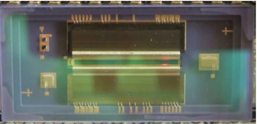
The PIC used during the test-bed assessment is here defined. The pho-tonic integrated circuit is placed and bounded on the tile with flip chip bound-ing technique, as shown in Figure 3.2. The electrical connections between the PIC and the PCB connectors have been already tested [24]. The circuit is a 8 × 8 optical switch (Nwg = 16) and satisfies all the requirements at
3.1 Photonic integrated switch 9
Figure 3.2. Photonic integrated switch 8 × 8 used during the test. Photonic integrated switch control
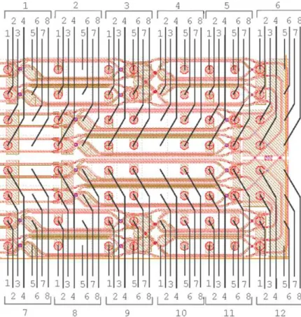
The switch function is provided, in an optical integrated circuit, by a matrix of SOAs [26]: they must be univocally identified in order to control the circuit.
A SOA is classified by its index and current value. As shown in Figure 3.3, there are 96 pads, divided in 12 groups with 8 tracks each one. The index is specified by matrix notation: indexgroup.indextrack. There are, at least, 2
pads per SOA while others are not connected, for instance: pad 1.1 and 1.2 are connected to the same metallization and 1.7 is not connected.
Current controller
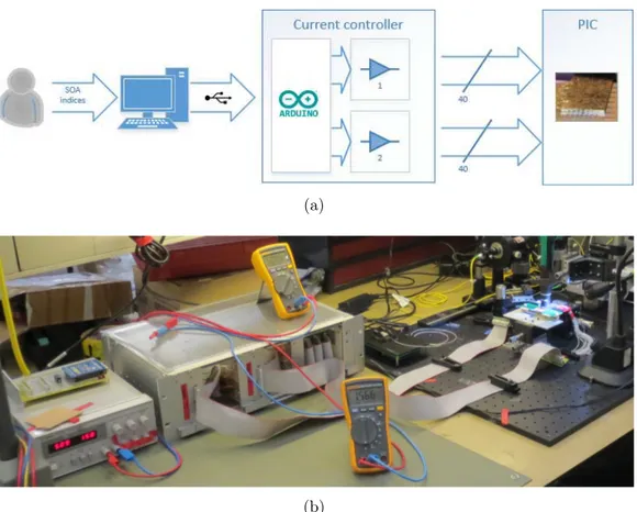
The PIC needs an interface in order to be controlled. A specific circuit (henceforth defined as current controller) and software were designed [27]. As shown in Figure 3.4, the operator inputs the SOA indices and their cur-rents by the software, the information are sent, through USB, toward the Arduino and this enables the output pins by means of 2 current drivers, each one can control up to 32 SOAs.
The software is provided with source code and the programming language is C++.
The setup is performed using a laboratory power supply: firstly a rack power supply was used, due to high current absorptions (about 6A in idle
3.1 Photonic integrated switch 11
(a)
(b)
Figure 3.4. The current controller; block diagram (a), setup, from left to right (b), the power supply, current controller (metallic rack box at the centre), the ammeter and voltmeter, the ribbon cables (one for each driver) and the PIC on optical board.
mode) and overheating, a laboratory power supply is used instead, therefore the problems are solved.
Current absorption spikes and voltage are monitored at board supply line through ammeter and voltmeter.
The connection between the drivers and PIC requires PCB plug adapters: electrical tests are performed to check the electrical continuity and the pin mapping.
3.2
Microlens array
3.2.1
Divergent multiple beams
The photonic integrated switch is a multiple port divergent source. This implies 2 problems: power distribution decreases with distance due to di-vergence (the path-loss is neglected) and a mutual interference is present between the beams.
Firstly, the simplest case is taken in account: only 1 PIC waveguide is enabled and in front of it the observer is positioned.
The received power decreases with the distance [28], while in transmission it is limited, therefore it is necessary to decrease the gap in order to increase the signal strength. If the observer is an optical receiver (photodiode or camera), this means decrease the placement tolerance and enlarge the positioning time, key features of this project.
Now a second case is considered: 2 more PIC waveguides are turned on, ray tracing is used to represent the beams and rectangular aperture diffrac-tion [28] is assumed to be negligible. As shown in Figure 3.5, the beams start to interfere at the distance Dif(henceforward called beam crosstalk). It can
be demonstrated by trigonometry as Dif depends on the distance between
the enabled waveguides, in the worst case they are adjacent, consequently Dif = 466.5µm.
The crosstalk can be reduced, even neglected, decreasing the distance be-tween the PIC and the receiver and this introduces the same problems of the
3.2 Microlens array 13
previous case.
It is clear the trade-off between received power, crosstalk and positioning tolerance: a solution could come from collimation.
A collimated beam is defined as a beam which has all the rays parallel one to the other [29]. Regarding the previous 2 cases, as shown in Figure 3.6, the great advantages are: the collimated beams can travel for longer distances than the divergent ones and crosstalk does not depend on the distance be-tween lens and receiver, therefore this can be placed more distant from the PIC, with relaxed precision. This solution also increases the flexibility of the test-bed: more devices could be placed between the photonic integrated circuit and the receiver to perform different tests.
3.2.2
Linear lens array
An array of lenses (hereafter called microlens array, MLA) is preferred to overcome the divergent beam trade-off.
The array features are: each lens can achieve the collimation only if it has the same axis of waveguide, all of them must be collimated at the same time, the reflection loss must be minimized and the device must be placed with relaxed tolerance. The lens array following with the constraints:
Figure 3.5. Mutual interference between 2 waveguides which emit at the same time. The 3 beams are displayed as triangles on the horizontal plane.
• lens pitches equal to Lwg;
• array of at least 32 lenses; • circular lenses;
• AR coating to minimize the reflection loss;
• good trade-off between focal distance and alignment tolerance.
The first parameters taken in account are the lens pitches, the number of lenses and their geometry. Besides, the Fresnel number (FN) is considered: higher values are preferred than the smaller ones, to decrease the diffraction effect on flat-top profile of lenses [30].
A Matlab script is written to compare the selected models, it takes as in-put: model code, radius of curvature (ROC), refractive index and NA. As shown in Figure 3.7, it displays and saves in a file: model, crosstalk condition fulfilment, focal distance, number of lenses and FN.
Figure 3.6. Top view of lens array collimation: the red rays are the inter-ferences, the black ones are the useful signals and Df denotes the lens focal
3.2 Microlens array 15
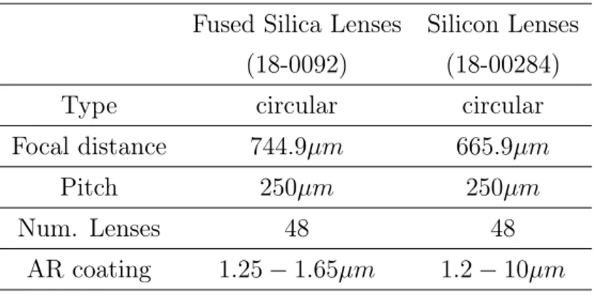
Table 3.1. The MLA model at the final selection. Fused Silica Lenses Silicon Lenses
(18-0092) (18-00284)
Type circular circular
Focal distance 744.9µm 665.9µm
Pitch 250µm 250µm
Num. Lenses 48 48
AR coating 1.25− 1.65µm 1.2− 10µm
The final choice is, as shown in Table 3.1, between two models with shortest focal distance. The best option is the microlens array, Silicon Lenses, model 18-00284, whose mechanical layout is shown in Figure 3.8.
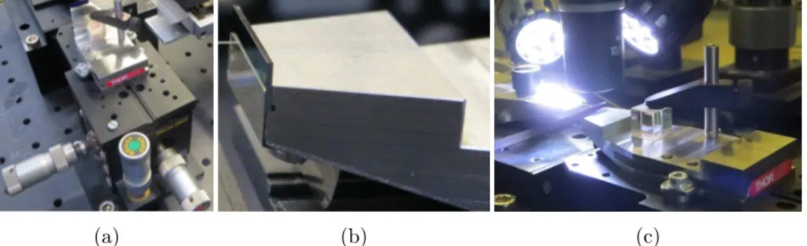
The small positioning distance and the size of the microlens array require a customized holder. As shown in Figure 3.9(a), the compatibility with other optical board holders and components and the high precision manufacturing led to a customized version of HFV002 - Tapered V-Groove Fiber Holder for Multi-Axis Stages [31] by Thorlabs, customized by Equipment & Prototype Center, TNO lab. located in Eindhoven, Figure 3.9(b).
As shown in Figure 3.9(c), web-cam microscope is used to have a visual feed-back during the MLA movement and avoid collision between the components.
Figure 3.8. Microlens array mechanical layout, vertical view, all the dimen-sions are in mm. The MLA thickness is 0.5mm.
(a) (b) (c)
Figure 3.9. The microlens array: full view of the holder and positioner (a), a detail of MLA and its holder (b) and the 3-axis stage used and web-cam microscope (c).
3.2 Microlens array 17
Tests
The microlens array is tested: the alignment procedure and the collimated beam are verified.
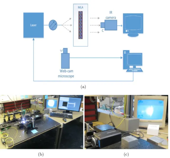
As shown in Figure 3.10(a) and Figure 3.10(b) the test-bed uses a laser [32] and an optical fiber as transmitter, the IR camera [33], displayed in Figure 3.10(c), as receiver; a red dot laser is also used during the alignment. The collimation is performed in 3 steps: firstly the microscope is used to align the optical fiber at focus distance with precision of few µm, secondly the MLA position is adjusted on vertical plane by the red dot laser (or IR card detector is used to shown the optical beam) and, finally, the fine collimation is performed by IR camera feedback, as shown in Figure 3.10(c).
Lens magnification problem. The magnification of the beam caused by mismatch of focus point is discovered and studied.
The lens magnification is a well known phenomenon: a lens of MLA is con-sidered, which in general is defined the vertical and horizontal planes, but is analysed on only one of these two planes (the analysis is the same for the other one). As shown in Figure 3.11, the optical fiber beam can be repre-sented as a spot on plane, near the focal point, at distance d0. The IR camera
is on the lens focal axis, behind it at distance di.
Defined h0 the gap between the spot height and the focal point:
• if h0 = 0 the spot is in focus point, the beam is collimated, and its
image is at infinity;
• otherwise magnification occurs: the image is at finite and shifted from the focal axis. The distance hibetween the receiver and the image spot
depends on di by the transverse magnification MT ≡ −dd0i = hh0i [34],
therefore, the beam is in a different position from the expected one. The magnification is more important when the receiver is far away from the lens and when it has a small width (for instance, the IR camera di ' 190mm).
(a)
(b) (c)
Figure 3.10. The test-bed scheme (a) and setup (b), from left to right: the 1550nmand red dot lasers, the optical fiber, MLA and IR camera, the screen used to display the camera output and the computer to control the laser and microscope display. A detail of the receiver (c): the white spot on screen is the almost collimated MLA beam.
3.3 Optical receiver 19
Figure 3.11. Lens magnification in a coordinated plane.
The problem occurs both on vertical and horizontal plane, producing a spot out of camera sensor. This is the reason to use the red dot laser: it allows to perform a first raw and fast alignment, and, secondly, the fine adjustment is performed by IR camera.
Performances
The alignment and the collimation are performed in a few hours. A great advantage is given by red dot laser which allows the placement without IR card detector and through immediate visual feedback. The microscope is used only for the first alignment and for safety reasons, avoiding optical fiber crack on MLA surface. The focal distance allows the fine adjustment without optical feedback through microscope and reduces the alignment time.
3.3
Optical receiver
The beam acquisition is one of the most important features of the test-bed and is performed by an optical receiver. It follows with characterization:
• peak wavelength at 1600nm;
• incoming beams collection at the same time;
Figure 3.12. Photodiode array PDA-640 SFF InGaAs Photodetector Sensor by Princeton Lightwave Inc. in place on PCB slot.
• calculation of maximum power positions (peaks) and the total emitted power.
The receivers based on optical fibers are discarded immediately: the precision required in positioning increases placement time and placement precision. The optical power linear distribution along the PIC waveguide alignment direction is the useful one, therefore a linear array of photodetector is chosen. As a further advantage, if the array is selected with a sufficient sensor area, the alignments will require higher tolerance.
3.3.1
Photodiode array
The previous requirements lead to choose the linear array 640 pixels PDA-640 SFF InGaAs Photodetector Sensor (PDA) by Princeton Lightwave Inc., as shown in Figure 3.12, following with characterization.
Maximum power. The PDA maximum received power (denoted as Prx,max)
is calculated and is equal to 11.67dBmW, as verified at page 99.
3.3 Optical receiver 21
Figure 3.13. PDA pixel arrangement layout: all the dimensions are in mm. Photodiode arrangement. The PDA provides, as shown in Figure 3.13, a row of 640 active pixels, 8 dark pixels and 8 disconnected pixels on each side. The dark pixels record the power provided by dark current and the disconnected ones give unreliable values which must be deleted during data processing.
The pixel dimension are 20 × 500 µm × µm which is sufficient to acquire the collimated beam of diameter Lwg. The total array length is 12.8mm and is
adequate to acquire all the photonic integrated switch beams at the same time.
Inputs and outputs
The most important inputs and outputs are here described. The other data and timing specification are in datasheet at page 77. The signal func-tions are the following:
• clock, from 0.01 to 5MHz;
• Integrate, input signal which control the integration and readout; • Even Video 1 and Odd Video 1, pixel video reference levels outputs,
updated on falling and rising clock edge, respectively;
• Even Video 2 and Odd Video 2, pixel video level outputs, updated on falling and rising clock edge, respectively;
when the integrate signal is activated the photodiode array starts to acquire the optical signal, thereafter the data are output: each pixel is provided with readout circuit which provides the signals (in parallel), the PDA puts these values in serial on Even and Odd Video pins. The sampling time and pixel
Figure 3.14. PDA electrical scheme from the datasheet at page 77. rate depend on the clock frequency.
The relation between output voltage and optical power Prx(t) is calculated
by analysing the electrical scheme shown in Figure 3.14. The readout cir-cuit is an integrator operational amplifier followed by a sampler. The sam-pler input voltage (Vout) is defined in (3.2): the VRef, CIN T, Tint and ip(t)
are, respectively, the voltage reference, the capacitor used in the integrator, the integration duration and the photodiode current. This depends on R, Idark and Ing,opt, which denote respectively the responsivity, dark current and
negative-going current of pixel photo-detector.
ip(t) = R · Prx(t) + Idark+ Ing,opt (3.1) Vout = VRef − 1 CIN T Z Tint 0 ip(t)dt (3.2)
3.3.2
Interface board
The photodiode array must be controlled and interfaced toward the com-puter. Therefore, the following functions must be provided:
3.3 Optical receiver 23
• 6 input signals processing and voltage supply; • analogue-to-digital conversion of 5 output signals;
• computer interface handling and software library for the test-bed soft-ware.
The 640 Pixel Linear PD Array Demo Board (henceforward called PDA-board) by Princeton Lightwave Inc. is chosen as computer interface.
The data loggers by Pico Technology were also considered: the limited output voltage range, the dearth of software library which directly supports the PDA and the estimated time necessary to design a reliable receiver led to select the Princeton Lightwave Inc. solution.
PDA-board
The PDA-board provides all the requirements previously defined: it con-verts the input parameters into the proper PDA signals and performs the analogue-to-digital output conversions, providing the number of samples for each pixel. As shown in Figure 3.15, the board requires the power source, computer link (via USB interface) and the PDA connection. All the other signals are generated inside.
From the software support perspective, the board is supplied with a graphical user interface (GUI) software and dynamic-link library (DLL) func-tion set. The provided software, whose graphical user interface is shown in Figure 3.16, is able to set all the PDA parameters. Moreover, it provides the test function which checks the link between the board and computer and the possibility to save the output on a tab delimited text file.
Both the graphic and the output file provide the power distribution along the sensor line: the output is a 672 element vector. The ith value of this vector is
the optical power received by the ithpixel. The power values are expressed in
samples, a quantity which represents the number of samples used during the analogue-to-digital conversion performed by PDA-board. The relation
be-Figure 3.15. Interface board: top view of PDA-board, from left to right, the ribbon cable used to connect the photodiode array, the power supply and the USB cable.
tween power in samples and Watt units is studied and the linear dependence between these quantities is demonstrated in section II.
3.3.3
Tests
Test-bed setup
The photodiode array performance is tested to establish the simulation and environmental parameters affect the measurements. The Tint and the
number of measurements (NLines) are studied as well as the high and low
frequency electromagnetic (EM) interferences and the minimum distance be-tween beams recognized through the photodiode array. Finally, an unex-pected problem in PDA-board output is studied and solved.
As shown in Figure 3.17, the test-bed configuration is similar to the one described at page 17: the optical source is the same, collimated by MLA, the web-cam microscope and the beamsplitter are still positioned. As displayed in Figure 3.17(a), the IR camera is moved to place the PDA, the beamsplitter [35] allows to divide the beam, as a result the IR camera is moved in front
3.3 Optical receiver 25
(a)
(b) (c)
Figure 3.17. Test-bed used during PDA trials: diagram scheme (a) and setup (b). The PDA is placed in the metal box on the vertical positioner, in the centre of the image, and is connected through a ribbon cable to the PDA-board. The red dot positioner is reported in (c). The bottom post mount fixes the altitude, the upper one rotates in order to point, firstly, the MLA and, finally, the PDA performs the alignment.
of the second output in order have an extra optical receiver.
The alignment procedure is divided in 2 steps: horizontal and vertical positioning. The first stage is simplified by the fact that the photodiode array width is bigger than the beam diameter and is performed by rough visual alignment. The similar dimension of PDA pixel pitch and optical
3.3 Optical receiver 27
Figure 3.18. Saturation effect versus Tint.
beam wavefront increases the vertical alignment time. The solution is to use a red dot laser pointer, as shown in Figure 3.17(c). In this way, the time required is reduced to few minutes.
Measurement time versus saturation
The effect of Tint variation on the photodiode array output is measured.
As shown in Figure 3.18 and as already defined by the mathematical model of (3.2), the received power rises for increasing Tint, up to the level
corre-sponding at ' 50000 samples (Countmax). Values of optical power greater
than Countmax are analogue-to-digital converted equal to Countmax. This
phenomenon is denoted as PDA saturation.
The Tint can be set by different parameters, such as the clock divisor and
the integrate clock number, and the power distribution behaviour does not change from the response reported in Figure 3.18. Same data and conclusion are provided by the tests performed changing the CIN T.
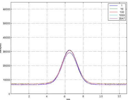
Number of measurements versus data reliability
The variation of the optical received power was discovered during the tests, for the same transmitted signal and test-bed conditions. As shown in Figure 3.19, the number of measurements NLines influences the reliability
of the output data. Indeed, the relative error of the maximum between NLines = 1 and NLines = 2047is 6.574%, while it decreases to 0.29% between
NLines = 1000 and NLines = 2047. As consequence NLines determines the
number of reliable digits in all the output data, and the possibility to reveal the minimum power change is not caused by the random variation of the received optical power.
Figure 3.19. Power distribution variation versus NLines.
Electromagnetic interference
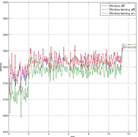
The possible interference by electromagnetic fields at low and high fre-quencies was studied as well.
The electrical grid interference was studied to know if the other test-bed devices affect the photodiode outputs: the CRT monitor and red dot laser
3.3 Optical receiver 29
current spikes during the enabling are used as burst EM interference sources. As shown in Figure 3.20, the device interferences do not affect the PDA data reliability, since the three cases provide negligible variation of the average power.
Figure 3.20. Comparison between optical power distribution with and with-out electromagnetic interference caused by electric grid. The mean values for the blue, green and red curves are, respectively, 5221, 5193 and 5223 sample. The high frequency interference are also tested, in particular, environ-mental light (especially the microscope light) produces a flat interference pattern which becomes more important with the increase of Tint.
However, this interference does not affect the output values, inasmuch it can be recognized and erased by software algorithm during the data processing. The interference adds power to the optical beams received, reducing the num-ber of samples available for the useful signal or, as well as, saturating the
PDA.
As shown in Figure 3.21, the interference is sensibly reduced using a dark-room for PDA. Indeed, the environmental light interference, in this condition, is negligible, inasmuch the darkroom provides as environmental interference as the ideal condition, which is no light in the laboratory.
Spatial resolution
The photodiode array length is sufficient, as written at page 21, to acquire all the photonic integrated switch beams. This simplifies the measurements but, more important, allows to recognize the position of each beam and distinguish it from the others. This feature makes possible to perform new tests on the PIC: optical crosstalk, measure erroneous waveguide routing and SOA mapping.
The position identification depends on the spatial resolution of the PDA. This quality can be defined as the minimum distance between the maximum
Figure 3.21. Environmental light (Tint= 1.5ms) interference: the dark-room
3.3 Optical receiver 31
Figure 3.22. Spatial resolution test-bed changes: the optical fiber connected to Laser 2 is collimated and can shift along the yellow arrow direction.
Figure 3.23. The spatial resolution results: the second beam is saturated by purpose in order to display more clearly the signal collimated by the MLA. The displayed distances are the relative gaps.
of 2 beams. The peak and its position are necessary to calculate the mean value and the variance of the theoretical gaussian curve.
As shown in Figure 3.22, the trial is performed adding a second collimated optical fiber in the test-bed. The results obtained are shown in Figure 3.23, where the microlens array collimated signal is the lower peak in each curve and where the second beam is saturated in order to increase the measurement precision. Therefore the minimum recognizable distance is 980µm.
Offset equalization
The PDA-board data ripple problem is here defined and solved.
As shown in Figure 3.24, the trials performed with PDA-board provide a power distribution with an unexpected ripple and the same issue is verified also with the provided DLL function set.
The output curve generated by the PDA-board software allows a more de-tailed analysis. In this way, it is discovered that the ripple is present between the odd and the even values: the output elements with even indices do not have ripple, since the datum variations are consistent with the expected beam, and the same is verified with reference to the odd index elements. Consequently, the ripple is limited between 2 envelopes defined by the even and the odd vectors.
The problem cause is then analysed. At first, the optical source is in-vestigated as a possible cause of the ripple but it is still present when the photodiode array is shut and the photocurrent is constituted by the noise of the receiver. Moreover the ripple is present also in the dark pixel val-ues. Consequently, the cause is not the external source. Secondly, a possible photodiode array malfunctioning is supposed, but the ripple is also present in test pattern generated by the PDA-board, without regard for the photodiode array. It is then concluded that the ripple must be related to the board. The photodiode array data are supplied through Odd Video ad Even Video outputs (see at page 21) and a mistaken PDA-board offset compensation calibration of these pins generates the ripple [36]. This ripple cannot be
3.3 Optical receiver 33
Figure 3.24. Screen shoot of the PDA-board software in which the power distribution ripple is shown. On the abscissae and ordinates are displayed, respectively, the pixel index and the power in samples.
tuned through a circuital calibration. Anyway, the data are still reliable [37], therefore the offset equalization is performed by software during the data processing.
The equalization algorithm is based on odd and even indices separation, the 672 elements vector provided by the PDA-board (v) is split in even and oddvectors as shown in (3.4) and (4.1), respectively.
eveni = i = 2, . . . , 672 vi if i is even or i=1, vi−1+vi+1 2 otherwise. (3.3) oddi = i = 1, . . . , 671 vi if i is odd or i=672, vi−1+vi+1 2 otherwise. (3.4) The even and odd vectors describe 2 different power distribution en-velopes. Therefore the photodiode array parameters influence on them are studied and the most reliable vector is selected. As shown in Figure 3.25, even is chosen due to the smaller offset introduced, which means a reduced probability of PDA saturation and increased reliability against the NLines
(a) (b)
Figure 3.25. Power distribution versus NLines: even (a) and odd (b), the
offset in smaller in the first case than the second, as well as the relative error decreases faster with NLines for even than odd.
3.4
Software
The project goals require to write the software necessary to control the test-bed: 3 programs are written to this purpose.
The communication between PDA-board and computer is achieved by the supplied DLL function set. The connection toward the current controller is performed by the function set developed in the same project [27].
The software is development using the following tools: • Windows XP operating system, service pack 3; • Standard C++ programming language;
• NetBeans IDE 7.3.1 (Build 201306052037); • MinGW C++ 4.6.2 compiler;
3.4 Software 35
3.4.1
Data displayer
software
The first software is Data displayer: as shown in Figure 3.26, it is a graphical user interface program for the real-time display of recorded power distribution curve, total power, maximum and peak position.
The Data displayer main purpose is to enable the operator to use the photo-diode array as a linear IR camera, providing the immediate PDA data with-out performing multiple acquisition, the Data displayer is designed to sim-plify the alignment step through the photodiode array feedback, leaving the operator focused on the device alignment procedures.
The software is written by the programming language Standard C++, moreover the Qt and QCustomPlot [38] – [40] graphical user interface libraries are used.
As shown in Figure 3.26, the graphical user interface has 3 buttons and 4 displays: the peak position and peak value windows, the total power and the power distribution displays. All the power values are declared in samples and the power distribution is shown in pixels versus samples.
The button actions call the function declared in Listing 3.1. The graphical interface provides then the buttons, start, stop and capture with the following functions:
• when for the first time start is clicked, the function start () is called and performs the photodiode array initialization. Otherwise, if start is clicked meanwhile the measurement is stopped, it will start again the acquisition.
• When the stop button is clicked, the function stop() performs the dis-connection.
• When capture button is clicked the displayed distribution is saved in Value.csv file by the function capture().
The procedure result is shown in the display below the buttons through the messages: ‘connected’ (green background) or ‘error’ or ‘disconnected’ (red
Listing 3.1. Data displayer class declaration of public functions. class PDA−GUI : public QDialog {
Q_OBJECT public:
PDA640SFFBoard_H();
virtual ~PDA640SFFBoard_H(); public slots:
// connect the board void start ();
// disconnect the board void stop ();
// display pattern void updateCurve();
// save in .csv file the pattern void capture();
3.4 Software 37
Table 3.2. Data displayer input, output files: name and description.
File Type
SimParameters1.csv Input: define low sensitive PDA parameter SimParameters2.csv Input: high sensitive PDA parameter
Value.csv Output (optional): generated by capture()
LogFile.txt Output: logfile
background). Furthermore, a logfile is written to report all the errors oc-curred.
The typical Data displayer usage is: start the program, clicking start button, and in this way the graph displays the different patterns. When a distribution needs to be saved: stop button is clicked, the pattern remains in the graph, and with capture button it is saved, the measurements restarts, newly, click-ing the start button.
The real-time visualization is obtained by a timer: when the count is finished the curve is updated and displayed by the function updateCurve() and then the timer starts again to count.
Dark values cancellation. The dark current offset by dark pixels is deleted. After the acquisition, the program discards the values provided by the dis-connected pixels. To this purpose it calculates the mean value of dark pixel elements in order to find the dark offset, then it subtracts the result from the active pixel vector. Finally, the power values provided do not depend on the dark current.
Parameter autoset. Some tests are performed changing the laser power in a wide range, the PDA acquisition parameters must be set frequently in order to better display the data. An automatic setting of the simulation parameters is needed (autoset): this feature is programmed in order to recognize when the pattern is badly displayed and, in case, to change automatically the PDA
Figure 3.26. Data displayer: the graphical user interface.
parameters between 2 different configurations avoiding saturation or low peak values.
Inputs and outputs. All the input and output procedures are performed by the file shown in Table 3.2, in which SimParameters1.csv and SimParam-eters2.csv are the files used for the autoset feature. No output is generated unless the function capture() is invoked. The logfile is generated to record all the software activities and failures.
3.4.2
Test controller
software
The second, and main, test-bed software is the Test controller: as shown in Figure 3.27, it is a command line interface developed in Standard C++. The main purpose of the Test controller is to supply a software able to man-age all the test-bed during the trials, from the photonic integrated switch transmission to the photodiode array acquisition. It is designed to perform automatically all the operations of a typical photonic integrated switch
op-3.4 Software 39
tical test (PIC enabling, PDA acquisition and data saving) without the op-erator control. Moreover, a semi-automatic mode is implemented in order to control the PIC during the alignment procedures.
The sequence of SOAs, their currents, as well as all the PDA parameters are specified by Comma Separated Value (.csv) files listed in Table 3.3. The out-put values and the status flags are not shown on screen but saved in outout-put and log files.
Table 3.3. Test controller input and output files and folder: name and de-scription.
File and folder Type
SimParameters1.csv Input: define low sensitive PDA parameter SimParameters2.csv Input: high sensitive PDA parameter
PICAlignment.csv Input: SOA sequence
PICMeasureSequence.csv Input: SOA sequence
OutputParameters.csv Output: maximum and power
patterns/ Output: recorded patterns directory
LogFile.txt Output: logfile
The program provides two operating modes: alignment and measure-ments.
• The alignment mode is designed for the photonic integrated switch posi-tioning steps. The software loads from PICAlignment.csv the photonic integrated switch SOA current and indices: neither the photodiode ar-ray, nor the output recording are controlled. They are instead managed by the Data displayer.
• The measurements mode manages both the current controller and the PDA-board. In particular, it initializes the devices, loads the set of SOA from PICMeasureSequence.csv and enables it. Subsequently, the
3.4 Software 41
Listing 3.2. Test controller PIC class declaration of public functions. class Controller{ public: Controller (); ~Controller(); // initialization function string Init ();
void getSimData(int & NumCopiedEntry, string & InputFile); // set read input
int SetOutput(int & SimIndexEntry, bool & ReturnedValue, bool & CalibrationMode); };
program performs the data acquisition and saves the read values in OutputParameters.csv and in the patterns folder. Thereafter, the next set of SOA is loaded and the same procedure is repeated. No operator control is required.
The modes are based on 2 classes: Controller and PDA640SFFBoard_H. Controller manages the photonic integrated switch and its public functions are shown in Listing 3.2.
When the Test controller starts, three functions are called, which are listed below.
1. The function Init () is called to initialize the current controller outputs, therefore the operator chooses a mode: alignment or measurements. 2. The function getSimData(int & NumCopiedEntry,string &InputFile)
speci-Listing 3.3. Test controller PDA class declaration of public functions. class PDA640SFFBoard_H {
public:
PDA640SFFBoard_H();
virtual ~PDA640SFFBoard_H(); //connect the board
void start ();
// disconnect the board void stop();
// check temperature void checkStatus(); // save data
void capture(bool & CalibrationMode); };
fies the name of the file to load (PICAlignment.csv or PICMeasureSe-quence.csv) and returns the number of imported rows by NumCopiedEntry, the data are saved in a private array.
3. The function through which the software sends the SOA information to the current controller, which is the function SetOutput(int & SimIndexEntry, bool & ReturnedValue, bool & CalibrationMode). The sequence which has to be set is specified by the parameter SimIndexEntry. All the spec-ified SOAs are enabled and the result is returned by ReturnedValue, and will be true if the procedure returns correctly, false otherwise. Besides, the function returns CalibrationMode=true if the first SOA index has current equal to zero. The meaning of this parameter is explained below where the PDA640SFFBoard_H is described.
As shown in Listing 3.3. The second class PDA640SFFBoard_H controls the photodiode array. When measurement mode is activated the Test controller
3.4 Software 43
in addition manages the photodiode array through PDA640SFFBoard_H, following with the algorithm:
1. the constructor PDA640SFFBoard_H() initializes the object and loads the default measurement parameters by SimParameters1.csv.
2. The connection and disconnection are performed, respectively by the functions start () and stop(). In case of failure the functions write in LogFile.txt and exit the program.
3. The function SetOutput() is called.
4. A delay of 10s is waited in order to be sure that the photonic integrated switch outputs are stable.
5. The function checkStatus() is called to check the temperature of the PDA-board. If the temperature is greater than 65◦[C] the board will
be disconnected, the logfile is updated and the program is terminated. 6. The function capture(bool &CalibrationMode) saves the acquired dis-tribution. CalibrationMode is a flag which communicates if the next power distribution is a interference pattern. This is used to perform the interference cancellation. Usually the special entry is specified in the first row, but it can be written more times in the file in order to update it. In this case the software recognizes each time the entry and updates the interference array. This procedure works as follow:
• if CalibrationMode=true, the function sends the measurement parameters to the board, starts the acquisition, receives the tribution from PDA, performs the autoset and memorizes the dis-tribution in a particular array as interference pattern. The entire array is saved in the file <measurement time>.csv in the patterns folder;
• if CalibrationMode=false, the function performs the same opera-tion of the previous point and from the received distribuopera-tion the interference array is subtracted. Besides the maximum, its posi-tion and the total power are calculated;
The function saves other values in OutputParameters.csv: these are SOA index, current, peak position and value, total power, measurement PDA file used and time.
The Test controller flowchart is shown in Figure 3.28. The PDA class also performs the dark power cancellation in the same way provided by Data displayer software as explained at page 37.
3.4.3
Data analysis
The data supplied through the photodiode array must be processed in order to extract the searched information. The data elaboration is then performed by a Matlab software. The script developed allows to display the current versus the power, the full width at half maximum and the current-space power distribution.
The script performs the following steps:
1. the program copies patterns folder, OutputParameters.csv, LogFile.txt, SimParameters1.csv and SimParameters2.csv from Test controller to the specified target folder.
2. The program reads from OutputParameters.csv, currents, total and maximum power and memorizes these values in 3 different arrays. 3. The software imports all the power distribution in comma separated
variablefiles from the patterns folder and saves them in the P owerP atterns (640 × NumberOfMeasurements matrix).
4. The current versus power curve is then obtained displaying the current and total power arrays with the plot() function. The figure obtained is saved in .fig, .eps and .jpeg formats in the target folder.
3.4 Software 45
Figure 3.28. Algorithm of a typical use of Data displayer and Test controller in alignment and measurement procedures.
5. The full width at half maximum versus SOA current is then calculated. The theoretical half maximum power is calculated for each SOA cur-rent, then the closest real values are searched in the array and their positions are returned. The indices are 2: one on the left and one on the right of the peak. The full width is calculated making the difference of these two values. The full width versus current arrays are displayed and saved in .fig, .eps and .jpeg formats in the target folder.
6. The power distribution is displayed in function of the pixels and the SOA currents. These two are shown in abscissae and ordinates axes, re-spectively, and the power values are represented through a color scale. The color-bar graph, which is a 2 dimensional graph, exploiting the script normalizes the P owerP atterns 50000 samples value to 255 (max-imum of RGB color scale), in order to have the same scale for all the graphs, the behaviour of the curves is displayed with the function im-age() and saved in the .fig, .eps and .jpeg formats in the target folder. 7. The script deletes all the read data from the software folder making it
Chapter 4
Test-bed assessment
In this chapter the test-bed evaluation, performed by photonic integrated switch trials, is reported. The prototype used is described in subsection 3.1.2. The tests performed are two: waveguide characterization and optical conti-nuity.
The methodology used is a bottom up approach. Initially, the current con-troller outputs are verified, the photonic integrated switch is positioned and collimated in section 4.1. Then, the first, simple test is performed: one outer photonic integrated switch SOA at a time is enabled and studied in sec-tion 4.2. Finally, the second trial is performed, the complexity is increased inasmuch multiple inner SOAs are enabled in the same measurement and the continuity of a PIC optical path is analysed in section 4.3.
4.1
Preliminary operations
The photonic integrated switch optical tests require that all the test-bed devices are verified before the trials, in order not to affect their reliability. The only component to be checked is the PIC, because all the other devices are already tested in chapter 3, therefore it is assured that they work cor-rectly. The photonic integrated switch check is divided in two stages: current controller output and PIC collimation.
The photonic integrated switch SOAs are identified by their indices and currents, as explained at page 9. Therefore it is necessary to match the values provided by Text controller with the current controller pinout and currents, in order to be sure to enable the correct SOAs.
The pinout test is performed verifying that the SOA indices input in Test controller match the PIC connector tracks of the trial sample: this allows to emulate all the test-bed from the program up to the PIC ceramic tile. The check is accomplished measuring the track voltages: if they are supplied to the given pads the test is passed, otherwise the pinout is wrong and is changed by software.
The current output is verified for each SOA with the following procedure. The test is based on providing a current value by Test controller and measuring the output current of the power supply when a diode connected in series to 5Ω resistive load is used as SOA model. The measurement algorithm is composed by the following steps:
1. the PIC output are disabled → the current measured is the idle current controller value;
2. the SOA is enabled by 0mA → the measured current is the reference value;
3. the SOA current is increased → the power supply current is measured; 4. the real SOA current is calculated as difference between the measured
and reference values.
As shown in Table 4.1 and Table 4.2, if the load has a finite resistance the measured value will be valid, otherwise it is an open circuit and the current is not matched, theoretically it tends to zero. This method gives a great ad-vantage, since it allows to check the photonic integrated switch SOA status before performing the optical test and in a shorter time: if the measured current for a SOA is not matched, this will be broken.
4.1 Preliminary operations 49
The photonic integrated switch collimation is the second, and last, stage. The chip is positioned on a two axis positioner ables to move in vertical di-rection and toward the microlens array. Neither the red dot laser, nor the IR detector card can be used, due to photonic integrated switch characteristics: a new collimation procedure is designed. As shown in Figure 4.1 and Fig-ure 4.2, the alignment is performed in 3 steps: firstly, a coarse placement is performed by IR viewer [41], secondly the IR camera with diaphragm is used and, finally, the photodiode array performs the fine alignment. As displayed in Figure 4.1(a), the IR viewer is placed in front of microlens array. When the PIC spot is displayed (Figure 4.1(b)) the diaphragm is narrowed and the PIC moved to see it again, finally, the beam spot is limited to a few squared mm. As shown in Figure 4.2(a), in the second stage the IR viewer is moved backward on the positioner rail and the camera is mounted in front of it, the two sensor centres are aligned one with respect to the other and the PIC is collimated with greater precision, therefore the third step is performed. As displayed in Figure 4.2(b), in this stage the IR camera is moved backward on the rail and the photodiode array is placed and aligned through the feedback of Data displayer. As a result the PIC beam is collimated.
During the entire procedure and the optical tests the following PIC safety rules and advices are strictly followed:
1. typical current values, lower than 30mA for alignment and lower than 80mA for measurements.
2. Limit of the SOA enable time, it depends on the current, according to the following relationship.
time = (
30M in. if SOA current < 35mA,
15M in. if SOA current ∈ [35, 70]mA. (4.1) 3. Turn-off period between each session 5Min..
4. In front of a drastic power decrease (which is due to overheating) the input current must be immediately switched off.
(a) (b)
Figure 4.1. The first step of the PIC collimation procedure: the IR viewer test-bed setup(a). The IR view of the PIC beam by IR viewer(b): the green dot is the beam through the MLA, the microscope lens can be recognized over the MLA.
(a) (b)
Figure 4.2. The second and third step of the PIC collimation procedure: the IR camera is used for the fine adjustment (a) and, in the next step, the photodiode array is placed (b).
5. During the alignment procedure, only one pad at a time must be en-abled for the same SOA.
6. The red dot laser must not be pointed toward the photonic integrated switch ports.
4.2 Waveguide characterization 51
Table 4.1. The SOA 1.1 current check: the variations are valid. The idle current is 1.548[mA].
Input [mA] Current at power supply [mA] pin output [mA]
0 1.564 0
10 1.575 11
30 1.594 30
45 1.608 44
Table 4.2. The SOA 1.3 current check: the variations are not valid and the connection is broken. The idle current is 1.545[mA].
Input [mA] Current at power supply [mA] pin output [mA]
0 1.5556 0
10 1.557 -7
30 1.559 -5
45 1.561 -3
7. The PCB PIC connector must not be crushed into the microlens array holder.
Finally, the test-bed setup is ready. As shown in Figure 4.3, the test con-troller manages the PIC input as well as the photodiode array acquisition, the output files are saved in OutputParameters.csv file and patterns directory, the Matlab processes the data and the curves and data are shown.
4.2
Waveguide characterization
The photonic integrated switch optical tests are performed acquiring the beam transmitted. Therefore it is necessary verify if, and how, its waveguides emit the signal. This can be achieved enabling the first SOA of each PIC port: as shown in Figure 3.3, these are the SOAs 1.1, 1.3, 7.3 and 7.1 (from now on they are called edge SOAs).
Figure 4.3. Schematic diagram of test-bed used during the photonic inte-grated switch trials.
4.2 Waveguide characterization 53
The port capability to transmit is proved verifying the waveguide position, and finding the relation between current and optical power as well as measur-ing the beam width. The first trial recognizes the beam positions and checks the correctness of the photonic integrated switch inner routing. The current versus power test inspects the SOA efficiency to convert the electrical signal into optical power. Finally, the beam width analysis verifies the signal power spreading measuring its full width at half maximum (FWHM) at different currents.
4.2.1
Waveguide positions
The test is designed to verify the PIC beam positions: it is performed, firstly, enabling the edge SOA, secondly, the photodiode array acquires the power distribution and, finally, the peak position is controlled.
As shown in Figure 4.4, the beam spatial disposition is, from left to right: 1.1, 1.3, 7.3 and 7.1. The port order is reversed, if it is compared with the PIC layout, due to the photodiode array placement. However, this does not influence the measurements.
Microlens array tilt. On the vertical and horizontal planes a relative tilt is found between the microlens array and the PIC waveguide lines. Conse-quently, they are not parallel and the MLA must be collimated in vertical direction: each time a different edge SOA is enabled.
The device visual inspections through microscope allow to calculate the tilt angle on horizontal plane which results equal to 2.245°. The vertical tilt angle is estimated with a different procedure: to this purpose is used the microlens array vertical movement necessary to collimate each waveguide is used. As shown in Table 4.3, the vertical position adjustments require some tens of µm movements and are not constant between the waveguides.
The relative tilt is not observed during the optical fiber preliminary tests since more than one optical source is necessary to experience the problem.
(a) (b)
(c) (d)
Figure 4.4. SOA power distributions at 30mA: 1.1 (a), 1.3 (b), 7.3 (c), and 7.1 (d). Maximum position, in mm: 6.24, 6.8, 8.16, 9.76, respectively.
4.2 Waveguide characterization 55
Table 4.3. The SOA indices versus the vertical position variation: for each SOA position change is shown the estimated correction on vertical MLA position.
SOA index change Vertical adjustment [µm]
7.1 → 7.3 62.5
7.3 → 1.4 25
1.4 → 1.1 50
1.1 → 7.1 37.5
4.2.2
Current versus power characteristic
The trial finds also the relation between SOA current and its optical power as well ass the beam width. The test is performed in two stages: firstly, the SOA is enabled with current going from 0 to 75(mA), with step of 1(mA), and the power is acquired. Then, the data are processed in order to provide the behaviour of the current versus the optical power and the full width at half maximum curves, as explained at page 44.
The color-bar graph gives, at the same time, the information about the current versus power distribution and the peak. It shows the maximum power changes with current, abscissae axis, and the spatial power distribution, or-dinates axis. As shown in Figure 4.5, the SOA 1.4 cannot work properly: this was discovered previously by the current checks at page 48, confirming the validity of current absorption as a valid connection verification method. Besides, the same SOA is not working correctly with the other connector, 1.3: the waveguide position trial shows different results but after few starts its performance decreased.
As shown in Figure 4.5, the SOA 1.1 and 7.1 have better performances than 7.3, due to the higher optical power reached for the same supplied current. The current versus power curve is illustrated in Figure 4.6: the 1.1 and 7.1 better performances are confirmed, furthermore the curve behaviour at low current values are shown.
The full width at half maximum graph is displayed in Figure 4.7: it re-mains almost constant for all the currents. The spikes at the lowest current values are caused by post-processing mismatch. At those currents the distri-butions are flat and the error caused by theoretical and real half maximum discrepancy are greater than for the other current values.
4.3
Optical continuity test
The photonic integrated switch function is to address the optic beam from the input toward the desired output port. The optical integrity is a fundamental requirement for the correct operation.
The photonic integrated switch optical paths are defined as the paths be-tween two edge SOAs. An optical path in which the beam propagates from one side to the other of the way is defined as continuous.
The trial here performed verifies the test-bed capability to analyse the con-tinuity of an entire PIC optical path.
4.3.1
Optical path structure
As shown in Figure 4.8, the most simplified PIC optical path model is defined as a sequence of stages, each one composed by a SOA (active com-ponent) and passive devices (coupler, etc.).
The stage working point definition is introduced as the current for which the SOA amplified spontaneous emission (ASE) balances the stage loss. There-fore, each stage has 3 states:
1. continuous path and current lower than working point. The current supplied to the SOA is insufficient, therefore the emitted photons can-not balance the stage loss [42], and its link budget is negative (the stage output power is lower than the input value).
2. Continuous path and current greater or equal than working point. The SOA emission balances the loss and the power contribution of the stage
4.3 Optical continuity test 57
Figure 4.5. Time-spatial power distribution SOA 1.1 (a), 1.3 (b), 7.3 (c) and 7.1 (d), on abscissae and ordinates axes are shown the supplied current and the array line in pixel, respectively.
Figure 4.6. Edge SOAs current versus power.
Figure 4.7. Edge SOAs full width at half maximum (FWHM). is not negative.
3. Optical discontinuous stage, no matter which current is supplied, the stage loss is not balanced;
4.3 Optical continuity test 59
Figure 4.8. Schematic diagram of a photonic integrated switch optical path, the N stages and their model (SOA and passive components): the 1st SOA
is an edge SOA.
4.3.2
Working point survey
The suitable current to determine the working point must then be found. This requires two steps: finding the maximum SOA current and ranging it in order to discover the working point.
Firstly, the upper range bound is calculated for each stage. The edge SOA maximum current and their contact areas are known, therefore the current density is calculated which is equal to 9.66MA/m2. The surface of the stage
SOA is known, therefore the maximum current is computed and matched during the trials.
Denoting the ith SOA as SOA
i with i = 2, ..., N, its working point is found
studying the current versus power curve. As shown in Figure 4.9, an iterative algorithm is used:
1. the SOA1,..., SOAi−1 are enabled with their known working points;
2. the SOAi is enabled with the current in the calculated range;
3. the current versus power is computed and analysed, as shown Fig-ure 4.10;
the step 1 is performed in order to bring the beam to the photonic integrated switch port. The trial can be performed when the ith SOA beam travels
up to the photonic integrated switch port and reaches the photodiode array. Therefore, a continuous optical path must be provided between the port and
Figure 4.9. Working point survey flowchart: I-P test denotes the current versus power trial.
Table 4.4. SOA working points: switches with similar surface areas have comparable currents.
SOA 7.3 8.4 9.8 11.8 12.4 12.2 11.6 9.6 8.2 7.1
Current [mA] 30 60 255 40 255 28 20 40 60 30
the studied inner SOA, the step 1 provides the necessary way.
As shown in Figure 4.11, the tested photonic integrated switch optical path and the SOA indices are defined. Consequently, the working point survey results are found and shown in Table 4.4: the SOA 12.4 reaches the maximum supplied current (255mA), without a clear working point.
Besides, during the test, the current absorption check of page 48 is performed: no broken SOAs are found.
4.3 Optical continuity test 61
Figure 4.10. Power versus current curve of SOA 9.8, the loss is balanced for I ' 200mA, as a result the working point is select equal to 255mA.
![Figure 1.1. Technological trends between the 2011 and 2015: percentage growth and users (users in 2011 → users in 2015) [3].](https://thumb-eu.123doks.com/thumbv2/123dokorg/7458142.101500/10.892.159.693.183.555/figure-technological-trends-percentage-growth-users-users-users.webp)