Alma Mater Studiorum - Università di Bologna
Dottorato di Ricerca
in Ingegneria Elettronica, Informatica e delle Telecomunicazioni
XXI Ciclo
SSD:
ING-INF/01 ELETTRONICAD
ESIGN
M
ETHODOLOGIES OF
M
ICROWAVE
I
NTEGRATED
C
IRCUITS
FOR
S
ATELLITE
T
ELECOMMUNICATIONS
Tesi di Dottorato di:
Ing. Francesco SCAPPAVIVA
Coordinatore Dottorato
Relatore
Prof.ssa Paola MELLO
Prof. V. Antonio MONACO
iii
Contents
Acknowledgments…...………...v Introduction…………...………...vii Chapter 1 Theory of microwave Power Amplifier.…….………..……..11.1 Elementary Load Line Theory ………...1
1.2 Class AB Power Amplifier Design………6
1.3 Harmonic Tuned Power Amplifiers………...9
1.4 The Load-Pull Techniques………...12
1.5 Summary………..16
References………..………..17
Chapter 2 Design of Hybrid HPA for Space Applications………....19
2.1 Effects of Space constrains on power amplifier design………20
2.2 HPA - Application context………...22
2.3 HPA Design………..23
Single Cell Design………..25
Discrete Power Bar Performances………..31
2.4 Experimental Verifications………...33
12 Watt Hybrid HPA………...………...33
42 Watt Hybrid HPA………..36
48 Watt Power Line-Up…...………..39
2.5 Summary………...43
References...44
Chapter 3 Design of MMIC HPA for Space Applications……….45
3.1 MMICs in Gallium Arsenide Technology...46
3.2 MMIC HPA Design...48
Process Characteristics...49
Single Cell Performances...49
3.3 HPA - Measured Performances...57
3.4 Summary...60
References...61
Chapter 4 Experimental Characterization of the Intrinsic Electron-Device Load-line………..63
4.1 Limitations of Experimental Design Methods………..64
4.2 Nonlinear Device Modeling Issues………...66
4.3 The Proposed Approach………....69
4.4 Experimental Results………75
4.5 L-band Hybrid HPA in GaN Technology……….82
4.6 Summary………...86
References……….87
Conclusions………..91
v
A
CKNOWLEDGMENTS
This dissertation is the result of my contribution to three years of activities developed by an excellent research group, composed by the Laboratory of Electronics for Telecommunications of the University of Bologna, by the people from the Electronic Department of the University of Ferrara and by the academic spin-off MEC (Microwave Electronics for Communications). In that context, I had the opportunity to enhance my knowledge and to cooperate to the development of very challenging ideas; for these reasons I gladly express my sincere acknowledgment to all these people.
I would like to explicitly thank Prof. Vito Monaco, which believed in me and, with me, in the necessity to perform, even more today, that “Technological Transfer”, between Universities and Industries, often acclaimed but seldom applied.
vii
I
NTRODUCTION
The running innovation processes of the microwave transistor technologies, used in the implementation of microwave circuits, have to be supported by the study and development of proper design methodologies which, depending on the applications, will fully exploit the technology potentialities. After the choice of the technology to be used in the particular application, the circuit designer has few degrees of freedom when carrying out his design; in the most cases, due to the technological constrains, all the foundries develop and provide customized processes optimized for a specific performance such as power, low-noise, linearity, broadband etc. For these reasons circuit design is always a “compromise”, an investigation for the best solution to reach a trade off between the desired performances.
This approach becomes crucial in the design of microwave systems to be used in satellite applications; the tight space constraints impose to reach the best performances under proper electrical and thermal de-rated conditions, respect to the maximum ratings provided by the used technology, in order to ensure adequate levels of reliability. In particular this work is about one of the most critical components in the front-end of a satellite antenna, the High Power Amplifier (HPA). The HPA is the main power dissipation source and so the element which mostly engrave on space, weight and cost of telecommunication apparatus; it is clear from the above reasons that design strategies addressing optimization of power density, efficiency and reliability are of major concern.
Many transactions and publications demonstrate different methods for the design of power amplifiers, highlighting the availability to obtain very good levels of output power, efficiency and gain. Starting from existing knowledge, the target of the research activities summarized in this dissertation was to develop a design methodology capable optimize power amplifier performances complying all the constraints imposed by the space applications, tacking into account the thermal behaviour in the same manner of the power and the efficiency.
After a reminder of the existing theories about the power amplifier design, in the first section of this work, the effectiveness of the methodology based on the accurate control of the dynamic Load Line and her shaping will be described, explaining all steps in the design of two different kinds of high power amplifiers. Considering the trade-off between the main performances and reliability issues as the target of the design activity, we will demonstrate that the expected results could be obtained working on the characteristics of the Load Line at the intrinsic terminals of the selected active device.
The methodology proposed in this first part is based on the assumption that designer has the availability of an accurate electrical model of the device; the variety of publications about this argument demonstrates that it is so difficult to carry out a CAD model capable to taking into account all the non-ideal phenomena which occur when the amplifier operates at such high frequency and power levels. For that, especially for the emerging technology of Gallium Nitride (GaN), in the second section a new approach for power amplifier design will be described, basing on the experimental characterization of the intrinsic Load Line by means of a low frequency high power measurements bench.
Thanks to the possibility to develop my Ph.D. in an academic spin-off, MEC –
Microwave Electronics for Communications, the results of this activity has been applied
to important research programs requested by space agencies, with the aim support the technological transfer from universities to industrial world and to promote a science-based entrepreneurship. For these reasons the proposed design methodology will be explained basing on many experimental results.
1
Chapter 1
Theory of microwave Power Amplifier
This chapter is to summarize the fundamental aspects of the theories that represent, up today, the pillar of power amplifier design techniques. Power amplifier design is a key aspect in order to meet the severe performance (e.g., efficiency, reliability) required for modern micro- and millimeter-wave systems. Such a kind of circuit is usually designed by exploiting a mix of three different approaches [1-2]: Cripps load-line theory, load-pull measurements and iterative harmonic-balance analyses based on nonlinear models of electron devices (ED).
It is worth to notice that the sections below are not just a bibliography research about the themes discussed in this thesis, but the main purpose is to highlight the starting basis of the new proposed methods in order to put in evidence, in the next chapters, the comparison with them.
1.1 Elementary Load Line Theory
With the coming of Solid State Power Amplifiers (SSPA) a lot of design techniques were be developed focusing on their particular aspects and performances, basing on the different kind of applications. So, various approaches could be applied if the targets are high power, high linearity, high efficiency or low noise amplifiers, but we can consider all of them as an evolution of the elementary Load Line theory developed by Cripps [3].
The starting point of this analysis is a heavily idealized device model, shown in
Figure 1.1a, based on the assumption that the main cause of non linear behaviour inside
the active device is the voltage-controlled current source, with zero output conductance and zero turn-on (or “knee”), representing the active channel modulated by the applied gate voltage. This reasonable assumption is combined with the effect of device’s hard limitations, including breakdown, forward gate conduction and current saturation effects; for that, the transconductance is linear except for its strong nonlinearities
represented by pinchoff (for input voltage below the threshold
V
t) and hard saturation, atI
max (Figure 1.1b). A key feature of this analysis is that the device is never allowed to breach those limits of linear operation; in this sense, the analysis is valid up to, but not beyond, the onset of gain compression. Other nonlinear elements of the active device, like the reactive ones (namelyC
gs andC
gd), are considered linear; moreover the effects of feedback elements and parasitics are ignored.Ids Gm•Vgs Cgs Ri a) Ids Imax Idss Vk Vbd Vds Vgs (<< Vmax) Vmax b)
Figure 1.1 - Simplified Model of the active device (a); Output characteristic of non linear device included in the description of the controlled source (b).
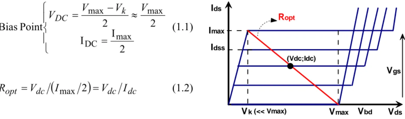
Assuming to operate in the simple case of a Class A amplifier, the quiescent bias point is fixed by the (1.1) and so, under the assumption of negligible knee voltage, it is half the
V
max; the load line theory says that to deliver the maximum power to the load both current (0ÆI
max) and voltage (0ÆV
max) swings must be maximized, staying up to their linear range (Figure 1.2) [4]. Clearly, the load line resistor in this optimum power matched condition has the value indicated in the (1.2).⎪ ⎩ ⎪ ⎨ ⎧ = ≈ − = 2 I I 2 2 Point Bias max DC max max V V V VDC k (1.1)
(
)
dc dc dc opt V I V I R = max 2 = (1.2) (Vdc;Idc) Ids Imax Idss Vk Vbd Vds Vgs (<< Vmax) Vmax RoptTheory of Microwave Power Amplifier 3 Applying their standard definitions to this idealized treatment, the output power and the efficiency assume the value below:
dc dc opt V I P = ⋅ 2 1 (1.3) 50% 2 1 100 100 = ⋅ ⋅ ⋅ = ⋅ = dc dc dc dc opt dc I V I V P P η (1.4)
It is clear that the ideal operating condition presented above is so far to be applied in a realistic power amplifier design, but we can consider it like a starting point for a more realistic treatment of the problem.
From all design amplifier theories is trivial that to enhance the efficiency the first step is to bias the active device to a low quiescent current and to allow the RF signal to swing the device into conduction. But the merely reduction of the conduction angle of an RF power amplifier is not sufficient in itself to give an useful improvement in efficiency; moreover it is also necessary to increase the drive level substantially from the Class A condition and to provide suitable impedance terminations at harmonics of the signal frequency, that become very important when the strong non linear regions are involved.
Defining
α
as the entire angle of conduction in the RF cycle, including the equal contributions on either side of the zero time point, Figure 1.3 shows as the reduction affects the current waveform, where, basing on the definition, the current cut-off points are at±α/2.
Figure 1.3 - Reduced conduction angle current waveform.
From the current waveform is intuitive that a reduction of the conduction angle implies a decreasing of the current mean component, or dc supply. Table 1.1 shows the definition of the classical modes of operation, in terms of quiescent bias point and conduction angle.
Mode Bias Point (Vq) Quiescent current Conduction angle
A 0.5 0.5 2π
AB 0 – 0.5 0 – 0.5 π - 2π
B 0 0 π
C < 0 0 0 - π
Table 1.1 - Classical Modes of Operation; Vq and Iq are normalized considering the threshold Vt=0 and the maximum voltage V0 =1.
To understand what happen to the fundamental component and to the harmonics is needful to perform the Fourier analysis of the RF current waveform, which can be written as indicated in the follows.
⎪⎩ ⎪ ⎨ ⎧ < < < < < < ⋅ + = π θ α α θ π α θ α θ 2 ; 2 - 0 2 2 cos ) q pk d I I (θ i q pk pk q I I I I I − = ⎟ ⎟ ⎠ ⎞ ⎜ ⎜ ⎝ ⎛ − = and max ) 2 cos(α
( )
[
cos cos 2]
) 2 cos( 1 ) ( max θ α α θ − − = I id (1.5)From the (1.5), integrating in the conduction period, the DC component and the magnitude of the nth harmonic of the drain current can be expressed like the (1.6) and the (1.7), while the DC and the fundamental components are determined in (1.8) and (1.9).
[
]
θ π α θ α α α d I Idc cos cos( ) ) cos( 1 2 1 2 2 max 2 2 − − =∫
− (1.6)[
]
θ θ π α θ α α α d n IIn cos cos( ) cos
) cos( 1 1 2 2 max 2 2 ⋅ − − =
∫
− (1.7) ) 2 cos( 1 ) 2 cos( ) 2 sin( 2 2 max α α α α π − − = IIdc (1.8) Result of (1.6) for DC component
) 2 cos( 1 sin 2 max 1 = I π −α− αα
I (1.9) Result of (1.7) for the fundamental frequency
Theory of Microwave Power Amplifier 5 The results from the evaluation of these integrals up to n=5 are shown in
Figure 1.4, where we can observe how the dc component decreases monotonically as
the conduction angle is reduced, while, affecting the strong nonlinearities, there is a growth of the harmonic components.
Amplitude (Imax=1) (CLASS) A AB B Conduction angle C 0 2π π 2nd 3rd 4th 5th DC Fundamental Amplitude (Imax=1) (CLASS) A AB B Conduction angle C 0 2π 2π π 2nd 3rd 4th 5th DC Fundamental
Figure 1.4 - Fourier analysis of reduced conduction angle mode
Just observing the graph above you can see that the reduction of the conduction angle from 2π (class A) to about π (class B) implies a reduction of the DC supply power while the RF fundamental component remains essentially the same, with a consequent improvement of the amplifier efficiency. Comparing the current values of both A and B classes, from the (1.8) and (1.9), we obtain that the efficiency raises form the 50% to the 78.5% (1.10). ) ( 2 ) 2 ( )
(ClassA I Imax I1 ClassA
Idc = dc π = = π π) max ( ) (ClassB I I Idc = dc = 2 ) ( max 1 ClassB I I = % 5 . 78 4 2 2 ) ( ) ( = = ⋅ = ⇒ = = η π η π π η η A B dc dc B A A I B I (1.10)
To complete the analysis about the effect of the reduction of the conduction angle on the amplifier performance we can see that for conduction angles lower than π, corresponding to class C operation, the dc continues to drop, but the fundamental
component of current also starts to drop below its class A level. This results in a higher efficiency but fundamental power lower then the class A rating of transistor.
From Figure 1.4, throughout the class AB range and up to the midway class B
condition, the only significant harmonics are the second one, in phase with the fundamental, and the third one, which is in anti-phase. As we will see in the next sections, an accurate control of load impedances at the harmonics is crucial for the optimization of the amplifier performances.
Instead of the drain efficiency (
η
), in the power amplifier design is more useful to consider the Power Added Efficiency (PAE); this index gives the opportunity to take into account not only the dc power supplied to the amplifier but also the RF input power, introducing the Gain as another important target in the trade-off of the performance. From this point of view, the best operating condition to optimize both output power and PAE is the Class AB operating mode.In the next paragraph, a simplified method for class AB design will be exposed.
1.2 Class AB Power Amplifier Design
The design of high-power and high-efficiency narrowband amplifiers implies a careful choice of bias point, loading and input power level. As we seen before, the choice of class A, AB, B or C is based on a compromise between gain, output power, efficiency and distortion contents [5]. Qualitative and quantitative considerations must therefore be made by the designer in order to obtain the best performances from a power stage [6-7]. In this paragraph general guidelines and a quick design procedure will be described.
The starting point of this analysis is the same simplified active device model shown in Figure 1.1. Power amplifier has to be output-matched with the conjugate of the large-signal output impedance in order to resonate the parasitic capacitances at the operating frequency; to do that, a “tuned” output circuit, which transfers the active power from the intrinsic transistor to the load, has been added to the model as shown in
Figure 1.5 [8]. We may therefore assume that voltage and current are in phase at the
intrinsic drain terminal; if we also assume a perfect resonator, or alternatively a short circuit load at higher harmonics, we may take the output voltage as a sinusoid.
Theory of Microwave Power Amplifier 7 Ids Gm•Vgs Cgs Ri Cpar Lload Rload 1 I R Vds = load ⋅ 0 I V Pdc = dd ⋅ 1 1 21V I P = ds ⋅ in P P G = 1 dc drain P P1 = η dc in P P P PAE = ( 1− ) (1.11) Figure 1.5 - Output tuned Circuit - Main Power Amplifier parameters
For given bias point and load resistance the output current waveform can be determined for every input power; from its Fourier coefficients
I
n, expressed in the (1.7), all the main power amplifier characteristics could be computed (1.11).From the
I
d– V
ds characteristic, plotted in Figure 1.6, we can assume the identification of the following physical parameters:V
k (drain saturation voltage),I
max (maximum drain current atV
gs=V
bi),V
bro (drain-source breakdown voltage withV
gs = 0) andV
p (pinch-off voltage); we can also consider as known the small-signal gain of the amplifier.Ids Idss Vk Imax Vgs= -Vp Vbr0 Vds GG Vgs= -V bi Vgs= -V Vgs= 0 Vbr VDC
Figure 1.6 - Output characteristics with a class AB Load Line.
Considering the electrical constrains for the operating conditions of the transistor, the Drain bias voltage can be expressed as:
2 ) 2 ( br0 k GG bi k dc V V V V V V = + − − ⋅ − (1.12)
Defining the working quantity
θ
, related to the ratio between the RF output voltage amplitude and the DC bias voltage, the bias current and the load resistance are related to this quantity and to the conduction angleα
through the (1.13) and the (1.14), whereR
s is the slope of the output characteristics in the ohmic region.)] sin( [ 1 )) 2 cos( 1 ( ) 1 ( 2 ) , ( α α α θ θ π θ α − ⋅ − ⋅ − ⋅ ⋅ = s load R R (1.13) ) 2 cos( 1 ) 2 cos( ) ( max α α α − − = I Idc (1.14) ⎥ ⎦ ⎤ ⎢ ⎣ ⎡ − = dc ds V V 1 θ
In figures 1.7b and 1.8 the output power and power-added efficiency, as computed from the model, are plotted Vs.
α
, withθ
as a parameter; by means of thesegraphs, the choice of the optimum
α
andθ
can be made. The behavior of the PAE isstrongly influenced by the gain of the transistor; therefore two cases for 9 and 12 dB small-signal gain are also reported.
60 80 70 3.143.5 4 4.5 5 5.5 6 6.28 α θ Rl oa d 0.1 0.125 0.15 0.175 0.2 0.225 90 110 100 130 120 150 140 158.4 56.5 60 80 70 3.143.5 4 4.5 5 5.5 6 6.28 α θ Rl oa d 0.1 0.125 0.15 0.175 0.2 0.225 90 110 100 130 120 150 140 158.4 56.5 a) 18 19 18.5 19.5 20.5 20 21 3.14 3.5 4 4.5 5 5.5 6 6.28 α θ Pou t [d Bm] 0.1 0.125 0.15 0.175 0.2 0.225 18 19 18.5 19.5 20.5 20 21 3.14 3.5 4 4.5 5 5.5 6 6.28 α θ Pou t [d Bm] 0.1 0.125 0.15 0.175 0.2 0.225 b) Figure 1.7 - Rload (a) and Pout (b) Vs. the conduction angle α, with θ as parameter.
Theory of Microwave Power Amplifier 9 0.4 0.45 0.55 0.5 0.6 3.14 3.5 4 4.5 5 5.5 6 6.28 α θ PA E 0.1 0.125 0.15 0.175 0.2 0.225 Gain = 9dB 0.4 0.45 0.55 0.5 0.6 3.14 3.5 4 4.5 5 5.5 6 6.28 α θ PA E 0.1 0.125 0.15 0.175 0.2 0.225 0.4 0.45 0.55 0.5 0.6 3.14 3.5 4 4.5 5 5.5 6 6.28 α θ PA E 0.1 0.125 0.15 0.175 0.2 0.225 Gain = 9dB a) 0.3 0.4 0.35 0.45 0.55 0.5 0.6 3.14 3.5 4 4.5 5 5.5 6 6.28 α θ PA E 0.1 0.125 0.15 0.175 0.2 0.225 Gain = 12dB 0.3 0.4 0.35 0.45 0.55 0.5 0.6 3.14 3.5 4 4.5 5 5.5 6 6.28 α θ PA E 0.1 0.125 0.15 0.175 0.2 0.225 Gain = 12dB b) Figure 1.8 - PAE Vs. the conduction angle α, with θ as parameter, for two different gain values.
From the plots, we can see that for decreasing
θ
(i.e. increasing load resistances)the output power decreases, but power-added efficiency increases because of the prevailing effect of the increased gain: at this point, the designer has to define the best compromise between the two. It is also apparent from the plots that the output power is weakly dependent on the circulation angle
α
(i.e. on the bias current), while the power-added efficiency is much more dependent; in particular the two contrasting effects of decreasing DC power dissipation and decreasing gain (going from class-A to class-B, i.e. fromα
= 6.28 toα
= 3.14) produce a clear maximum. Here again the choice of the compromise between best output power and best efficiency is left to the designer.Once the optimum
α
andθ
are chosen, the optimum bias and load resistance are easily computed from formula (1.14) above. At this point the actual values ofV
k andV
GG can be re-introduced into the formula forV
dc, and the procedure repeated; however, if the first guess was close to the final result, as is usually the case, only negligible readjustments are found. The design is therefore completed.1.3 Harmonic Tuned Power Amplifiers
The design approaches summarized above are based on the hypothesis of negligible or shorted harmonic frequency components. This assumption is not longer realistic in the design of high frequency and high power amplifiers, where the contribute of the harmonics becomes more influent and an accurate control of their terminations is
a crucial target for designers [9-11]. This paragraph explains some basic information about the design of high power and high efficiency power amplifiers basing on the harmonic tuning of the load impedances [12].
From the (1.15), derived from a simple power balance consideration, it’s clear that, to maximize the drain efficiency, at least one of the two following equivalent conditions have to be satisfied: (a) maximize the fundamental output power
P
out,f or minimize both output harmonic terminations (P
out,nf, n>1) and the dissipated power on the device (P
diss). Since the target of the following analysis is to provide a useful design mean, it is easier to manage the former condition instead of the latter.
∑
> + + = = 1 , , , , n nf out f out diss f out dc f out P P P P P P η (1.15)Assuming the active device as a voltage controlled source, as indicated in
Figure 1.5, maximization of the fundamental output power corresponds to the
maximization of the fundamental drain voltage component, with the constraint that the resulting voltage waveform has to be physically consistent. Assuming a periodic steady state, the drain current and the drain voltage waveforms can be expressed as the (1.16) and (1.17) respectively, where the limitations due to the intrinsic characteristics of the active device and the circuit complexity limit the output harmonic terminations control up to 3f. If the output harmonic terminations are assumed as purely resistive, the voltage and current components can be related by the (1.18).
∑
∞ = ⋅ + = 1 0 cos( ) ) ( n n ds t I I n t I ω (1.16)[
cos( ) cos(2 ) cos(3 )]
) (t V V1 t k2 t k3 t vds = dd − ⋅
ω
+ ⋅ω
+ ⋅ω
(1.17)⎥
⎥
⎥
⎥
⎦
⎤
⎢
⎢
⎢
⎢
⎣
⎡
=
=
1 3 3 1 2 2V
V
K
V
V
K
n n nf L VI R , = (1.18)Then, for a fixed
I
n, the maximization of the efficiency is transformed in the selection of the two parameters k2 and k3 values maximizingV
1, with the condition that the drainTheory of Microwave Power Amplifier 11 voltage is maintained lower than the breakdown. The results of this problem are summarized in the following table [13].
Controlled Frequencies k2 k3 δ β Achievable V1 f Tuned Load 0 0 1 1 Vdd f, 3f Class F 0 -0.17 1.15 1 1.15 - Vdd f, 2f 2nd h. tuning -0.35 0 1.41 1.91 1.41 - Vdd f, 2f, 3f Class FG -0.55 0.17 1.62 2.8 1.62 - Vdd
Table 1.2 - Results obtainable with different Harmonic control.
In the table above, the quantity
δ
(Voltage Gain Function) relates the fundamental drain voltage amplitudeV
1, obtainable by proper harmonic terminations, to the bias voltageV
dd, that can be considered as the fundamental amplitude for the unmanipulated approach (TL case); the Voltage Overshoot Function,β
, quantifies the overshoot phenomena due to the use of even harmonic components. The two figures are defined as: dd V V k k2, 3) 1 ( = δ ; dd ds V t v k k , ) max[ ( )] ( 2 3 = β (1.19)The
δ
function directly gives the improvement on drain efficiencyη
with respect to the Tuned Load (TL) case. However, theδ
values have to be considered carefully, not to violate physical constraints. In fact, since drain voltage harmonic componentsV
n are generated by the current harmonic ones,I
n, through the drain impedancesR
L,nf (1.18), thek
2 andk
3 optimum values must be physically synthesized, i.e. the corresponding impedancesR
L,2f andR
L,3f must be positive values.I
2 andI
3 have therefore to satisfy proper phase relationships with respect toI
1 (Table 1.2, sign ofk
2 andk
3). Such relationships are very important, since if not fulfilled may lead to detrimental results.These analytical results are at the base of the design approaches discussed in this thesis, because they directly influence the load line shape; in fact, as we will see in next
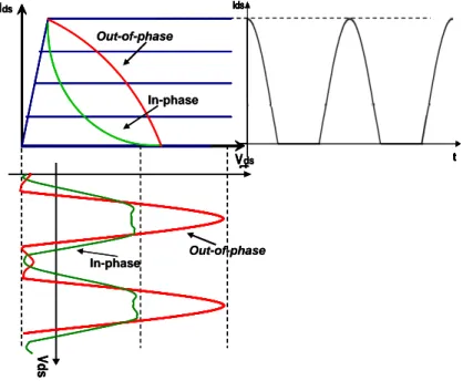
chapters, a proper control of the shaping of the Load Line at the intrinsic terminals of the active device allows optimizing the power amplifier’s performances.
t Ids t Ids Ids Vds Vds t In-phase Out-of-phase Out-of-phase In-phase t Ids t Ids Ids Vds Vds t t Ids t Ids Ids Vds Vds t In-phase Out-of-phase Out-of-phase In-phase
Figure 1.9 - Output load curve for 2nd harmonic tuning approach with proper (out-of-phase) or wrong (in-phase) voltage components
Optimum load impedances for the intrinsic drain current source can be determined as the (1.20). Thus, the harmonic “output” approach can be useful if the generated drain current waveform allows positive values for
R
L,nf, according to that equation. In fact, even if there is a power dissipation on such harmonic loads, that could be interpreted as a detrimental phenomena, the fundamental output power is maximized, simultaneously maximizing the drain efficiency.1.4 The Load-Pull Techniques
In the advanced design of high power amplifiers, the Load-Pull technique represents a powerful tool to search and to synthesize proper load impedances, taking into account the needful trade-off between several amplifier's characteristics. This method is based on the definition of the active device performances for different load impedances and, then, for different points on the smith chart. In this way, closed contours can be plotted on the chart, marking the boundaries of specified levels of output power, efficiency, gain, etc., (Figure 1.10) [14]. For example, if the target of the
Theory of Microwave Power Amplifier 13 design is a compromise between minimum levels of both output power and efficiency, superimposing on the same graph their contours, the designer can chose the particular impedance for which both conditions are satisfied.
P_max PAE_max
P_max PAE_max
Figure 1.10 - Typical Load Pull contours for power and efficiency.
The Load Pull technique can be applied by different approaches: one is based on large signal simulations, the other on measurements and experimental results. In the former case, a full non linear model for active device is needed, joined with non linear analysis algorithms. For this approach, the major drawbacks are related to the use of an appropriate and accurate non linear model [15-16] and to the complexity of the computation in the design CAD tools when strong levels of non linearity have to be reached.
The experimental approach is based on Load Pull systems, in which the active device is fully characterized in terms of output power, matching impedances, efficiency, and any other required performance, by means of exhaustive and intensive measurement activity [17-20]. At the moment there are two different kinds of Load Pull systems, the active one and the passive one, basing on an active or a passive load synthesis. For the purpose of this work, in this paragraph, a brief description of the only passive Load Pull bench will be exposed.
Figure 1.11 shows a typical Load Pull setup, where both Source and Load
impedances of the DUT are synthesized and modified by means of two Programmable
Tuners. This setup allows measuring the main characteristics of the DUT for different
load conditions and then producing, by specific software, the needed Load Pull contours. Such a system provides a complete large-signal characterization of the DUT
to the designer, which can chose the proper input and output impedances to satisfy the required performances.
Source 1 Source 2 Power Supply Dual Channel Power Meter Spectrum Analyzer BT BT Driver Amp. Combiner/Coupler Isolator
Source Tuner Load Tuner
Wafer Probe Station DUT
Co
upler
Source 1 Source 2 Power Supply Dual Channel Power Meter Spectrum Analyzer BT BT Source 1 Source 2 Power
Supply Dual Channel Power Meter Spectrum Analyzer BT BT Driver Amp. Combiner/Coupler Isolator
Source Tuner Load Tuner
Wafer Probe Station DUT
Co
upler
Figure 1.11 - Typical Passive Load Pull Setup.
The Active Load Pull systems have the same target of the passive one, that is to synthesize a wide range of impedances at the input or output of the DUT, but the main difference is in using a “virtual load”: part of the outgoing signal is modified in amplitude and phase by amplifier/phase shifter network and re-injected into the output port the DUT. The device sees a load reflection factor that could be equal or larger than 1, because amplifier is involved, compensating for the loss of cable and test fixtures, and then covering every impedances in the smith chart plane.
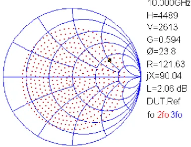
However, also load-pull setups, both active and passive, present some relevant drawbacks; first of all they are frequency and power limited, and their cost dramatically increases when high operating power and/or frequencies are required. Then, a major limitation of this technique is related to the difficulty in synthesizing the full range of device terminations: especially when on-wafer devices having a large periphery are considered, passive load-pull suffers from the inability to synthesize very low impedances (Figure 1.12), whereas active load-pull may become critical from the stability point of view. Moreover, once load-pull contours have been drawn, no information is given about the intrinsic ED Load Line, that, as explained in the paragraphs above, plays a fundamental role in the design activity: loading conditions which show similar microwave performance can correspond to very different Load Lines at the intrinsic device. This is a vital aspect since reliability conditions are defined
Theory of Microwave Power Amplifier 15 at the intrinsic ED ports [21] as the passive access structures to the active area do not have any major impact on reliability (for instance, the device breakdown condition is related to the breakdown of the intrinsic gate-drain diode).
Figure 1.12 - Typical map of the achievable impedances in a passive load pull system. The figure above shows a typical map of the impedances achievable by a Passive Load Pull system at 10 GHz, where the minimum input impedance which can be synthesize has a reflection coefficient of about 0.75.
1.5 Summary
In this chapter, the theories, that represent the pillar of the power amplifier design techniques, have been summarized. In particular, we saw as such a kind of circuits is usually designed by exploiting a mix of three different approaches: Cripps load-line theory, load-pull measurements, and iterative harmonic-balance analyses based on nonlinear models of electron devices (ED).
Furthermore, basing on these theories, the main approaches for the definition of the best load impedances for high efficiency high power amplifiers have been explained, focusing on the fundamental role of the harmonic tuning in the optimization of both output power and Power Added Efficiency.
Theory of Microwave Power Amplifier 17
References
[1] S. Marsh, “Practical MMIC Design.” Norwood, MA: Artech House, 2006.
[2] F. Giannini, G. Leuzzi, “Nonlinear Microwave Circuit Design.” Chichester, England: Wiley, 2004.
[3] S. C. Cripps, “RF Power Amplifiers for Wireless Communication”, Norwood, MA: Artech House, 1999.
[4] H. Kondoh, “FET Power Performance Prediction Using a Linearized Device Model”, 1988 IEEE MTT-S Symposium Digest, pp. 569-572.
[5] L.J. Kushner, “Output Performance of idealized Microwave Power Amplifiers”, Microwave Journal, n.10, October 1989, pp. 103-116.
[6] D.M. Snider, “A Theoretical Analysis and Experimental Confirmation of the Optimally
Loaded and Overdriven RF Power Amplifier”, IEEE Transactions on Electron Devices,
Vol. ED-14, Dec.1967, pp. 851-857.
[7] G. Halkias, H. Gerard, Y. Crosnier and G. Salmer, “A New Approach lo the RF Power
Operation of MESFET’s”, IEEE Trans. Microwave Theory Tech., vol. 28, n. 11, November
1989, pp. 1157-1163.
[8] F. Giannini, G. Leuzzi, E. Limiti, “Class-AB Power Amplifier Advanced Design
Techniques”, SBMO/IEEE MTT-S IMOC'95 Proceedings, Vol. 1, July 1995, pp. 361-368.
[9] M.Maeda et al., “Source Second-Harmonic Control for High Efficiency Power Amplifiers”, IEEE Trans. on Microwave Theory and Techniques, Vol.MTT-43, n.12, December 1995, pp.2952-2958.
[10] S.R. Mazumder, A. Azizi, F.E. Gardiol, “Improvement of a Class-C Transistor Power
Amplifier by Second-Harmonic Tuning”, IEEE Trans. on Microwave Theory and
Techniques, Vol. MTT-27, n. 5, May 1979, pp.430-433.
[11] S. Watanabe et al., “Simulation and Experimental Results of Source Harmonic Tuning on
Linearity of Power GaAs FET Under Class AB Operation”, 1996 IEEE MIT-S Symposium
Digest, pp. 1771-1777.
[12] P. Colantonio, F. Giannini, G. Leuzzi, E. Limiti, “Harmonic Tuned PAs Design Criteria”, Microwave Symposium Digest, 2002 IEEE MTT-S International, Vol. 3, 2-7 June 2002, pp.1639 – 1642.
[13] P. Colantonio, F. Giannini, G. Leuzzi, E. Limiti, “Multi Harmonic Manipulation for Highly
Efficient Microwave Power Amplifiers”, Int. Journal on RF and Microwave CAE, Vol.11,
N. 6, Nov. 2001, pp. 366-384.
[14] S.C.Cripps, “A Theory for the Prediction of GaAs FET Load-Pull Power Contours”, 1983, IEEE MTT-S Digest, pp 221-333.
[15] M. Hirose, Y. Kitaura, and N. Uchitomi, “A large-signal model of self-aligned gate GaAs
FET’s for high-efficiency power-amplifier design”, IEEE Trans. Microwave Theory Tech.,
Vol. 47, Dec. 1999, pp.2375–2381.
[16] W. Ce-Jun, Y. A. Tkachenko, and D. Bartle, “A new model for enhancement-mode power
pHEMT”, IEEE Trans. Microwave Theory Tech., Vol. 50, Jan. 2002, pp. 57–61.
[17] J.M. Cusak, S.M. Perlow, B.S. Perlman, “Automatic load contour mapping for microwave
power transistors”, IEEE Trans. On Microw. Theory and Tech., Vol. 22, n. 12, Dec. 1974,
pp.1146-1152.
[18] A. Ferrero, V. Teppati, “Accuracy Evaluation of On-Wafer Load-Pull Measurements”, in Proc. IEEE 55th ARFTG Microwave Measurements Conference, Boston, 2000, pp. 1–5. [19] Focus Microwaves Data Manual, Focus Microwaves Inc., Montreal, Canada, 1988.
[20] M.N. Tutt, D. Pavlidis, C. Tsironis, “Automated On-Wafer Noise and Load Pull
Characterization Using Precision Computer Controlled Electromechanical Tuners”, in
Proc. IEEE 37th ARFTG Microwave Measurements Conference, Boston, 1991, pp. 66–75. [21] A. Raffo, V. Di Giacomo, P.A. Traverso, A. Santarelli, G. Vannini, “An Automated
Measurement System for the Characterization of Electron Device Degradation under Nonlinear Dynamic Regime”, IEEE Trans. Instrum. Meas., to be published.
19
Chapter 2
Design of Hybrid HPA for Space
Applications
In the previous chapter, the main design methodologies for power amplifiers were presented, starting with the more theoretical one and, then, describing the more experimental approaches. The evolution of these methods has been applied to develop very different techniques for design of power amplifiers for different kinds of applications. The main purpose of the research activity described in this thesis is the definition and application of a quite simple design methodology capable to produce the best performances but, at the same time, satisfying the tight constrains imposed by space applications.
In this chapter, after a description of the motivations for that constraints required by satellite systems, the proposed methodology will be explained by means of the design of a hybrid high power amplifier to be used in a SAR (Synthetic Aperture Radar) antenna. The final results will be the realization of a TR module representing the state of the art in this particular field of application.
2.1 Effects of Space constrains on power amplifier design
It is trivial to understand that a very crucial point for every kind of space system is the reliability. That is not just because, after the launch, any maintenance operation is not possible but also for the sever environment conditions in which the system has to work. The reliability issues involve every component of the vehicle, both mechanical and electrical; concerning the power amplifiers or, more in general, the overall TR module, designer has to taking into account how the space constraints engrave on the times of life and on the performances of the electronics components but, also, how the mechanical limitations, for example on the bonding wires, have influence on the degrees of freedom of the entire project.
To assure proper reliability levels, each component of satellite equipment has to operate in “derating” conditions, defined by the agencies for space standardization [1]. The term derating refers to the intentional reduction of electrical, thermal and mechanical stresses on components to levels below their specified rating. Derating is a means of extending component life, increasing reliability and enhancing the end-of-life performance of equipment. It provides a safety margin between the applied stress and the demonstrated limits of the component capabilities. In addition, derating participates in the protection of components from unexpected application anomalies and board design variations. Derating requirement shall be taken into account at the beginning of the design cycle of equipment for any consequential design trade-off to be made.
Concerning power amplifier design, derating has to be applied to both temperature and electrical limits recommended by the foundry for both active and passive structures, engraving, certainly, on the circuit’s performances. This means that, during design activity, several factors must be kept carefully under control; some of them are listed below:
– Junction temperature at maximum operating conditions; – Power rating and dissipation;
– Maximum voltage and current;
In particular, while the channel temperature of active devices is tightly linked to its MTBF (Mean Time before Failure), current and voltage levels have to be compared to the most destructive phenomena of breakdown. Conjecturing that, as usually happen, designer has to apply a derating of the 20% respect of the maximum rating provided by
Design of Hybrid HPA for Space Applications 21 the foundries, it means that he has a reduction of the maximum dynamic swing for both currents and voltages, with a consequent abatement of the maximum deliverable power.
The component parameter strength defines the limits and the performance component technology in the particular application and varies from manufacturer to manufacturer, from type to type, and from lot to lot and can be represented by a statistical distribution. Likewise, component stress can be represented by a statistical distribution. Figure 2.1 illustrates the strength of a component and the stress applied at a given time, where each characteristic is represented by a probability density function. A component operates in a reliable way if its parameter strength exceeds the parameter stress. The designer shall strive to make sure that the stress applied does not exceed the component parameter strength. This is represented by the intersection (shaded area) in the picture. The larger the shaded area, the higher the possibility of failure becomes.
Figure 2.1- Parameter stress vs. strength relationship.
There are two ways, which may be used simultaneously, in which the shaded area can be decreased:
• Decrease the stress applied (which moves the stress distribution to the left).
• Increase the component parameter strength (by selecting over-sized components) thereby moving the strength distribution to the right.
The goal is to minimize the stress-to-strength ratio of the component. Derating moves the parameter stress distribution to the left while the selection processes applied to the components for space applications contribute to moving the parameter strength distribution to the right. The selection processes also reduce the uncertainty associated with the component parameter strength. Derating reduces the probability of failure,
improves the end-of-life performance of components and provides additional design margins. Another effect of derating is to provide a safety margin for design. It allows integrating parameter distribution from one component to another and from one procurement to another.
2.2 HPA - Application context
To define a design methodology capable to maximize the performance of power amplifiers for space applications, complying the tight constrains, an HPA has been studied and developed, to be used in a L-band TR module for a SAR (Synthetic
Aperture Radar) antenna for earth observation (Figure 2.2).
Φ
PS VA Pre-driver driver
HPA
Φ
PS VA buffer LNA limiter
SW
Φ
PS VA Pre-driver driver
HPA
Φ
PS VA buffer LNA limiter
SW
Figure 2.2 - Schematic of a TR module.
Synthetic aperture radar can provide measurements key to the water cycle (e.g. soil moisture and water level), global ecosystem (biomass estimation, land cover change), and ocean circulation and ice mass (ice motion). L-band radar provides the ability to make these measurements under a variety of topographic and land cover conditions, day or night, with wide coverage at fine resolution and with minimal temporal de-correlation [2, 3]. L-band is the preferred frequency for land-related studies because the wavelength favours long-term correlation, is less sensitive to ionospheric disturbances and has sufficient frequency allocated bandwidth. For all these reasons, L-band represents an important segment for many space programs world-wide [4-6] Electronically-steered phased array antennas are required for beam agility to enable rapid accessibility, global coverage and short revisit times [7].
Design of Hybrid HPA for Space Applications 23 Space-based radar places significant demands on the spacecraft resources (mass, power, data rate) and is therefore very expensive to implement. These systems typically require active phased-array antennas with hundreds or thousands of Transmit/Receive (T/R) modules distributed on the array. High Efficiency is a vitally important figure of merit for the radar T/R module because it reduces the power consumption and therefore makes best possible use of the limited power available. High efficiency also improves the thermal design and reliability. Beside efficiency, high output power is also requested to reduce the number of the modules, and then mass and space, and to enhance the SAR performance and the system service capability [8].
In order to reach the state of the art in this filed, the target of the design activity has been to realize an HPA capable to deliver an output power of about 40 Watts with a Power Added Efficiency (PAE) better than the 40% and fully compliant with the space application constrains. To reach such levels of power at this relatively low frequency, the Hybrid is the only possible solution, based on the combination of discrete active devices, lamped components and microstrip structures on high frequency laminates.
2.3 HPA Design
The starting point of the design activity is a proper choice of the technology to be used, basing on the design specifications and on the availability of a space qualified process. Basically, the available technologies for that application are Silicon LDMOS and Bipolar, GaAs FET, GaAs HFET, GaAs pHEMT and GaInP HBT. The frequency of the application, the requested power and efficiency levels, the thermal constrains and the reliability issues impose to choose a GaAS pHEMT process, the only one capable to make a trade-off between all that conditions.
After a preliminary study of all possible solutions, a space qualified 0.35-um gate length GaAs p-HEMT process from Triquint Semiconductors Texas has been identified as the best solution for this application. This process is characterized by a VDS breakdown exceeding 24 Volts, a maximum current density of 650 mA/mm and it can reach 1.2 W/mm power density at 10 GHz at maximum ratings; due to the space application constraints, the HPA performances must be obtained using devices at de rated conditions. For this application these were identified as 20% de-rating on
breakdown voltages and current densities. As mentioned above, the only viable approach identified is represented by the hybrid combination of 4 discrete high power
bar, realized by the union of some pHEMT basic active cells (Figure 2.3) [9].
12-mm Discrete
Power Bar
8 x 1.5-mm
basic cells
0.595mm x 2.93mmFigure 2.3 - The adopted 0.35µm pHEMT discrete bar: 8 unit cells (1.5 mm periphery each) for a total 12 mm gate periphery.
The power bar, in figure above, is composed of 8 pHEMT cells of 1.5 mm periphery each for a total gate periphery of 12 mm: this is the largest discrete device available as foundry standard product. The 8 cells are combined with a very high packing density: all the drains and the gates are connected on chip in a bus-bar like solution and are then, to a good extent, equipotential. Moreover, 8 gate and drain pads are available for wire bonding for a uniform distribution of the RF signal along the big periphery device. At maximum ratings condition this discrete pHEMT is rated to deliver
14 Watt output power at 10 GHz. However these performances can’t be achieved
applying the de-rating rules required for space application, which are in particular 20% de-rating on breakdown voltages and current densities, and maximum channel temperature below 120°C, despite of the 150°C suggested by the foundry to obtain the same MTBF.
The design focus is on the choice, for the elementary cell, of a proper bias and dynamic load-line which are able to optimize circuit performances like power and efficiency within the de-rated operating conditions. Taking into account the existing design methods presented in the Chapter 1, the approach explained below is based on a proper control and shaping of the dynamic load-line, monitored at the intrinsic terminals of the active device; imposing a particular shape to the load-line, a trade-off between power and efficiency can be reached and, at the same time, electron device currents and voltages related to reliability issues can be directly monitored.
Design of Hybrid HPA for Space Applications 25 Single Cell Design
As said before, the elementary cell, composing the power bar, has a total gate periphery of 1.5 mm (10 gate fingers x 150 um width); optimizing the foundry design kit models for L band by means of linear and non-linear (load pull) measurements on some samples, the non linear model for the device was perfected and used in a simulation CAD tools for design.
The need to maintain the channel temperature of the device below 120°C, for each electrical condition and at the maximum ambient temperature of about 40°C, and to work in a high efficiency condition, imposes to choose the AB class as the operating condition of the amplifier, corresponding to the quiescent Bias values indicated in the table below.
Quiescent Bias Point
V
ds= 10 V
I
ds= 113 mA
V
gs= -0.625 V
Table 2.1 - Polarization values of the single active cell of the HPA.
Considering that for this technology, in maximum rating conditions, the Drain-Source breakdown voltage could exceed about 24 Volts, the
V
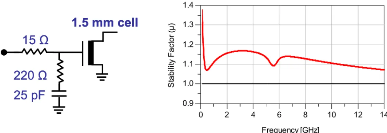
ds of 10 V allows to comply the derating of 20% imposed by the application.The active device is made unconditionally stable, form DC to cut-off frequency, by mean of a combined series-shunt RC stabilizing network, ensuring a good trade-off with the achievable gain. Figure 2.4 shows a schematic of that network and its effects on the stability factor
µ.
25 pF
220 Ω
15 Ω
1.5 mm cell
25 pF
220 Ω
15 Ω
1.5 mm cell
2 4 6 8 10 12 0 14 1.0 1.1 1.2 1.3 0.9 1.4 Frequency [GHz] S ta b ilit y F a ct o r ( µ )After the unconditional stabilization has been assured, the next and the most important step is to define the optimum impedance load for the device; that is the
Γ
L (Figure 2.5) which allows reaching the required performances in terms of output power and efficiency and the needed level of reliability, at the central frequency of 1.275 GHz.Output
Output
Network
Network
Input
Input
Network
Network
Γ
LΓ
S50Ω
Active
Cell
Z
sOutput
Output
Network
Network
Input
Input
Network
Network
Γ
LΓ
S50Ω
Active
Cell
Z
sFigure 2.5 - Schematic of PA structure.
As said before, the method is based on a proper shaping of the dynamic load-line evaluated at the intrinsic terminals of the Electron Device (ED). As Figure 2.6 shows, after the definition of the optimum impedance at intrinsic terminals (
Z
Lin), which are accessible for the model used, the impedance to be synthesized by the output network (Z
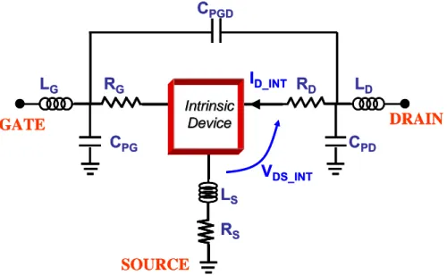
L) can be obtained adding the effects of the parasitics network.Intrinsic Intrinsic Device Device RD LD CPD RG LG CPG RS LS DRAIN GATE SOURCE VDS_INT ID_INT CPGD Intrinsic Intrinsic Device Device RD LD CPD RG LG CPG RS LS DRAIN GATE SOURCE VDS_INT ID_INT CPGD
Figure 2.6 - Schematic of the electrical model used to design. Intrinsic Device and parasitic elements are pointed out.
Design of Hybrid HPA for Space Applications 27 The starting point is to define an appropriate
Z
L, at fundamental frequency, in order to compensate the phase shifting between the drain current and voltage, due to then nonlinear capacity CDS, and try to reach, at the same time, both saturation and interdiction zones. While the former condition, recognizable by the rectification of the load-line, allows to reduce reactive contributions to the power, the latter one, as viewed before, allows to maximize both current and voltage swing, improving the power level. Figures below show the first choice of the load impedance (Z
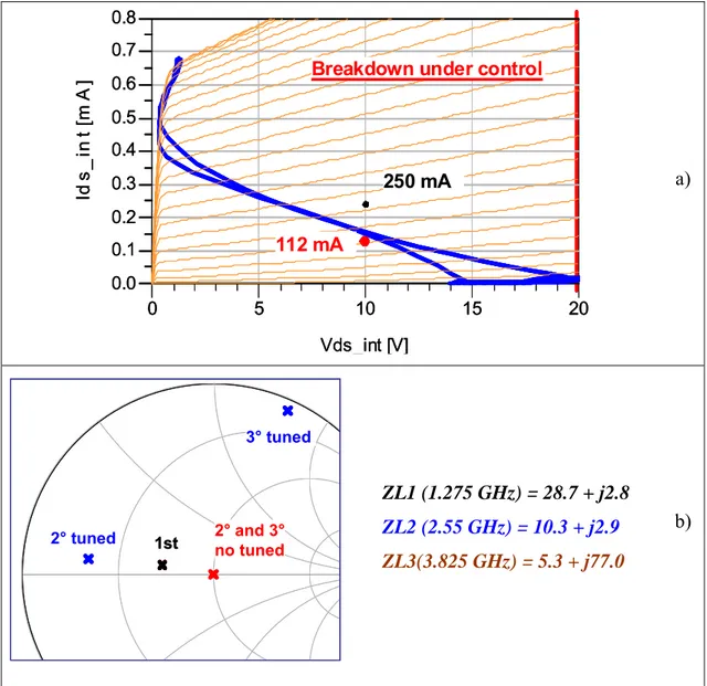
L1), without any operation at the harmonic components, the relative load-line superimposed on the pulsed I-V characteristics and main performances of the single active cell in an operating condition relative at a gain compression of about 2.8 dB.5 10 15 0 20 0.1 0.2 0.3 0.4 0.5 0.6 0.7 0.0 0.8 Vds_int [V] Id s_ in t [A ] 112 mA 247 mA
Breakdown under control
5 10 15 0 20 0.1 0.2 0.3 0.4 0.5 0.6 0.7 0.0 0.8 Vds_int [V] Id s_ in t [A ] 112 mA 247 mA 5 10 15 0 20 0.1 0.2 0.3 0.4 0.5 0.6 0.7 0.0 0.8 Vds_int [V] Id s_ in t [A ] 112 mA 247 mA
Breakdown under control
Figure 2.7 - First solution for the intrinsic dynamic Load-Line corresponding to ZL1. As the picture shows, at large signal condition the operating current rises from
112 mA to 247 mA, due to the auto-biasing phenomena, but, at the same time, there is a
shifting of the dynamic load-line to a more dissipative region; that implies, as demonstrate in Figure 2.8, a not best condition for both efficiency and temperature. Beside the relative performances, Figure 2.7 explains the importance of monitoring the intrinsic load-line, because the designer can monitor the drain voltage does not reach, dynamically, the breakdown limits.
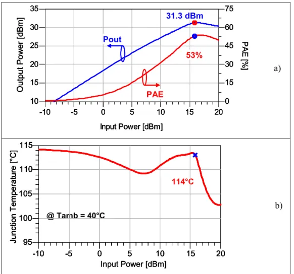
Figure 2.8 shows the output power, the PAE and the junction temperature in
compression, the single active device could deliver a power of about 31.3 dBm, with the
53% of PAE and a maximum channel temperature of about 114°C.
-5 0 5 10 15 -10 20 15 20 25 30 10 35 15 30 45 60 0 75 Input Power [dBm] PAE [ % ] Out put P o w e r [dB m ] 31.3 dBm 53% PAE Pout -5 0 5 10 15 -10 20 15 20 25 30 10 35 15 30 45 60 0 75 Input Power [dBm] PAE [ % ] Out put P o w e r [dB m ] -5 0 5 10 15 -10 20 15 20 25 30 10 35 15 30 45 60 0 75 Input Power [dBm] PAE [ % ] Out put P o w e r [dB m ] 31.3 dBm 53% PAE Pout a) 114°C @ Tamb = 40°C -5 0 5 10 15 -10 20 100 105 110 95 115 Ju nc tio n T emp er at ur e [°C ] Input Power [dBm] 114°C @ Tamb = 40°C -5 0 5 10 15 -10 20 100 105 110 95 115 Ju nc tio n T emp er at ur e [°C ] Input Power [dBm] -5 0 5 10 15 -10 20 100 105 110 95 115 Ju nc tio n T emp er at ur e [°C ] -5 0 5 10 15 -10 20 100 105 110 95 115 Ju nc tio n T emp er at ur e [°C ] Input Power [dBm] b)
Figure 2.8 - Output Power, PAE (a) and Junction Temperature (b) for the 1.5mm single cell for a load impedance corresponding to ZL1.
In these conditions, the efficiency can be improved, preserving the same level of power, forcing the load-line to work in a less dissipative region, reaching, anyway, the maximum levels of both drain current and voltage. To give to the load-line this particular shaping a harmonic tuning has to be performed, choosing appropriate values for the second and the third harmonics of the load impedance (respectively
Z
L2 andZ
L3).Figure 2.9 shows as, starting from the standard condition with shorted harmonics, the proper tuning of
Z
L2 andZ
L3 allows to give the desired shape to the load-line, confirmed by an enhancement of about three percentage points in terms of PAE and by a very good level of the output power (Figure 2.10a). Working in moreDesign of Hybrid HPA for Space Applications 29 efficient conditions, also a reduction of the channel temperature can be observed (Figure 2.10b). 5 10 15 0 20 0.1 0.2 0.3 0.4 0.5 0.6 0.7 0.0 0.8 Vds_int [V] Id s _ in t [m A ] 112 mA 250 mA
Breakdown under control
5 10 15 0 20 0.1 0.2 0.3 0.4 0.5 0.6 0.7 0.0 0.8 Vds_int [V] Id s _ in t [m A ] 112 mA 250 mA
Breakdown under control
a) 1st 2° and 3°no tuned 2° tuned 3° tuned 1st 2° and 3°no tuned 2° tuned 3° tuned ZL1 (1.275 GHz) = 28.7 + j2.8 ZL2 (2.55 GHz) = 10.3 + j2.9 ZL3(3.825 GHz) = 5.3 + j77.0 b)
Figure 2.9 - Harmonic tuned dynamic Load-Line (a); Load Impedance at fundamental, second and third harmonic.
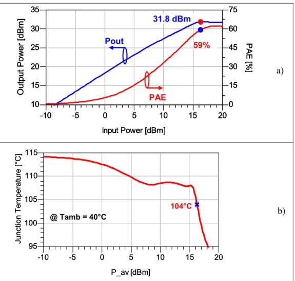
Figure below shows as, after harmonic tuning, the Power Added Efficiency rises up to 59%, with an output power of about 31.8 dBm, and the junction temperature decreases to 104°C.
-5 0 5 10 15 -10 20 15 20 25 30 10 35 15 30 45 60 0 75 Input Power [dBm] PAE [ % ] O u tput P o w e r [dBm ] 31.8 dBm 59% PAE Pout -5 0 5 10 15 -10 20 15 20 25 30 10 35 15 30 45 60 0 75 Input Power [dBm] PAE [ % ] O u tput P o w e r [dBm ] -5 0 5 10 15 -10 20 15 20 25 30 10 35 15 30 45 60 0 75 Input Power [dBm] PAE [ % ] O u tput P o w e r [dBm ] 31.8 dBm 59% PAE Pout a) -5 0 5 10 15 -10 20 100 105 110 95 115 P_av [dBm] Ju nc tio n Te m pe ra tur e [° C] 104°C @ Tamb = 40°C -5 0 5 10 15 -10 20 100 105 110 95 115 P_av [dBm] Ju nc tio n Te m pe ra tur e [° C] 104°C @ Tamb = 40°C b)
Figure 2.10 - Output Power, PAE (a) and Junction Temperature (b) for the 1.5mm single cell for the tuned load impedance.
The comparison between the two load-lines of figures 2.7 and 2.9 is at the base of the proposed approach. Imposing a proper shape to the load-line, the designer can perform the desired trade-off between the target performances and, at the same time, the electrical quantities that affect the reliability can be kept under control. In this particular case, where the target is design a HPA with high power and high efficiency, a sinking of the load-line in a region at lower dissipation, by mean of harmonic tuning, it gives a substantial improvement to the efficiency. In other cases, when, for example, linearity is researched, the target is to maintain the line as straight as possible.
Design of Hybrid HPA for Space Applications 31
Discrete Power Bar Performances
The optimum load conditions defined for the single active device have to be scaled for the entire Power Bar, with a total gate periphery of 12mm realized by the combination of 8 elementary cell of 1.5 mm (Figure 2.11).
Gate pads Drain pads
Gate pads Drain pads
Figure 2.11 - The adopted 0.35um pHEMT Discrete Power Bar.
Basing on the performances obtained for the single cell, the entire Power Bar should deliver, at 1.275 GHz, a total output power of about 12 Watts. Simply scaling
from the single cell, the quiescent Bias point becomes: VDS=10V, IDS=900mA and
VGS=-0.625V, with the current that, at large signal conditions, has to rise up to 1.9A.
Figure 2.12 shows the load impedance for the entire Bar, at both fundamental and
harmonic frequencies; that impedance has to ensure each of the elementary devices to be loaded in the optimum condition described above, preserving, hence, the optimum load-line.
1
st
2
nd
3
rd
1
st
2
nd
3
rd
ZL1 (1.275 GHz) = 6.7 + j0.6 ZL2 (2.55 GHz) = 0.5 + j0.1 ZL3(3.825 GHz) = 0.3 + j7.5As plotted in the figure below, the Power Bar should deliver an output power of about 12 W, preserving the same efficiency of the single cell, 59%.
TJ [C] 104.070 5 10 15 20 25 30 35 0 40 20 25 30 35 40 15 45 20 40 0 60 Potenza disponibile [dBm] Po u t [ d Bm ] PAE [ % ] a n d G a in [d B] Outp ut P ow e r [dB m ] Input Power [dBm] PAE [ %] and G a in [d B] Tj = 104 °C PAE Gain Pout TJ [C] 104.070 5 10 15 20 25 30 35 0 40 20 25 30 35 40 15 45 20 40 0 60 Potenza disponibile [dBm] Po u t [ d Bm ] PAE [ % ] a n d G a in [d B] Outp ut P ow e r [dB m ] Input Power [dBm] PAE [ %] and G a in [d B] Tj = 104 °C PAE Gain Pout Pout = 40.8 dBm PAE = 59.2 % Gain = 15 dB
Figure 2.13 - Simulated Performances for the Power Bar.
A verification that single cells work properly inside the Power Bar is given by the waveforms of both drain current and voltage plotted in Figure 2.14; the maximum and minimum levels of the two quantities are the same evident from the load-line in
Figure 2.9, and the clipping of the voltage curve denotes that devices are working in a
high efficiency condition.
0.2 0.4 0.6 0.8 1.0 1.2 1.4 0.0 1.6 5 10 15 20 0 25 0 200 400 600 -200 800 Time [nS] In tr in si c V d s [V ] Intr in si c Id s [m A ] Vds Ids Breakdown Limit 0.2 0.4 0.6 0.8 1.0 1.2 1.4 0.0 1.6 5 10 15 20 0 25 0 200 400 600 -200 800 Time [nS] In tr in si c V d s [V ] Intr in si c Id s [m A ] Vds Ids Breakdown Limit
Design of Hybrid HPA for Space Applications 33
2.4 Experimental Verifications
Results explained above are based just on theory and CAD simulations; even if the used electrical models have been verified by small and large signal measurement, a wide experimental activity was performed in order to verify the goodness of the design approach, taking into account all the unavoidable limits imposed by the practical realization of the amplifier.
Remembering that the final result was to apply the design method for the realization of an entire TR module, capable to deliver about 40W in L band, this was reached through the design and realization of two “intermediate” prototype of power amplifier. In a first step, a 12 Watt HPA was carried out exploiting the described Power Bar, in order to verify expected results; afterwards, the opportunity to apply the design results to a parallel of 4 power bars has been investigate by the realization of a 42 Watt HPA. At the end, all results were applied to the entire power line-up of the TR module.
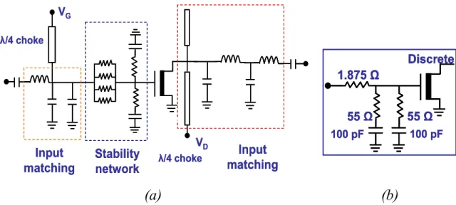
12 Watt Hybrid HPA
Once found the optimum load impedance for the bar, the entire matching networks have to be designed and realized. The prototype hybrid HPA has been implemented by adopting microstrip distributed input/output matching networks and SMD components, in order to synthesize the impedance transformer sketched in the figure below.
Input
matching Stability network
Input matching λ/4 choke λ/4 choke VG VD Input
matching Stability network
Input matching λ/4 choke λ/4 choke VG VD