University of Calabria
Faculty of Science
Chemistry Department - Physics Department
__________________________________________________________________
PhD Thesis
Synthesis and characterization of new
hybrid organic/inorganic materials for
electro-optic applications
Dr.ssa Francesca Teocoli
Supervisor
PhD Coordinator
Prof. Mauro Ghedini
Prof. Carlo Versace
Doctorate in
Science and Technologies of Mesophases and Molecular Materials
(XXIII PhD course) FIS/01, CHIM/03
Courage is the price that life exacts for granting peace. The soul that knows it not, know no release from little things; knows not the livid loneliness of fear, nor mountain heights where bitter joy can hear the sound of wings
Synthesis and characterization of new hybrid
organic/inorganic materials for electro-optic applications
A Thesis
Submitted to the Faculty of Science
of
University of Calabria
by
Dr.ssa Francesca Teocoli
in partial fulfillment of the
requirements for the degree
of
Doctor of Philosophy
December 2010
Contents
Prefac
e 7Chapter 1.
81.1 Hybrid Materials
81.2 Optoelectronic devices
121.2.1 Dye-sensitized solar cells 14
1.2.2 Light-emitting devices 18
Chapter 2. Luminescent mesostructured material
s
212.1 Materials
242.1.1 Mesoporous powder and film 24
2.1.2 Ionic transition-metal complexes 26
2.2 Materials preparation
312.2.1 Co-condensation 33
2.2.2 EISA (Evaporation Induced Self-Assembling) 35
2.2.2.1 Dip-coating 38
2.3 Mesoporous characterization
402.3.1 Photoluminescence properties 43
2.3.1.1Emission spectra, phosphorescence quantum yield
and time-resolved luminescence 44
2.3.2 Powder X-ray diffraction (XRD) 48
2.3.3 N2 sorption 50
2.3.4 Scanning electron microscopy (SEM) 52
2.3.6 Thermogravimetric analysis (TGA) 55
Chapter 3. Solid state dye-sensitized solar cells
563.1 Materials
583.1.1 The substrate 58
3.1.2 The dye 59
3.1.2.1 Z907 63
3.1.2.2 New organic dyes 63
3.1.3 The hole-transport materials 64
3.1.4 The counter electrode 67
3.2 Device preparation
683.2.1 TiO2 layer 68
3.2.2 Sensitizer soaking 71
3.2.3 Hole-transport material deposition 71
3.2.4 Counter electrode deposition and the device sealing 72
3.3 Photovoltaic characterization
743.3.1 Definitions 74
3.3.2 Experimental Data 78
Chapter 4. Lighting devices – (LEEC)
824.1 Device Architecture
834.2 OLEDs vs. LEECs
854.3 Materials
904.3.1 Active layer 91
Chapter 5.
945.1.1 Paper 94
5.1.2 Communications 102
5.2 Solid state dye-sensitized solar cells: results
1045.2.1 Paper 104
5.2.2 Communications 113
Chapter 6. Conclusion and Perspectives
114Acknowledgments
118Preface
The miscellaneous nature of materials science is becoming increasingly prominent, particularly in rapidly growing areas such as nanotechnology. Some of the key words characteristics of this study are Electro- and Photo- chemistry, which play an important role in a vast number of fundamental research and applied sphere of nanotechnology.
Electrochemistry includes, but is not limited to, the exploration of new inorganic and organic compounds, biochemical and biological systems, corrosion, energy applications involving fuel cells and solar cells, and nanoscale investigations.1
Photochemistry pertains to electronically excited molecules which induce reactions.
Therefore photochemistry finds a significant place in varied applications of science and technology. The photophysical phenomena of fluorescence and phosphorescence have found varied functions, for example in light-emitting electrochemical cells (LEEC), photofunctional compounds2, laser technology, and so on.
A further impetus to the study of photochemical reaction has been provided by the energy crisis. This has initiated researches into the conversion and storage of solar energy, processes which plants carry out so efficiently. The fundamental study of excited states of has led to the proper understanding of chemical reactions, modes of energy transfer and the intricate structure of matter.3
At the end, photo-electrochemistry combines photochemical and electrochemical methods for the study of the oxidation-reduction chemistry of the ground or excited states of molecules or ions. In general, it is the chemistry resulting from the interaction of light with electrochemical systems.
Chapter 1
1.1 Hybrid Materials
Since many years, the concept that a mixture of materials can show superior properties compared to their pure counterparts is under scientists and engineers investigation.
Composite materials which are formed by the incorporation of a basic structural material into a second substance, the matrix, are one of the most successful examples of this investigation.
On the other hand, decreasing the size of the structural building blocks which are incorporated into the matrix to the same level as the matrix building blocks could lead to more homogeneous materials that allow a further fine tuning of materials‘ properties on the molecular and nanoscale level, generating novel materials that either show characteristics in between the two original phases or even new properties.
Therefore the term hybrid material is used, in materials science, to identify something that is obtained by mixing components and that the interphase between these components is increased compared to a composite material; in particular, the high homogeneity of the hybrid materials suggests that the two moieties are blended at the nanometer level. 4,5
Otherwise, the hybrid material indicates a class of covalent bonding organic/inorganic components, named class II. In contrast with the class I of composite materials where interactions between organic and inorganic components are provided by hydrogen bonds, Van der Waals forces and ionic bonds, or are electrostatic in nature.
Considering the industrial era, successful commercial hybrid organic–inorganic polymers have been part of manufacturing technology since the 1950s6.
Some of the oldest and most famous organic–inorganic industrial representatives are certainly coming from the paint industries, where inorganic nano-pigments are suspended in organic mixtures (solvents, surfactants, etc.). While the name of ‗‗hybrid‘‘ materials was not evoked at that time, the wide increase of work on organic–inorganic structures was pursued with the development of the polymer industry.
The concept of ‗‗hybrid organic–inorganic‘‘ nanocomposites exploded in the eighties with the expansion of soft inorganic chemistry processes7, and consisted of inorganic and organic building blocks distributed on the molecular or nanoscale.
The modern concept of ―organic-inorganic hybrid materials‖ emerged recently, when the research turned to more sophisticated materials with a higher added value, associated to the development of composites and molecular materials where the organic and inorganic component interact at a molecular level.
As mentioned the first interest in the development of hybrid materials was mainly based on the design of hybrid polymers with special emphasis on structural hybrid materials.
The choice of the polymers is usually guided mainly by their mechanical and thermal behavior. But, other properties such as hydrophobic/hydrophilic balance, chemical stability, bio-compatibility, optical and/or electronic properties and chemical functionalities (i.e. solvation, wettability, templating effect, etc.) have to be considered in the choice of the organic component.
The organic in many cases allows also easy shaping and better processing of the materials. The inorganic components provide mechanical and thermal stability, but also new functionalities that depend on the chemical nature, the structure, the size, and crystallinity of the inorganic phase (silica, transition metal oxides, metallic phosphates, nanoclays, nanometals, and metal chalcogenides). Indeed, the inorganic component can implement or improve electronic, magnetic and redox properties, density, refraction index, etc.7
A variety of silicates or polysiloxanes modified with organic group or networks for the improvement of mechanical properties were the first type of hybrid materials investigated. The expectations for hybrid materials go further than mechanical strength, thermal and chemical stability.
So, in addition to those structural materials and applications, many recent efforts have centered on the design of other types of hybrid materials which explore other fields as electronic hybrids, used in electronics (transistors, diodes), and functional hybrids. Chemical activity is the main characteristic of functional hybrid materials.
The optical and electrical properties, luminescence, ionic conductivity, and selectivity, as well as chemical or biochemical activity, giving way to materials that can be applied for: sensors, selective membranes, all sorts of electrochemical
devices, from actuators to batteries or electrochemical supercapacitors, supported catalysts or photo-electrochemical energy conversion cells, etc.
In these functional materials mechanical properties are secondary (still also important) and the emphasis is on reactivity, reaction rates, reversibility or specificity. The hybrid approach can also be useful in this context by combining organic and inorganic species with complementary properties and reactivities.8,9 Therefore, independently of the types or applications, as well as the nature of the interface between organic and inorganic components, a second important feature in the tailoring of hybrid networks concerns the chemical pathways that are used to design a given hybrid material.
In recent years, the concept of functional nanostructures as hybrid materials has received little attention.
For example, hybrid materials based on block copolymer templating inorganic nanoparticles. The block copolymers are acting not only as nano-reactors to control the size and size distribution of the nanoparticles but also direct the assembly of the nanoparticles into well-defined structures.
Hence, is possible to fabricate a large diversity of functional nanostructures including spheres, rods, and ring-like nano-objects as well as vesicles, whose core can be loaded with different inorganic materials.
The possibility to graft organic functional groups on the walls pore of a porous material allows to product a new class at high performances organic-inorganic hybrid materials10,11.
Three pathways are available for the synthesis of porous hybrid materials based on organosilica units:
i) the subsequent modification of the pore surface of a purely inorganic silica material (―grafting‖),
ii) the simultaneous condensation of corresponding silica and organosilicas
precursors (―co-condensation‖) and
iii) the incorporation of organic groups as bridging components directly and
specifically into the pore walls by the use of bis-silylated single-source organosilica precursors (Periodic Mesoporous Organosilicas (PMO))12.
In this thesis work we will focus on both hybrid systems, the ionic transition metal complexes incorporated into silica porous matrix, and classical organic/inorganic hybrid materials for efficient dye-sensitized solar cells.13
In fact active optical applications of hybrid materials might present a very attractive field. Indeed, the exploitation of active optical properties of photoactive coatings and systems is strongly emerging.
In particular, hybrid materials having excellent laser efficiency and good photostability,14,15 very fast photochromic response,16very high and stable second order non-linear optical response17, or being original pH sensors,18 electroluminescent diodes19 or hybrid liquid crystals20 have been reported in the past years.
1.2 Optoelectronic devices
Nowadays, the optoelectronic system research has been motivated by the potential application of this class of devices in many areas of society. Optical excitation of device leads to useful processes such as light-energy conversion in the form of electricity in solar cells, optical sensors for detection of trace quantities of chemicals, smart windows that on one hand can control the amount of light passing through, or better this class of devices is useful from simple household appliances and multimedia systems to communications, computing, and medical instruments. Design of these devices requires ability to organize molecules on a nanometric scale, with fine control on their arrangement: distribution, mobility, spectral and redox properties.21,22,23,24,25,26,27. Structural organization of these components by controlled molecular engineering allowing synergistic effects is a major feature of these systems.
Optoelectronic devices — from emitting diodes (LEDs), solar cells to light-emitting electrochemical cells (LEECs) — are specifically designed to optimize the light absorption and emission, resulting in high conversion efficiency.
Central to realizing a high-performance and more useful optoelectronic device is the development at the nanoscale that satisfies the trend of a more compact and powerful systems. In the last two decades there have been intense efforts in fabricating organized molecules on a nanometric scale, with a particular attention to the control of their arrangement.
In the photosynthesis of a natural system, figure 1.1, we can find a perfect
example of a device for light-energy conversion.
In the last two decades there have been intense efforts in the fabrication of a similar efficient system because of lacks of knowledge on how to organize molecules on a nanometric scale and to control their reaction efficiencies or improve their structure. The main component, the chromophore, like electron donor and acceptor, is assembled in a high organized structure, and assures a high efficiency photon-to-electron conversion. In artificial systems, we aim for reaching green plant light-energy conversion efficiency, using different sensitizers that absorb light and engage in electron-transfer reaction with suitable electron donors or acceptors. One of the most problematic limitations is the random distribution of these components into the device structure, to achieve the control over the way the components distribute themselves and diffuse towards one another, it is fundamental to confine them in some host supports or matrices.
The term supramolecular is often used to represent such an assembly of several molecules and molecular units.28,29,30,31
In natural systems, the efficiency of light energy conversion is achieved thanks to a highly organized assembly of a chromophore, electron donor and electron acceptor.
Therefore the optoelectronic devices, that involve a photo-sensitizer that absorbs the light and engages in electron-transfer reaction with suitable electron donors or acceptors, have to achieve a controlled spatial distribution, orientation and mutual diffusion of all their components32.
In this thesis work we investigated mesoporous semiconductor surface as the host matrix support.
Major advances in the fields of Sol–Gel chemistry in the last two decades
33,34,35,36,37,38,39
now allow controlled fabrication of micro-, meso- and nano-sized structures.40
Mesoporous materials offer pores that can be filled with a sensitizer and satisfy optoelectronic device paradigm with a high contact between the chromophore and the charged contact of the electric cell.
1.2.1 Dye-sensitized solar cells.
Global environmental concerns and the finite nature of fossil fuels have led to increased interest in the development of renewable energy, and solar energy has emerged as one of the best candidates in this respect. Though conventional photovoltaic devices such as silicon-based solar cells, are promising for the direct conversion of photons into electrons, the prohibitive cost of these cells is uncompetitive with conventional power-generating methods.41 Providing a cost effective and affordable solar energy conversion technology is still a challenge nowadays.42
In a classical p-n junction solar cell a narrow bandgap semiconductor takes over the function of the light absorber and the charge transport material. Figure 1.2
Interband excitation by absorption of a photon of > Ebandgap promotes permits to
an electron to pass from the valence band to the conduction band, leaving a hole in the valence band.
A migration occurs inside or close to the depletion layer of the p-n junction because of the presence of the internal built-in field that split the electron-hole pair and the two charges migrate in opposing direction towards the collecting electrode. Also impurities and microscopic defects can act as recombination centres, decreasing the device efficiency; thereby silicon solar cells are expensive due to
their high-energy consuming production methods that require extremely pure starting materials in addition to sophisticated technical procedures.43
Because of these physical limitations a lot of effort has been invested into the search for new materials. Consequently interest in the prospect of producing cheap alternatives to silicon types is still on the rise. In 1839 Becquerell44 observed for the first time a photovoltaic effect on an illuminated silver electrode, immersed in an iodine/iodide electrolyte. In the 1873 the first sensitized semiconductor was studied by Vogel for application in photography. About 15 years later Moser45 applied this study to a silver plate sensitized with an erythrosine dye, observing an enhancement of photoelectric effect. But a systematic study of dye-sensitization mechanism was developed by Tributsch and Gerischer in 1968.
Gerischer early studies were fundamental to understand electron-transfer processes for a semiconductor in a redox electrolyte; the step forward was in combining the performance of a porous matrix with the dye properties, increasing the amount of absorbed dye in the semiconductor bulk. The concept of dye-sensitized solar cells, introduced by O‘Regan and Grätzel in 1991, was the first promising candidate as an alternative to conventional solar cells.46
The real achievement of Grätzel and his group was to create a 3 orders of magnitude larger TiO2 layer than a normal semiconductor device, consequently a
more efficient device.
The molecular engineering of organic sensitizer leads to a drastic improvement in charge injection efficiency by the synthetization of new class of organic dye with an anchoring group. Recently, thanks to these innovations, the performance of dye-sensitized solar cells based on organic dyes has been remarkably improved and achieved impressive efficiencies in the range of 8 ~ 9.7%.47, 48, 49, 50, 51, 52, 53,54
Dye-sensitized solar cells (DSSCs) are a non-conventional photovoltaic technology that has attracted significant attention because of their high conversion efficiencies and low cost.55 A typical DSSC contains five components: 1) a conductive mechanical support, 2) a semiconductor film, 3) a sensitizer, 4) an electrolyte, and 5) a counter electrode. The total efficiency of the dye-sensitized solar cell depends on the optimization and compatibility of each of these constituents.
Therefore nowadays the new materials like organic molecules and polymers offer several advantages compared to inorganic ones. The properties of a tailored system and the inherent features of organic materials lead to an amazing potential in tuning physical properties such as band gap, valance and conduction energies, charge transport, solubility, morphological properties.
Furthermore organic materials present an easy large scale production and as a consequence economic advantages compared to inorganic materials. Ease of production, due to the small quantities needed for device preparation and the purification, organic materials have furthermore an economic advantage compared to inorganic material.
Basic difference between the conventional solar cells and the dye-sensitized ones, are:
- Dye-sensitized solar cells separate the two functions provided by silicon in a traditional cell design. Normally the silicon acts as both the source of photoelectrons, as well as providing the electric field to separate the charges and create a current. In the dye-sensitized solar cell, the bulk of the semiconductor is used exclusively for charge transport, the photoelectrons are provided from a separate photosensitive dye. Charge separation occurs at the surfaces between the dye, semiconductor and electrolyte.
- Light adsorption and charge carrier transport are separated in dye-sensitized solar cell, whereas both processes are established by the semiconductor in the conventional cell.
The basic functional principle of a dye-sensitized solid-state heterojunction is shown in Figure 1.3.
After the absorption of a photon the excited dye molecule inject an electron in the conduction band of TiO2. The electron, by a percolation process, is diffused
through the porous TiO2 matrix into the current collector like the conducting glass.
During this process the oxidized dye is regenerated by an organic solvent containing a redox system that acts as an electron donor. The cycle is closed when the counter electrode then regenerates the electron donor.
The choice of the electron donor is kinetically crucial in order to avoid a recombination of the oxidized dye with the just injected electron.
The characteristics of the electrolyte must also accommodate the wide range of temperatures to which the cell is exposed in normal outdoor service.
Under long storage or exposure to open air, solvent exudation is unavoidable, leading to low conversion efficiency.56
Thereby the study of the photoinduced charges dynamics is fundamental. The following energetic scheme is a time frames of the reaction for the interfacial electron transfer processes after charge injection from the electronic excited state S* of a dye-sensitizer to the conduction band (cb) of a semiconductor (SC).57
Eqn. (1) Photoexcitation:
Eqn. (2) Charge injection:
Eqn. (3) Dye regeneretion:
Eqn. (4-5) Charge recombination:
1.2.2 Light-emitting devices
Over the past two decades impressive advances have been achieved in the field of light-emitting devices, which are being developed for display and lighting applications.
Light emitting diodes, commonly named LED, are the reverse of photovoltaic cells58. Figure 1.5.
While in this last the light is used to produce an electrical voltage, in a LED a voltage is applied to produce light59. Basically, the electroluminescence occurs when a sufficiently large forward-bias voltage is applied across a p-n junction, where minority carrier injection takes place and radiative recombination produces a photon60.
When a p-type semiconductor is kept in contact with an n-type, electrons move from the n- to the p-doped layer. At the thermodynamical equilibrium the energy levels of the semiconductors are bent and two regions depleted of majority carriers are formed in both sides of the interface.
In this situation, the p-semiconductor is depleted of holes, the n-semiconductor is depleted of electrons and a potential barrier is formed, which hinders the current flow though the interface. If this junction is forward biased, the potential barrier is lowered and the injected electrons in p-type side recombine with the holes and the injected holes in the n-type side recombine with the electrons61. This current flow usually gives rise to an excitation, which results in a radiative recombination process62.
All theoretical considerations about LED involve inorganic semiconductors because of the pioneering works on light emission from GaAs p-n junctions.63,64,65
Figure 1.5. Example of two different optoelectronic device operating modes.
Polymer-based light emitting diodes135, commonly called ―polymer, PLED‖ or ―organic LED, OLED‖, were studied in 1963, but the first work, was only published in 1990.
The light emission process in such devices depends on several parameters, such as charge injection, charge carriers mobility, electron-hole recombination with radiative decay and emission. Charge injection is assigned to the efficiency that the metallic electrodes inject carriers into the polymer film and depends on the Fermi level of the metals. Thus, a hole-injector metal must have high work function, such as: Au or ITO electrodes, and an electron injector metal must possess low work function, such as alkaline or alkaline earth metals.
Polymer based LED present a series of interesting applications, when compared to inorganic materials. The aim of using organic materials as electroluminescent component in a LED, despite their poor light emission properties, results from the difficulty of assembling large areas devices with inorganic semiconductors. Additionally, the mechanical properties of conducting polymers open the possibility of constructing flat panel displays.
Devices fabricated with these materials generally require a multilayer structure and cathodes made of low work function metals in order to achieve high efficiencies and low operating voltages. Recently, the efficiency of small molecule devices has been further increased by employing phosphorescent dyes in the electroluminescent layer since phosphorescent molecules emit from their triplet state.66,67
That notwithstanding, the limited operating life of organic light-emitting devices (OLEDs) is an important factor preventing their wide-scale commercial use in various display applications.
In the mid-1990s Pei and co-workers showed that the properties of organic light-emitting diodes (OLEDs) could be completely transformed by including high concentration of mobile ions in the emissive layer.68,69,70
The light-emitting electrochemical cell (LEEC) is an exciting device concept with potential for various light-emitting applications, such as in thin-film displays,71 solid-state lighting,72 and injection lasers,73 since its successful operation has been demonstrated to be remarkably insensitive to electrode material selection and
active-material thickness, and since impressive power efficiencies have been reported.74
LECs generally require only a single emissive layer, which consists both electronic and ionic conductors sandwiched between two electrodes; mobile ions contained in the solution drift toward electrodes under a sufficient applied bias, cations and anions induce doping (oxidation and reduction) of the emissive material close to the electrodes, that is, p-type near the anode and n-type near the cathode, respectively.
75
The doped regions induce ohmic contacts with the electrodes and consequently facilitate the injection of both holes and electrons, which recombine at the junction between p- and n-type regions. As a result, a single-layered LEC devicehave low electrical resistance and form ohmic contacts with the metal electrodes, consequently can be operated at very low voltages with balanced carrier injection, giving high power efficiencies. Furthermore, air-stable metals, for example, Au and Ag, can be used since carrier injection in LECs is relatively insensitive to work functions of electrodes.76
One limitation in LEC performance comes from the low ionic conductivity of polymeric electrolytes and the phase segregation occurring during LEC operation between the electroluminescent polymer and the solid electrolyte. To improve the ionic conductivity of the blend, Heeger and co-workers included a bifunctional liquid additive to the electroluminescent layer77.
Figure 1.6. Light-emitting electrochemical cells (LECs) based on ionic transition-metal complexes are among the simplest electroluminescent devices as they use only one active component in a mono-or bi-layer architecture, operate with air-stable electrodes and are prepared using solution-basedtechnologies.
Chapter 2
Luminescent mesostructured materials
Early-1990s was particularly rich period for nanotechnologies, with particular relevance to the new materials synthesis, in addition to the preliminary LEEC investigations, by Pei and co-workers, and the first studies on dye-sensitized solar cell, by O‘Regan and Graetzel, the discovery of surfactant-organized silicas and silicates assured attractive applications as catalyst supports, optical materials, sensors, membranes, and selective adsorbents.
As mentioned previously, hybrid materials are a mix of organic and inorganic components at the molecular scale.
Mesoporous materials result from the combination of an organic template acting as a structure-directing agent with an inorganic precursor. They are obtained from hybrid materials by removing the surfactant template. Figure 2.1
The liquid-crystal templating mechanism was used during this thesis work, to fabricate mesostructured materials, in which the condensation of the silica precursor is not the dominant factor for the formation of the mesoporous structure78. The amphiphilic molecules organize themselves in liquidcrystal phases independently of the inorganic crystallization, and the polymerization of the silica precursor takes place around the self-assembled aggregate acting as a template79. Figure 2.1. Pathways for the formation of a mesoporous hybrid material. [Hoffmann et
The LCT is the dominant mechanism when the surfactant concentration is so high that the liquid crystals are already formed when the inorganic precursor starts organizing itself around them80.
Ordered mesostructured powders are generally functionalized with a dye through two different methods: co-condensation (one-pot method) of an appropriate inorganic source and the surfactant self-assembling species doped with an optically active compound, or grafting post-synthesis, due to the presence of a high density of silanol groups on the pore surface of mesoporous material to which guest species may be attached81.
Among the wide variety of films synthesis, thin mesoporous films were produced by evaporation-induced self-assembly (EISA)82 method.83 The coating solution was prepared by the sol-gel method, this process allows the preparation of highly organized and porous layers.
The removal of the organic template is usually performed by calcination or solvent extraction. The first way is cheaper, but can lead to structural problems depending on the inorganic precursor used and on the eventual presence of functional groups, if functional organic groups are present, then the calcination becomes very risky to perform because the organic group could be destroyed by the high temperatures. Silica is a very good precursor, being resistant and stable enough to maintain its amorphous structure at the temperatures of calcination (500 – 600°C). Many other precursors could crystallize at these temperatures, and this would create several defects in the material because of the strong curvature of the pores, being best compatible with amorphous wall structures84.
In the solvent extraction, the material is functionalized after the removal of the template, that is, by grafting the organic groups into the channels walls during a post-synthesis process.
There are different possible ways to classify porous materials. One is related to the definition of pore size furnished by the International Union of Pure and Applied Chemistry (IUPAC)85. According to the IUPAC, porous materials can be divided into:
- microporous materials, if their pore size is below 2 nm,
Figure 2.2 Mesostructured hybrid materials, containing inside the cavities a
luminescent neutral cyclometallated Iridium(III) complex, using a one-pot method.
- macroporous materials, if their pore size is bigger than 50 nm.
Porous materials can also be classified according to their degree of order: fully crystalline (zeolites); ordered on a mesoscopic length scale, but amorphous on the atomic length scale (surfactant-templated materials); or fully disordered (silica gels)7.
Some mesoporous materials are also mesostructured, because a monosized pore is coupled with long range ordered voids. Mesostructures depend by chemical and processing parameters, therefore a great number of characteristics can be tuned, as well large active surface area, pore dimension, and pore shape86. In general mesostructured materials are defined as mesoporous materials before calcination or chemical extraction.
Mesostructured materials are highly versatile substrates for the formation of functional materials, in particular silica at first and then titania mesoporous materials have led to many promising applications in areas ranging from photovoltaics and photocatalysis to photo-electrochromics and sensors. Many of these applications depend not only on the properties of the TiO2 or SiO2 material
itself but also on the modifications of the object host, e.g., with inorganic and organic dyes.
Photo-electronically functional molecules can form specific arrangements in mesopore nanospace, possibly leading to novel functions, which cannot be obtained in open space.
2.1 Materials
2.1.1 Mesoporous powder and film
Ordered mesoporous silicates have attracted a great deal of interest in the past decade because of their use in catalysis, separations, sensors, drug delivery, and optical devices. Mesoporous silica nanoparticles were first synthesized in 1992, through a hydrothermal sol-gel synthesis87, by researchers working for the Mobil Corporation. They had a uniform hexagonal array of pores which had sizes between 20 and 100 Angstrom.88 This material was named Mobil Crystalline of Materials, or MCM-41.89 Discovery of the M41S family of materials ended the long-standing pore-size constraint of zeolites.10,90
Six years later, researchers at the University of California in Santa Barbara announced that they had produced silica nanoparticles with much larger 20 - 300 Angstrom pores91. The material was named Santa Barbara Amorphous type material, or SBA-15. These particles also have a hexagonal array of pores. At the first these types of particles was used as molecular sieves.
Like zeolites, mesoporous materials are characterized by very large specific surface areas, ordered pore systems, and well-defined pore radius distributions. To enable practical applications of mesoporous materials, synthesis strategies have been developed to form thin films. 92
The sol-gel synthesis is a versatile solution process initially used for the preparation of inorganic materials such as glasses and ceramics of high purity and homogeneity.93 It involves the transition of a system from a liquid ―sol‖ into a solid ―gel‖ phase and has been the subject of several books and reviews.10,94
The sol-gel process can ordinarily be divided into the following steps: forming a solution, gelation, aging, drying, and densification. In the preparation of a silica film, one starts with an appropriate alkoxide, tetraethyl orthosilicate (TEOS), which is mixed with water and a mutual solvent, such as ethanol, to form a solution, hydrolysis leads to the formation of silanol groups Si-OH. These species are only intermediates as they react further, i.e. condense, to form siloxane Si-O-Si groups. As the hydrolysis and condensation reactions continue, viscosity increases until the ―sol‖ ceases to flow and form the ―gel‖. There are several parameters which influence the hydrolysis and condensation reactions (sol-gel process), including the activity of metal alkoxide, water/alkoxide ratio, solution pH, temperature, and nature of the solvent and additive.
In this study, mesoporous silica powders are synthesized by reacting Tetraethyl orthosilicate using two different surfactants. Figure 2.3. The selected surfactants are the cationic Cetyltrimethyl ammonium bromide (CTAB, 99.8 wt%), purchased from Alfa Aesar, formed by amphiphilicmolecules with a polar head group and an hydrophobic chain.
The non-ionic triblock copolymer poly(ethylene glycol)-block-poly(propylene glycol)-block-poly(ethylene glycol) (P123), purchased from Sigma-Aldrich. In one molecule ethylene oxide (EO)n monomer blocks are separated by a block of
propylene oxide (PO)n. The hydrophobic core of the micelles formed from such
polymers is composed of hydrophobic PO part, while hydrophilic EO blocks are pointing outwards.
The result is an inorganic scaffold with a regular arrangement of pores. The template can then be removed by washing with a solvent like ethanol95.
MCM-41 sample, obtained with CTABr surfactant, consists of amorphous silica and shows the hexagonal symmetry of the pore ordering (space group: p6m). The pores can be tailored to diameters between dp = 1.5 and 20 nm, largest pores can
only be obtained with the addition of swelling agents. The pore walls are quite thin with a thickness between 1 and 1.5 nm. The presence of these thin pore walls leads to low chemical and hydrothermal stabilities96,97
SBA-15 sample was obtained with Pluronic P123 surfactant, is a combined micro- and mesoporous material with hexagonally ordered tunable uniform mesopores (4– 14 nm)98,99. It consists of thick microporous silica pore walls responsible for the high hydrothermal stability of SBA-15 compared to other mesoporous materials with thin pore walls like MCM-41.
Both the materials show hexagonally arranged channels, large surface area [< 1000m2/g] and a characteristic long range ordered framework with uniform mesopores. Figure 2.4.
Figure 2.3 Chemical formula and shape of Pluronic 123 (left) and CTABr (right)
I
n 1999, Brinker et al.100 reported a new approach, which resulted in highly ordered mesostructured thin films, called ‗‗Evaporation Induced Self Assembly‘‘ (EISA). One of the most important advantages of this synthesis route is the short mesophase formation (a few minutes).
Hybrid mesostructured silica films were prepared adding a surfactant, Pluronic F127 (EO106-PO70-EO106), to a solution of tetraethoxysilane (TEOS), ethanol (EtOH), water, and chloridric acid (HCl). Then a spatially-patterned101 silica thin-film mesophases is formed thanks to the preferential evaporation of alcohol that accompanies the dip-coating deposition.102,103,104,105,106
2.1.2 Ionic transition-metal complexes
For a long time people thought that the luminescent dyes used since the work of Tang et al. are theoretically limited to an internal conversion efficiency of 25% 107. This factor arrives from quantum mechanics, where 75% of the charge wave functions are of the non-emissive triplet case and only 25% of the singlet case, allowing radiative recombination. Taken into account that only one-fifth of the created photons can leave the device, the external quantum efficiency was limited to 5% 108. But, in contrast to this, the family of the so-called phosphorescent dyes (triplet emitters) permits the opening of an additional radiative recombination channel and harvesting of up to nearly 100% of the excited states to photon creation. Responsible for this is the presence of heavy metal atoms such as Ir109 , leading to a strong spin-orbit coupling110.
Iridium(III) cyclometalated complexes are attracting widespread interest because of their unique photophysical properties and applications in organic light-emitting
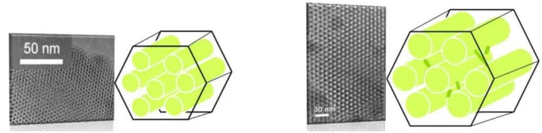
Figure 2.4. MCM-41 and SBA-15 materials with characteristic morphologies.
diodes (OLEDs). Neutral Ir cyclometalated complexes in OLEDs showed up to 19% external quantum efficiencies 111,112,113,114.
As mentioned in the previous chapter, an alternative to the OLEDs, which require a complicated multilayered structure for charge injection, transport, and light emission, is the light-emitting electrochemical cell (LEC) 115,116,117,118,119, in which the use of ionic complexes facilitates electronic charge injection into the light-emitting film32,120,121.
OLEDs and LECs require a tunable phosphorescence wavelength emitter with a very high phosphorescent quantum yields.
A strategy to tune the emission color in Ir(III) complexes relies on the selective HOMO stabilization and/or LUMO destabilization of the complex. Mixed ligand Ir complexes with C^N cyclometalating ligands, are particularly appealing in this respect, since the two types of ligands can be almost independently functionalized to obtain the desired color tuning 122.
In particular, electron-withdrawing substituents on the C^N ligands decrease the donation to the metal and therefore stabilize the metal-based HOMO.
Electron-releasing substituents on the C^N ligand, lead, on the other hand, to destabilization of the ligand-based LUMO, ultimately leading to increased HOMO–LUMO gaps and emission energies.
On the other hand, the control of the factors that act in order to increase the emission quantum yields in mixed ligand complexes, is a daunting task. It is indeed generally assumed that emission quantum yields should increase with increasing emission energy, due to the increase of the radiative rate constant and decrease of the non-radiative rate constants. These follow, respectively, the Einstein law of spontaneous emission123 and the so-called energy gap law 124, even though exceptions to these rules are quite common.
Photophysical Properties
The photophysics of polypyridyl complexes of Ir can be understood with the aid of an energy level diagram, as shown in Figure 2.5.
In these complexes there are three possible types of excited states: (a) metal-centered (MC) excited states, which are due to promotion of an electron from t2g to
without spin change is allowed, which is called singlet–singlet absorption. The allowed transitions are identified by large extinction coefficients. The transitions
with spin change are called singlet–triplet absorption, which are forbidden and associated with small extinction coefficients.
However, the excited singlet state may be involved in spin flip, which is called intersystem crossing (ISC), resulting in an excited triplet state. The radiative process of a singlet and triplet excited state to a singlet ground state is termed fluorescence and phosphorescence, respectively. The excited singlet states associated with LC π–π and MLCT transition can undergo ISC into the triplet state efficiently in Ir complexes due to spin-orbit coupling, resulting in enhanced phosphorescence quantum yields.
For the cyclometalated Ir complexes, the wave function of the excited triplet state, responsible for phosphorescence, is principally expressed as a combination of the LC and the MLCT excited triplet state. However, not all the complexes are highly luminescent because of the different deactivation pathways27.
Tuning of Phosphorescence Colors in Neutral Iridium Complexes
Neutral Ir complexes were obtained by an orthometalation reaction with ligands that contain a benzene ring attached to a functional group containing a donor atom such as 2-phenylpyridine (ppy)125. The coordination of ppy ligands to metal is analogous to that found in 2,2‘-bipyridine except that nitrogen is replaced by
Figure 2. Schematic and simplified molecular orbital diagram for an octahedral d6 metal
complex involving 2-phenylpyridine (C3 symmetry)-type ligands in which various possible transitions are indicated.
carbon anion126. In a typical example, three ppy ligands coordinate around Ir(III) resulting in a neutral complex, in which the phenyl group carries a formal negative charge due to loss of proton and subsequent orthometalation to Ir metal. The HOMO in tris-phenylpyridine Ir(III) [Ir(ppy)3] is principally composed of orbitals
of the phenyl ring and the metal d orbitals. The pyridine is formally neutral and is the major contributor to the LUMO in the [Ir(ppy)3] complex127.
The absorption spectra of [Ir(ppy)3] display strong ligand-to-ligand (LC, π–π) and MLCT transitions in the UV and the visible region, respectively.
The MLCT transition bands are lower in energy than the LC π–π transitions. The excited triplet state shows strong phosphorescence in the green region at around 515 nm, with an excited state lifetime of 2 s128.
In order to tune the phosphorescence color of [Ir(ppy)3], Watts et al. synthesized
several substituted ppy-based neutral Ir complexes45,129,130. The phosphorescence lifetime of these complexes is in the range of 2–3 s in nitrogen-saturated acetonitrile at room temperature46.
Controlling Quantum Yields in Iridium Complexes
Orthometalated Ir complexes are known to have highest triplet emission quantum yields due to several factors131,132:
• Ir has a large d-orbital splitting compared to other metals in the group.
• Strong ligand field strength of the ppy anionic ligand increases the d-orbital splitting, leading to an enlarged gap between the eg orbitals of Ir and the LUMO of
the ligand.
• Close-lying π–π and MLCT transitions, together with the heavy atom effect, enhance the spin-orbit coupling.
However, the mixed ligand cationic Ir complexes show appreciably lower quantum yields compared to the tris-orthometalated Ir complexes because of the lower LUMO orbitals of the 2,2‘-bipyridine ligand 32,45,133. One strategy to increase the quantum yields of Ir complexes is to introduce F and/or CF3 substituents. This
results in a stabilization of both the HOMO and the LUMO. Since the HOMO stabilization is larger than that of the LUMO, this leads to an increase in the gap between HOMO–LUMO134.
N Ir
N N
Figure 2.6. Chemical structure of fac-isomer of the neutral
homoleptic tris-cyclometalated 2-phenylpyridine Iridium(III) complex, fac-Ir(ppy)3 where Hppy=
2-phenylpyridine.
Application
Introducing dye molecules, with appropriate energy levels for color tuning, in the emitting layer of a light-emitting device, is an established way to improve the optoelectronic device performance.
Besides this aspect, doping also leads to a change of the transport characteristics and to a considerable increase of the lifetime and of the quantum efficiency.
The common way of device realization is to a mix small concentration of a highly phosphorescent guest into a host material with suitable charge transport abilities. Taking into account an unchanged out-coupling factor of one-fifth, the theoretical external quantum efficiency for the triplet dyes jumps up to 20%135.
As stated above, photochemical, photophysical and electrochemical properties of Ir(III) cyclometalated phenylpyridine (ppy) compounds, has been intensively investigated because of their potential application as light-emitting device and solar cells27.
Luminescent iridium(III) complexes are highly appealing due to their wider range of emission energies, longer lifetimes, higher luminescence quantum yields, and for their properties of being liquid crystal systems.
However, it is also noteworthy that the actual performances of these molecular materials can be often severely limited because of the reduced emission efficiency in the solid state, owing to a concentration-driven quenching.136
Although different approaches, such as the dispersion of the emitters in a polymeric matrix or the introduction of sterically hindered substituents into the auxiliary ligands137,138 have been explored to limit the concentration quenching effect, at present none of them seem to sufficiently solve this problem. In this context, mesostructured materials can be a useful way for the emitting Iridium(III) complexes dispersion, thus obtaining best performing Iridium(III)-based
Figure 2.8. Periodic mesoporous organosilicas (PMOs).
Image copyright:
http://www.uni-giessen.de/cms/fbz/fb08/chemie/iaac/froeba /research/pmo
luminescent materials. In fact, an homoleptic tris-cyclometalated Iridium(III) surfactant has been recently employed in the synthesis of an amphiphile/silica co-assembled nanocomposite which was successfully used as active layer for organic light-emitting diode. This provided a better performing device with respect to the one based on the pristine solid.139
2.2 Materials preparation
The incorporation of functionalities, such as luminescent Iridium(III) complex, can generally be achieved in three ways. Grafting is a post-synthesis treatment of a mesoporous material by which a subsequent attachment of functional molecules onto a mesoporous silica matrix takes place. Figure 2.7.
Through incorporation of condensable organosilane inside the pore wall of the porous mesophase that lead to periodic mesoporous organosilicas (PMOs)140, unlike in organic functionalized mesoporous silica phases obtained via grafting or co-condensation procedures the organic groups in PMOs are direct parts of the 3D framework structure, Figure 2.8.
Figure 2.7. Grafting (post-synthetic functionalization) for organic modification of
mesoporous pure silica phases with terminal organosilanes of type (R‘O)3SiR. R‘=organic
functional group.
The co-condensation technique is a simultaneous reaction of condensable inorganic silica species and silylated organic compounds (co-condensation is equal to one-pot synthesis), the co-condensation synthesis often caused the loss of ordering structure of mesoporous silica.
During this Thesis work we have investigated two methods, the impregnation technique, a post-synthesis method similar to a grafting, which consists in the soaking of mesoporous material into a dye solution, and a one-pot-like method, in which new materials are formed by the co-condensation of a luminescent complex, with the inorganic silica precursor in the presence of template. Co-condensation properties are simultaneous functionalization and structure formation, homogeneous distribution of dyes into the porous matrix and controlled final stoichiometry similar to original solution composition. Figure left.
The new materials described and discussed herein are obtained by a one-step procedure, similar to that developed by Zhou et al.141, co-assembling the neutral luminescent Iridium complex with a surfactant, which acts as structure-directing agent, and tetraethoxysilane (TEOS) as inorganic source. Moreover, because of the negligible solubility of Iridium(III) complex in H2O, EtOH has been used as
co-solvent in order to increase, at least slightly, the Iridium(III) complex solubility and make easier its inclusion within the hydrophobic regions of the surfactant during the template self-assembly process.
The silica-based luminescent materials prepared according to the above summarized procedure, with the general formula SiO2([Ir]•CTAB) and
SiO2([Ir]•P123), have been structurally and photophysically investigated.
The differences induced by i) the nature of the reacted surfactant with respect to the neutral character of Iridium(III) complex ii) the resulting structural differences induced by the use of ethanol as co-solvent in the synthetic procedure and iii) the resulting structural differences induced by the introduction of the Iridium(III) complex luminescent complex will be discussed.
2.2.1 Co-condensation
The new ordered mesostructured materials, as mentioned above, were prepared by co-condensation of an appropriate inorganic source and the surfactant self-assembling species doped with an optically active compound, in particular the chromophore is added to the reaction mixture, which was stirred at room temperature for 5 h, then the SiO2 precursor, TEOS, is added.
Mesostructured materials with a geometrically regular inorganic skeleton have been shown to be appropriate scaffolds for the confinement of dyes.142,143,144,145 The goal was to incorporate a highly luminescent species in a mesoporous material preserving, at the same time, the ordered porosity and the high surface area of the matrix.
Materials
Tetraethyl orthosilicate (TEOS, 98%), ammonium hydroxide (NH4OH, 29 wt%
NH3 in water), poly(ethylene poly(propylene
glycol)-block-poly(ethylene glycol) (P123), hydrochloric acid (HCl 37%), and absolute ethanol (EtOH, 99.98%) were used as supplied by Sigma-Aldrich. Cetyltrimethyl ammonium bromide (CTAB, 99.8 wt%) was purchased from Alfa Aesar. Water was produced from a Milli-Q system. fac-Ir(ppy)3, [Ir], was synthesized according
to the procedure reported in the literature.146
Synthesis
Preparation of mesostructured blank SiO2(CTAB)
SiO2(CTAB) was prepared using a procedure similar to the one described in the
literature.147 Molar composition: 1 TEOS: 0.3 CTAB: 3.8 NH4OH: 153 H2O: 17.1
EtOH. The template solution was prepared by dissolving 1.09 g (0.003 mol) of CTAB in 10ml (0.171 mol) of EtOH under magnetic stirring. Then, 27.5ml (1.53 mol) of H2O and 2.49ml (0.038 mol) of NH4OH were added to this solution. After
5 min, 2.21ml (0.01 mol) of TEOS was added under rapid stirring. The mixture was stirred for 3 days at room temperature, then filtered, washed with H2O and
Preparation of mesostructured blank SiO2(P123)
SiO2(P123) was prepared adapting the procedure described in the literature.148
Molar composition: 1 TEOS: 0.0174 P123: 6 HCl: 167 H2O: 17.1 EtOH. 1 g
(1.74·10-5 mol) of P123 was dissolved in 10ml (0.171 mol) of EtOH, under vigorous stirring at room temperature. Then, 30ml (1.67 mol) of H2O and 1.83ml
(0.060 mol) of HCl were added to the solution. Finally, 2.21ml (0.01 mol) of TEOS were added under stirring. The resulting mixture was aged at 373K for 24h, then filtered, washed with H2O and dried at 333K for 12h.
Preparation of mesostructured hybrid, SiO2([Ir]•CTAB)
Molar ratio: 1 TEOS: 0.3 CTAB: 3.8 NH4OH: 153 H2O: 17.1 EtOH: 0.0016
Iridium(III) complex. CTAB (1.09 g, 0.003 mol) was dissolved in 10ml (0.171 mol) of EtOH; Iridium(III) complex (0.01 g, 1.6·10-5 mol) was added to the reaction mixture, which was stirred at room temperature for 5 h. The obtained yellow suspension was filtered to remove the solid. Then 27.5ml (1.53 mol) of H2O and 2.49ml (0.038 mol) of NH4OH were added to the resulting solution. After
5 min, 2.21ml (0.01 mol) of TEOS were added under vigorous stirring. The mixture was stirred for 3 days at room temperature, then filtered, washed with H2O
and dried at 343 K overnight.
Preparation of SiO2([Ir]•P123)
Molar composition: 1 TEOS: 0.0174 P123: 6 HCl: 167 H2O: 17.1 EtOH: 0.0016
[Ir]. An ethanolic solution (10ml, 0.171 mol) of P123 (1 g, 1.74·10-5 mol) was obtained under vigorous stirring. Then, 0.01 g (1.6·10-5 mol) of Iridium(III) complex was added. The resulting mixture was stirred at room temperature for 5 h. Then the solid product was filtered and 30ml (1.67 mol) of H2O and 1.83ml (0.060
mol) of HCl were added to the solution. Finally, 2.21ml (0.01 mol) of TEOS were added with stirring at room temperature. The mixture was aged at 373 K for 24 h, then filtered, washed with H2O and dried at 333K for 12h.
Template extraction
The surfactant removal was performed using a chemical extraction with solvent. In particular, for the materials obtained with CTAB as template directing agent, EtOH (300 ml) and HCl (25 ml) were added to 1 g of the respective solids,
SiO2(CTAB) and SiO2([Ir]•CTAB). The mixtures were subsequently stirred for 6 h
at reflux. The resulted inorganic scaffolds, named SiO2(CTAB)* and
SiO2([Ir]•CTAB)* respectively, were dried at 343 K overnight.
For the other mesostructured materials, SiO2(P123) and SiO2([Ir]•P123), the
removal of the neutral surfactant P123 was made by a chemical extraction using only EtOH (300 ml), which was added to 1 g of solid sample. The resulting mixture was stirred for 6h at reflux. The obtained solids, abbreviated in a similar way to the other extracted materials SiO2(P123)* and SiO2([Ir]·P123)* respectively, were dried at 343 K overnight.
2.2.2 EISA (Evaporation Induced Self-Assembly)
The film formation by EISA is a chemical performance that implies the coordinated interaction of the following phenomena:
1) Sol–gel chemistry (shape, size, hydrophilicity and connectivity of the inorganic or hybrid nano building blocks).
2) Self-assembly between template molecules, to form micelles, between micelles, to form extended liquid crystalline domains, and between micelles and inorganic or hybrid nano building blocks..
3) A ―race towards order‖ in which the processes of gelling and order from phase separation compete.
4) Mass transport, which controls the homogeneity of the processes (and thus the mesostructure) along thickness.
One of the main parameters that govern the entire film-formation process is evaporation.
As soon as a layer of the initial sol is deposited on the substrate, evaporation of volatile components (ethanol, water, and hydrochloric acid) takes place at the air/film interface. The evaporation leads to the fast and progressive (10-30s) enrichment of the film in silica oligomers and template molecules. When the surfactant concentration has reached the equivalent of the critical micelle concentration (cmc) for the system, micelles start to form by hydrophobic segregation of alkyl chains. An organized mesostructure with respect to the physical-chemical properties of the surfactant molecule in the actual medium is eventually formed.
Figure 2.9. Formation of mesostructured thin film by dip-coating. Step 1: presence of
isotropic initial sol in which the condensation is slowed. Step 2: evaporation proceeds and the micelles start to form above cmc. Step 3: evaporation is completed; the film is in equilibrium with environment and the mesostructure is fixed by relative humidity (RH) before inorganic condensation. Step 4: inorganic network is condensed; hybrid mesostructure is stabilized. Lee et al., 2006 Phys.
Fluids 18, 052105
The evolution of an EISA system as a function of time (i.e., the kinetics of the system) leads to plot diagrams containing the main phases of film formation12. Figure 2.9
If the concentration of the inorganic and template species in the initial dilute solutions is low, no liquid crystalline species will be formed; even micelle formation is difficult under these conditions, because the critical micelle concentration (cmc) of the template in the solvent (often a mixture of low weight alcohols and lower water quantities) is relatively high.
When solvent evaporates, template self-assembly properties become evident, and aggregation processes (i.e., micellization) begin to take place.
When higher concentrations are reached, a liquid crystalline phase is formed, due to micelle aggregation. In the ideal case, micelles pile up in ordered structures and the inorganic building blocks locate themselves in the outside (polar) fraction of
the organic liquid crystal formed. A hybrid mesostructure (inorganic skeleton surrounding an organic liquid-crystalline phase) is thus formed. EISA can thus be described by competitive processes related to the kinetics of condensation versus the kinetic of organization, both influenced by the kinetics of diffusion of the volatile species.However, these processes are difficult to control and thus difficult to predict if they occur successively or simultaneously during drying.
In-situ SAXS experiments coupled with interferometry shed light into these complex assembly processes149,150,151,152. In most of the cases, the mesostructure appears after the drying line (i.e., when practically all the solvent is evaporated and the film attains more or less its final thickness).
This multiplicity of mesophases upon mesostructure formation has been observed by insitu X-ray reflectometry experiments on silica/cationic surfactant films grown at the air–water interface153. In the case of nonionic templates, the formation of a short-range order phase (often called a ―wormlike phase‖) precedes the formation of an organized and well-oriented product mesophase. This kind of ―disorder-to-order‖ transition has also been observed in the initial stages of formation of thick films or xerogels154.When a well-defined organization at the mesoscale is desired, the system has to be designed to separate phases and organize completely before the medium becomes rigid enough to ―freeze‖ a disordered phase, or even to ―freeze‖ before any phase separation, leading to a non-mesoporous, or poorly ordered film. In other words, the race towards order must be won155.
If the thermodynamic differences between ordered or disordered mesophase are not significant at ambient temperature156, the order phase can be formed if
1) the nucleation rate for an organized mesophase made upon the self-assembly of micelles and inorganic counterparts (i.e., the Nano Building Blocks of the hybrid mesophase) is high and
2) the medium is compliant enough to permit rearrangement of the nano building blocks.
Some clues of the condensation kinetics can be obtained by applying in-situ spectroscopic techniques, such as ATR-FTIR spectroscopy157, FTIR ellipsometry158, and IR synchrotron radiation.
2.2.2.1 Dip-coating
Mesoporous films are typically synthesized by evaporation-induced self-assembly (EISA), Figure 9, via dip-coating, using inorganic precursors such as alkoxides, organo-alkoxides or chlorides, and organic templating agents such as amphiphilic block copolymers 159,160,161. Mesoporous films show large surface areas up to 1000 m2 g-1, and pore volumes up to 1.3 cm3 g-1162.
The thickness of the film is mainly determined by the rate of evaporation of the solvent and the viscosity of the solution. When the velocity of substrate and the viscosity of liquid aren‘t very high, the thickness of film can be obtained from Landau and Levich equation:
where U is the speed of extraction, η is the viscosity, γLV is the surface tension
liquid-vapor. It is important to observe that for polymeric systems the thickness of film change with U2/3. This equation assumes constant viscosity and Newtonian behavior, without effects of evaporation. Landau and Levich equation is effective for sol prepared in acid catalysis12.
In this thesis work, we introduced a Iridium(III) complex as light emitting guest species into a mesoporous silica film acting as host matrix. The synthesis of the luminescent material has been performed by a co-condensation approach, similar to the one described above for the powders.
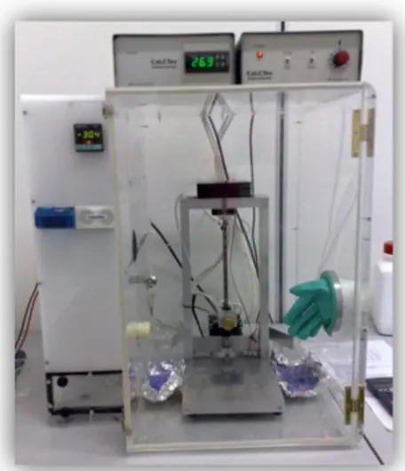
The instrument used was a dip-coater fabricated by workers of University of Calabria spin-off, CalTec s.r.l.(Calabria Liquid Crystals Technology) Figure 2.10.
Figure 2.10. Dip-coater with
temperature and humidity control pannels.
Materials
Pluronic F127 (OH(CH2–CH2O)106(CHCH3–CH2O)70(CH2CH2O)106H), tetraethyl orthosilicate 99% (TEOS), hydrochloric acid (HCl 37%), and absolute ethanol (EtOH, 99.98%) were used as supplied by Sigma-Aldrich. Water was produced from a Milli-Q system. fac-Ir(ppy)3, [Ir], was synthesized according to
the procedure reported in the literature.35 Quartz slides, with area=3cm2, were employed as the substrates. The slides were accurately washed by distilled water, ethanol and acetone before using.
Preparation of silica sol
A first solution, the template solution, was prepared by dissolving 1.3 g of Pluronic F127 and 0.01 g (1.6·10-5 mol) of Iridium(III) complex in 15 ml of EtOH and 1.5 ml of HCl acid aqueous solution (5.7 x 10⁻² M). The resulting mixture was stirred at room temperature for 5 h. A stock solution was prepared by adding (in the following order) ethanol, TEOS, water, and HCl in the molar ratios TEOS:EtOH:H2O:HCl = 1:2.78:1.04:1.43x10⁻². The sol was left to react under
stirring 75 min at room temperature. The final sol was obtained by adding 7.7 ml of the stock sol to the solution containing the block copolymer. The final molar ratios were TEOS:EtOH:H2O:HCl:PluronicF127:[Ir]=1:16.3:5.4:1.88x10⁻²:5x10 -3
:0.0016 [Ir]. The sol was stirred at room temperature for 15 min and immediately used for film deposition.
Preparation of silica films
The films were deposited on the substrates via dip-coating at room temperature. The film depositions were performed at 24% relative humidity (RH), at the withdrawal speed of 15cm min-1. After the deposition, the films were dried at 60°C for 12h. We obtained two kind of materials: a mesostructured SiO2([Ir]•F127) and
a mesostructured blank SiO2(F127), then calcined in air for 60min at 350°C.
2.3 Mesoporous characterization
Low angle X-ray diffraction (XRD) measurements were performed in the 2θ range of 1.0°-10.0° with a Philips 1730/10 diffractometer using Cu Kα radiation (λ = 1.5416 Å) at 40 kV and 200 mA and at-a-step width of 0.005°.
Nitrogen sorption isotherms were measured at 77 K on a Micromeritics ASAP 2010 porosimeter. The materials were outgassed for 12 h under vacuum at 423 K before the measurements.
Specific surface areas were calculated by the Brunauer-Emmett-Teller (BET) method and pore sizes by the Barrett-Joyner-Halenda (BJH) methods.163,164
Scanning electron microscopy images (SEM) were obtained with FEI FP 2353/0X. The thermogravimetric analysis (TGA) was carried out between 298 K and 1093 K under an air flow and at a heating rate of 10 K/min in a Perkin Elmer thermobalance.
Transmission electron microscopy (TEM) images of mesoporous materials were obtained in the bright field mode on a JEOL 200C9 microscope equipped with a tungsten cathode operating at 200 kV. Mesoporous powders were deposited on a
carbon-coated copper grid. Performed in the Laboratory of Materials Science and Nanotechnologies, CR-INSTM, University of Sassari.
Steady-state emission spectra were recorded on a Horiba Jobin Yvon Fluorolog 3 spectrofluorimeter, equipped with a Hamamatsu R-928 photomultiplier tube. The procedure involves in mesoporous materials characterization, are, primarily, X-Ray powder Diffraction (XRD) which should be carried out at wide and low angles. The XRD powder d spacings of well-prepared MCM-41 can be indexed on a hexagonal and cubic lattice, respectively. XRD combined with other techniques, such as HRTEM, electron diffraction, and lattice images, are key methods for the characterization of these materials and identification of the phase obtained, i.e. hexagonal (MCM-41).
Adsorption of molecules has been widely used to map the pore size distribution of mesoporous solids. In this sense, the physisorption of gases such as N2, O2, and Ar
have been used to characterize the porosity of M41S samples and more specifically MCM-41.


![Figure 2.11. Emission spectra of SiO 2 ([Ir]•CTAB) (dash line), SiO 2 ([Ir]•P123) (dot](https://thumb-eu.123doks.com/thumbv2/123dokorg/2880567.10310/46.892.175.759.717.1091/figure-emission-spectra-sio-ctab-dash-line-sio.webp)
