I
Dedication
To my late father, God bless his soul,
To my mother, wish you wellness,
To my lovely wife and kids,
I dedicate this Research.
II
ACKNOWLEDGMENT
Undertaking this PhD has been a truly life-changing experience for me and it would not have been possible to do without the support and guidance that I received from many people.
So, firstly I would like to sincerely thank my supervisor Prof. Lorenzo S. Caputi for his excellent guidance, he knew how to guide my research thanks to his high vision in both scientific and general cultures, I am indebted to him indefinitely.
Also I would like to thank the educational institutions in Sudan; University of Kassala and MOHE for their estimated support.
My thanks extend also to the members of Laboratory of Surface Nanoscience for their friendship and for providing me the best conditions to carry out my research. Particularly, I want to thank Dr. Anna Cupolillo for her valuable guidance, kindness and professionalism in the scientific matters which have allowed me to be more efficient throughout the period of my research. Also I express special thanks to all my seniors and juniors colleagues in the lab; Nadia, Denia, Marlon, Diana, Francesca and Andrea for the good teamwork and lovely friendship environment they have given me.
I am also grateful to my family support. I would like to thank my kind mother for her encouragement, wishes and her continuous prayers to achieve and complete my work. Also I would like to thank my brothers and sisters for their constant support and encouragement. In particular I thank my own family; wife and children for their encouragement and patience throughout the PhD period, I owe to them.
Finally, I would like to express my deep appreciation to all the friends I have known at the UNICAL, in particular to all Sudanese friends for the wonderful moments we have spent together.
III
CONTENTS
Dedication ... I Acknowledgment ... II CONTENTS ... III List of Figures... V ABSTRACT ... XI ABSTRACT (Italian Version) ... XIIICHAPTER ONE
INTRODUCTION ... 1
1.1 Graphene ... 4
1.2 Silicene ... 8
1.3 Carbon nano-onions (CNO) ... 11
CHAPTER TWO EXPERIMENTAL METHODS ... 13
2.1 Ultra-High Vacuum (UHV) Chamber ... 14
2.2 Low Energy Electron Diffraction (LEED) ... 15
2.3 X-ray Photoelectron Spectroscopy (XPS) ... 17
2.4 Electron Energy Loss Spectroscopy (EELS) ... 20
2.4.1 Theoretical Fundaments ... 24
2.4.2 EELS in reflection geometry ... 29
2.5 Raman Spectroscopy ... 30
2.6 Transmission Electron Microscopy (TEM) ... 34
2.6.1 Fundamental Theory of TEM ... 35
CHAPTER THREE GRAPHENE ... 40
Graphene on Ni(111) ... 41
IV
3.2 Atomic Structure of Graphene on Ni(111) ... 43
3.3 Electronic Structure of Graphene on Ni(111) ... 44
3.4 Low Energy Plasmon of Graphene/Ni(111)... 51
3.5 Interface-π Plasmon of Graphene/Ni(111) ... 56
3.6 K-edge ELNES of Graphene/Ni(111) ... 61
3.7 Conclusions ... 65 CHAPTER FOUR SILICENE ... 66 4.1 Silicene on Ag(111) ... 67 4.2 Conclusions ... 81 CHAPTER FIVE CARBON NANO-ONIONS ... 82 5.1 Carbon Nano-Onions... 83 5.2 Synthesis of CNOs ... 87 5.3 Conclusions ... 103 REFERENCES ... 104 PUBLICATIONS ... 121
V
List of Figures
Figure 1.1: Graph shows dramatic growth in published papers related to nanotechnology. ... 2
Figure 1.2: (a) Crystal structure of the graphene layer, where carbon atoms are arranged in a honeycomb lattice. The unit cell of graphene with lattice constant a has two carbon atoms per unit cell, A and B. (b) Electronic dispersion of and states in the honeycomb lattice of free-standing graphene. (c) Band structure of free-standing graphene ( , and bands are marked). ... 4
Figure 1.3: Top-view of a simple ball model for the top-fcc graphene/Ni(111) system is shown. Carbon atoms are small black spheres and nickel atoms are big blue spheres. ... 6
Figure 1.4: Two ways of the graphene preparation on metal surfaces: (a) Segregation of bulk-dissolved carbon atoms to the surface at high temperature Tsegr; (b) Decomposition (cracking) of hydrocarbon molecules at the surface of transition metals at high temperature Tcrack ... 7
Figure 2.1: Ultra High Vacuum Chamber in Nanoscience Laboratory ... 14
Figure 2.2: Picture of low energy electron difraction apparatus. ... 15
Figure 2.3: Diagram of Low Energy Electron Diffraction apparatus. ... 16
Figure 2.4: Ewald's sphere construction for the case of diffraction from a 2D-lattice. ... 17
Figure 2.5: Schematic figure of an XPS system. ... 18
Figure 2.6: Schematic diagram of the XPS process, showing photoionization of an atom by the ejection of a 1s electron ... 19
Figure 2.7: Electrons mean free path as function of their energies. ... 21
Figure 2.8: Energy of the electrons emitted after the interaction with a beam of primary electrons of energy Ep. ... 22
Figure 2.9: Real and imaginary part of the dielectric function ε (upper side) and real and imaginary part of 1/ ε (bottom side) for the Drude model. ... 26
VI Figure 2.10: Real and imaginary part of the dielectric function ε (upper side) and real and
imaginary part of 1/ ε (bottom side) for the Lorentz model. ... 28
Figure 2.11: EELS reflection geometry representation ... 29
Figure 2.12: Raman spectroscopy:(a) laser-sample interaction; (b) Raman effect; (c) Raman spectrum ... 32
Figure 2.13: Raman spectra of graphite (top) and graphene (bottom) [95]. ... 33
Figure 2.14: Evolution of the 2D peak from monolayer graphene to bulk graphite. The 2D peak‟s shape changes with respect to the thickness of the sample [95]. ... 34
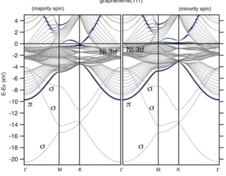
Figure 3.1: Calculated majority and minority spin band structures for a slab terminated by graphene/Ni(111) interface for a most energetically favorable top-fcc configuration. For the blue (darker) lines, the carbon pz character is used as a weighting factor. [107] ... 42
Figure 3.2: (a) A topographic STM image of the high-quality graphene/Ni(111) system. The
inset shows a LEED image obtained at 63 eV. (b) Magnified STM image of the perfect graphene lattice. The graphene honeycomb is marked in (b). Data are taken from [109] ... 43
Figure 3.3: (a) Angle-dependent C 1s NEXAFS spectra of the graphene/Ni(111) system
measured as a function of angle θ, between polarization vector of the incoming linearly polarized light and the surface normal. (b) Comparison between experimental NEXAFS spectra and calculated EELS of graphite and graphene/Ni(111) for two different incident angles, θ , where transitions from C 1s core level on mostly - or -states occurred. Experimental and theoretical data are from [46,59] and [110] respectively. ... 45
Figure 3.4: (a) Time evolution of the PES intensity in the C 1s region during the graphene
growth. Individual spectra were recorded every 10s. F and G mark the signals from C3H6
fragments and graphene, respectively. The inset shows a LEED pattern (primary energy was 80 eV) after growth of graphene. (b) C 1s PES spectra of the resulting graphene layer obtained at different temperatures. Data are taken from [119] ... 47
Figure 3.5: Angle-resolved photoemission spectra of the graphene/Ni(111) system recorded
VII
photon energy. Spectra corresponding to Γ and K points are marked by thick black lines.
[109] ... 48
Figure 3.6: Constant energy cuts of the 3D data sets in the energy-wave vector space, I(EB, kx, ky), obtained through a β-scan from the graphene/Ni(111) system at 100 eV of photon energy. The energy cuts are taken at (a) 4 eV and (b) 2.7 eV BE as well as at (c) EF. [109] ... 50
Figure 3.7: (a) AES spectra of clean Ni surface (bottom curve) and graphene/Ni (111) system; (b) LEED image of the graphene/Ni (111) system collected at a primary electron energy of 65 eV ... 52
Figure 3.8: EEL spectra obtained on graphene-covered Ni (111) for different values of the scattering angle θs. The fitting curve (Gaussian + polynomial background) was superimposed on each experimental curve. The position of the main peak in the spectrum has been used to calculate the indicated q|| value ... 53
Figure 3.9: Energy dispersion relation of the observed loss peak. The solid curve represents the best fit of our experimental result according to full RPA dispersion ... 54
Figure 3.10: EEL spectra obtained on clean Ni(111) (lower curve) and graphene-covered Ni(111) for different experimental geometries. The q|| values calculated for each of the dispersing interface-π plasmon peaks, are shown on the right side. ... 57
Figure 3.11: Energy loss values of the interface-p plasmon peak plotted vs. q||. The line represents the dispersion curve obtained by a square-root fit of the experimental points, whose equation is given in the text. ... 58
Figure 3.12: C KVV AES peak (a) and LEED pattern (b) for graphene on Ni(111). ... 61
Figure 3.13: (a) The RELNES spectrum of the carbon K-edge measured on graphene/Ni(111). (b)–(d) First principle calculations for graphene/Ni(111), graphene, and graphite, respectively. ... 62
Figure 4.1: Ag(111) sample (8mm diameter) mounted on the sample holder ... 74
Figure 4.2: LEED pattern of the clean Ag(111) sample ... 74
VIII Figure 4.4: XPS spectra obtained after silicon deposition (red curve) and for clean Ag(111)
substrate (black curve). ... 75
Figure 4.5: (a) and (b) LEED patterns of silicene on Ag(111) taken at room temperature with the kinetic energy of 40eV. (c), (d), LEED patterns reproduced from Jamgotchian et al. [46]. ... 76
Figure 4.6: (a) Ordered arrangement of silicon atoms on the Ag(111) surface which give rise to
the LEED patterns observed: (a) and (d) . ... 77
Figure 4.7: (a) EEL spectra for the clean Ag(111) measured for different values of the parallel
momentum transfer . (b) Energy dispersion curves of the surface plasmon peak for Ag(111). ... 78
Figure 4.8: EEL spectra of the Ag(111) surface covered by Silicene in the (4×4, √13×√13R19°,
2√3×2√3R30°
) phase (red curve). For comparison, the spectrum of the clean surface is also shown (black curve). ... 79
Figure 4.9: EEL spectra of the Ag(111) surface covered by Silicene in the 2√3×2√3R30° phase, obtained at different detection angles. The values of the momentum transfer relative to the loss at about 0.7 eV are shown. ... 80
Figure 4.10: Dispersion relation obtained from the spectra shown in Figure 4.9 ... 81
Figure 5.1: Scheme of the apparatus used for the arc discharge synthesis of CNOs. [162] ... 83
Figure 5.2: Suggested mechanism for the formation of carbon nano onions produced in water. (a) Direction of the electric field formed between the two electrodes. (b) Direction of thermal expansion from the plasma to water. (c) Ion density distribution as a function the distance from the plasma. (d) Gradient of temperature and formation of different
nanoparticles. [162] ... 84
Figure 5.3: Raman spectrum of a sample containing polyhedral carbon onions. In the inset the corresponding TEM image is displayed. [173]... 86
IX Figure 5.5: Diagram of apparatus for synthesis of CNOs by arc discharge in water. ... 89
Figure 5.6: Digital image of the experimental process during arc discharge between anode and cathode of graphite. ... 90
Figure 5.7: Discoid formed on the cathode during arc discharge. ... 90
Figure 5.8: Material gendered by arc discharge in the synthesis chamber. ... 91
Figure 5.9: Suspensions obtained after sonication of the three groups of material collected in reaction chamber: (a) from surface the reaction water, (b) collected on bottom of
reaction water... 91
Figure 5.10: Agglomerates formed on the cathode, a) heated to 400 °C, b) without heating. .... 92
Figure 5.11: (a) TEM image shows agglomerates of different CNPs (CNT, CNO, lamellar structures). (b)Zoom image shows clearly agglomerates formed only of CNOs and CNTs ... 93
Figure 5.12: TEM image of a carbon-onion of high dimension and inset SEAD image... 93
Figure 5.13: TEM images of (a) planar and corrugated fragments without evidence of CNOs and (b) clear corrugate structure of high dimension with low presence of CNOs. ... 94
Figure 5.14: TEM images of carbon nanomaterials observed in Bp sample. ... 95
Figure 5.15: (a) image conteneting only CNOs of extended diameter observed in Bp sample. (b) CNO of extended diameter and sorrundimg of smaller CNOs. ... 95
Figure 5.16: SEM images of CNTs produced during synthesis of CNOs by arc discharge in water. (a) Sp sample and (b) Bp sample. ... 96
Figure 5.17: Raman spectra of graphite (a) and floating CNPs formed on surface (b). ... 96
Figure 5.18: a) TEM image shows agglomerates of different CNPs (with more amounts of CNOs). b) Image shows clearly agglomerates formed only of CNOs. ... 97
Figure 5.19: TEM images of grinded Ds sample. (a) Fragment consisting of only CNOs clearly distinguishes each one. (b) Image shows clearly polyhedral structures of CNOs, (c) A polyhedral CNOs with dimensions of (20-50) nm. ... 98
X Figure 5.20: Plots of Raman spectra of material: a) discoid formed on the cathode (Ds), b)
floating on surface of water (Sp) compared with material of discoid formed on the cathode (Ds). ... 99
Figure 5.21: (a) Fit of 2D band Raman spectra Ds sample formed exclusively of CNOs
fragments. ... 100
Figure 5.22: Schema of the mechanism of formation of CNPs in our synthesis. ... 102
XI
ABSTRACT
The electronic structure of the graphene/Ni(111) system was investigated by means of electron energy-loss spectroscopy (EELS). A single layer of graphene has been obtained on Ni(111) by dissociation of ethylene. Angle-resolved EEL spectra show a low energy plasmon dispersing up to about 2 eV, resulting from fluctuation of a charge density located around the Fermi energy, due to hybridization between Ni and graphene states. The dispersion is typical of a two-dimensional charge layer, and the calculated Fermi velocity is a factor of ~0.5 lower than in isolated graphene. The interface-π plasmon, related to interband transitions involving hybridized states at the K point of the hexagonal Brillouin zone, has been measured at different scattering geometries. The resulting dispersion curve exhibits a square root behavior, indicating also in this case a two-dimensional character of the interface charge density. As well, it has been shown that it is possible to use EELS in the reflection mode to measure the fine structure of the carbon K-edge in monolayer graphene on Ni(111), thus demonstrating that reflection EELS is a very sensitive tool, particularly useful in cases where the TEM-based ELNES cannot be applied.
Clean Ag(111) surface and the two phases of silicene on Ag(111), mixed (4×4, √13×√13R19°, 2√3×2√3R30°
) and 2√3×2√3R30, have been studied by XPS, LEED and EELS. EEL spectra of the Ag(111) surface covered by silicene in the (4×4, √13×√13R19°, 2√3×2√3R30°
) mixed phase shows a well-defined plasmon peak whose center is located at about 1.75 eV. The 2√3×2√3R30° phase shows EEL spectra that exhibit a peak located at about 0.75 eV loss, which moves clearly towards higher energies with increasing momentum transfer. The typical parabolic dispersion relation obtained from such spectra confirms that the peak is due to a collective excitation which is evidently associated to the silicene layer. These plasmons associated to silicene have never been observed in the past. Our results show that the plasmonic properties of silicene on Ag(111) are strongly dependent on the geometrical arrangement of Si atoms with respect to the substrate.
Carbonaceous nanomaterials have been obtained by underwater arc discharge between graphite electrodes. TEM images showed that the resulting particles suspended in water consist of CNOs with other carbonaceous materials such as CNTs and graphene. We observed for the first time the formation of a solid agglomerate on the cathode surface. Raman and TEM studies
XII
revealed that the agglomerate is made exclusively of CNOs. The defragmentation of such agglomerate allows to obtain CNOs free of other carbonaceous materials without the complex purification procedures needed for floating nanomaterials.
XIII
ABSTRACT
(Italian Version)
La struttura elettronica del sistema grafene / Ni (111) è stata studiata mediante la spettroscopia di perdita di energia di elettroni (EELS). Un singolo strato di grafene è stato ottenuto sul Ni (111) mediante dissociazione di etilene. Gli spettri EEL risolti in angolo mostrano un plasmone a bassa energia che disperde fino a circa 2 eV, derivante dalla fluttuazione di densità di carica situata intorno all'energia di Fermi, a causa dell'ibridizzazione tra stati Ni e grafene. La dispersione è tipica di un materiale bidimensionale e la velocità di Fermi calcolata presenta un fattore inferiore di ~ 0,5 rispetto a quello del grafene isolato. Il plasmone di interfaccia-π, correlato alle transizioni interbanda che coinvolgono stati ibridati al punto M della zona esagonale di Brillouin, è stato misurato in differenti geometrie di dispersione. La curva di dispersione risultante mostra una dipendenza dell‟energia dalla radice del vettotr d‟onda, indicando anche in questo caso un carattere bidimensionale della densità di carica dell'interfaccia. Inoltre, è stato dimostrato che è possibile utilizzare la spettroscopia EEL in riflessione per misurare la struttura fine della linea K del carbonio nel sistema grafene/Ni (111), dimostrando quindi che l'EELS in riflessione è uno strumento molto sensibile, particolarmente utile nei casi in cui EELS-TEM non possa essere applicata.
Il silicene è stato sintetizzato mediante crescita epitassiale di atomi di silicio su un substrato di Ag (111). Il grado di ordine dello strato ottenuto è stato verificato mediante la diffrazione di elettroni a bassa energia (LEED). Osservazioni LEED rivelano la formazione di due fasi ordinate in funzione della temperatura del substrato. Alla temperatura di sintesi T=270°C, la nostra osservazione LEED rivela la sovrapposizione di tre strutture ordinate 4×4, √13×√13R19°, 2√3×2√3R30°, mentre all‟aumentare della tempratura è stato possible osservare il
pattern LEED della fase 2√3×2√3R30°
. Le misure di perdita di energia risolte in angolo realizzate per le due fase evidenziano che le proprietà plasmoniche del Silicene cresciuto su Ag(111) sono fortemente influenzate dalla disposizione geometrica degli atomi di silicio rispetto al substrato. Sono stati osservati plasmoni per entrambe le fasi. Il valore del plasmone di perdita di energia ottenuto nel caso della fase (4×4, √13×√13R19°, 2√3×2√3R30°), localizzato ad 1.75 eV, corrisponde sorprendentemente all‟energia del plasmone calcolato per il silicene free-standing. Tale modo elettronico, attribuibile al silicene, non è mai stato osservato in lettreratura.
XIV
I CNO, costituiti da strati concentrici di atomi di carbonio con ibridizzazione sp2 e dimensioni dell‟ordine delle decine di nanometri, sono stati sintetizzati mediante scarica elettrica in acqua tra elettrodi di grafite ed investigati attraverso microscopia a trasmissione elettronica (TEM) e spettroscopia Raman. Dopo la realizzazione del processo di scarica, è stato possibile rilevare la presenza di nanoparticelle sospese in acqua (nanotubi, nano-onios, graphene e carbone amorfo) e di un agglomerato situato sulla superficie del catodo mai osservato in letteratura. Al fine di spiegare la formazione di tale agglomerate, abbiamo proposto un nuovo processo di cristallizzazione in cui si è ipotizzato che la cristallizzazione non sia dovuta al gradiente di temperatura tra plasma e acqua, ma al gradiente localizzato nelle immediate vicinanze della superficie del catodo, che durante la scarica si mantiene ad una temperatura sensibilmente inferiore rispetto a quella dell‟anodo. Tale meccanismo di cristallizzazione genera probabilmente strati di materiale nanostrutturato che si sovrappongono fino a formare, sulla superficie del catodo, un solido che ha l‟apparenza della grafite, ma che, sottoposto a indagini con spettroscopia Raman e microscopia elettronica in trasmissione, si dimostra essere costituito da un agglomerato CNO, con scarse quantità di altri tipi di materiali carboniosi (nanotubi, carbonio amorfo).
CHAPTER ONE
2
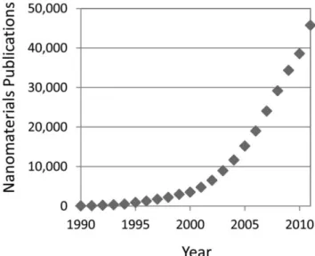
The origin of nanoscience usually is associated with a 1959 lecture by Richard Feynman [1]. Possibly, the first use of the term “nanotechnology” in the scientific literature was in a 1974 paper involving “ion-sputter machining” by Taniguchi [2]. The first nanotechnology journal, Nanotechnology, was launched in 1990 by the Institute of Physics in the United Kingdom. The number of publications related to nanotechnology mirrors the historical time line. Results from a Web of Science search combining the terms “nanomaterial,” “nanoparticle,” and “nanostructure” show dramatic growth in published papers (Figure 2.1), from less than 100 in 1990 to almost 45,000 in 2011.
Figure 2.1: Graph shows dramatic growth in published papers related to nanotechnology.
Nanotechnology is part of a natural progression in many different areas of science coupled with development of new tools that enable researchers to see, model, and control structures at the nanometer scale. Although, in many ways, nanotechnology is not new, experimental and computational tool development enables research to be done that was not previously possible. New approaches can be taken to address previously intractable problems. Therefore, nanoscience and nanotechnology do not represent a new discipline, but rather advancements within several disciplines and a convergence of concepts and ideas across disciplines. As such, nanotechnology introduces important new ideas and cross-fertilization that enables scientific breakthroughs and development of various new technologies.
3
Some of the most intriguing materials are those only a single atom thick. These two-dimensional materials, such as graphene and silicene, have attracted tremendous attention due to their unique physical and chemical properties. On the other hand, graphene is one of the allotropes of carbon that, together with fullerenes and carbon nanotubes, has determined was called the “carbon revolution”. One of the more important and promising carbon allotropes nowadays are the so-called “carbon nano-onions”, which are made of spherical or polyhedral concentric layers of carbon atoms arranged in a honeycomb net.
The purpose of this thesis was to synthesize and study Graphene, Silicene and Carbon Nano-Onions (CNO).
Graphene was obtained on a Ni(111) surface, and its plasmonic properties were studied by electron energy loss spectroscopy. Moreover, the structure of the carbon K-edge loss was measured and compared with theoretical results.
Silicene was synthesized on Ag(111) in different geometrical arrangements determined by LEED, and it has been shown that they have peculiar plasmonic properties. In particular, a Silicene layer made of a mix of three different phases seems to behave as a free-standing Silicene layer.
CNO were obtained by the underwater arc discharge technique. A new crystallization mechanism has been introduced to explain the formation of a conglomerate made almost exclusively of CNO which forms in the plasmatic zone.
4
1.1 Graphene
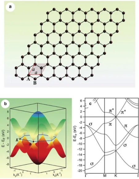
Graphene is a flat single layer of carbon atoms arranged in a honeycomb lattice with two crystallographically equivalent atoms (A and B) in its primitive unit cell [1–3] [Figure 2.2 a]. The sp2 hybridization between one 2s orbital and two 2p orbitals leads to a trigonal planar
structure with a formation of strong bonds between carbon atoms that are separated by 1.42 Å. The bonding orbitals have a filled shell and, hence, form deeper valence band levels. The 2pz
orbitals on the neighbouring carbon atoms are perpendicular to the planar structure of the graphene layer and can bind covalently, leading to the formation of a band.
Figure 2.2: (a) Crystal structure of the graphene layer, where carbon atoms are arranged in a honeycomb lattice. The unit cell of graphene with lattice constant a has two carbon atoms per unit cell, A and B. (b) Electronic dispersion of and states in the honeycomb lattice of free-standing graphene. (c) Band structure of free-standing graphene ( ,
5
The unique property of the electronic structure of graphene is that the π and π* bands touch at a single point at the Fermi energy (EF) at the corner of graphene‟s hexagonal Brillouin
zone, and close to this so-called Dirac point the bands display a linear dispersion and form Dirac cones [4] [Figure 2.2 b]. Thus, undoped graphene is a semimetal (“zerogap semiconductor”). The linear dispersion of the bands mimics the physics of quasi-particles with zero mass, the so-called massless Dirac fermions [1–3]. The fascinating electronic and transport properties of graphene [1–3] make it to a point of focus not only in fundamental research but also in applied science and technology with a vision to implement graphene in a myriad of electronic devices replacing the existing silicon technology.
However, a widespread implementation of graphene in electronics has been hampered by the two major difficulties: reliable production of high-quality samples, especially in a large-scale fashion and the “zero-gap” electronic structure of graphene, which leads to limitations for direct application of this material in possible electronic devices. As a response to the first challenge, a number of approaches for single layer graphene preparation have been tested, corroborating chemical vapor deposition (CVD) on transition-metal surfaces to be the most promising alternative to micromechanical cleavage for producing macroscopic graphene films. In 2008, mass-production of continuous graphene wafers by the CVD method on polycrystalline Ni or Cu surfaces and its transfer to arbitrary substrates was demonstrated [4–6]. The transferred graphene films show very low sheet resistance of 280 Ω per square, with 80% optical transparency, high electron mobility of 3,700 cm2V-1s-1, and the half-integer quantum Hall effect at low temperatures, indicating that the quality of graphene grown by CVD is as high as that of mechanically cleaved graphene. Further modifications of this method within less than one year led to even more fascinating results, where graphene layers as large as 30 inches were transferred on to a polymer film for the preparation of transparent electrodes [9].
Despite the fascinating recent achievements in graphene production, the second problem of controllable doping should be solved prior to being able to implement graphene in any kind of electronic device. Several strategies exist, which allow the modification of the electronic structure of graphene, including (1) fabrication of narrow, straight-edged stripes of graphene, so-called nanoribbons [8,9], (2) preparation of bi-layer graphene [10,11], (3) direct chemical doping of graphene by an exchange of a small amount of carbon atoms by nitrogen [14], boron [15] or
6
transition-metal atoms [16]; (4) modification of the electronic structure of the graphene by interaction with substrates [15–19]; (5) intercalation of materials underneath graphene prepared on different substrates [20–25]; (6) deposition of different materials on top of graphene [26–28]. Not surprisingly, the investigation of graphene interaction with supporting or doping materials, which may provide an additional important degree of control of graphene properties, has become one of the most important research fields [29–32].
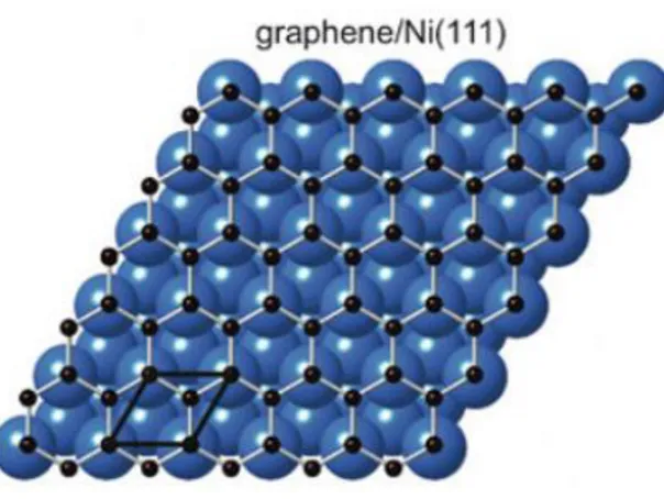
Figure 2.3: Top-view of a simple ball model for the top-fcc graphene/Ni(111) system is shown. Carbon atoms are
small black spheres and nickel atoms are big blue spheres.
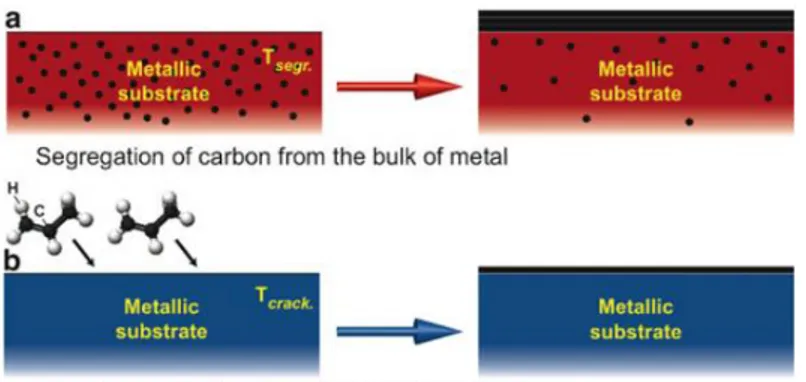
Two common methods of graphene preparation on metallic surfaces exist: (1) elevated temperature segregation of the carbon atoms to the surface of a bulk metallic sample, which was doped with carbon prior to the treatment [Figure 2.4 a] and (2) thermal decomposition of carbon-containing molecules on the surface of transition metals (TMs) [Figure 2.4 b]. In the first method, the transition-metal sample with some amount of carbon impurities or the bulk crystal previously loaded with carbon (via keeping the sample at elevated temperature in the atmosphere of CO or hydrocarbons) is annealed at higher temperatures. This procedure leads to the segregation of carbon atoms to the surface of the metal. Careful control of the temperature and the cooling rate of the sample allow varying the thicknesses of the grown graphene layer: monolayer versus multilayer growth.
7
Figure 2.4: Two ways of the graphene preparation on metal surfaces: (a) Segregation of bulk-dissolved carbon atoms to the surface at high temperature Tsegr; (b) Decomposition (cracking) of hydrocarbon molecules at the surface
of transition metals at high temperature Tcrack
The second method involves the thermal decomposition (cracking) of carbon-containing molecules at a metal surface. Light hydrocarbon molecules, such as ethylene or propene, are commonly used, but the successful decomposition of CO, acetylene, and of heavy hydrocarbon molecules, such as cyclohexane, n-heptane, benzene, and toluene, was also demonstrated [17]. Molecules can be adsorbed on a metal surface at room temperature, and then annealing of the sample leads to the decomposition of molecules and hydrogen desorption. Alternatively, the hot sample surface can be directly exposed to precursor molecules, which decompose at the sample surface. Recent experiments demonstrate that both methods, segregation and decomposition, lead to graphene layers of similar quality. In case of segregation, the kinetics of single graphene layer formation is defined by a careful control of the annealing temperature (but multilayers of graphene could also be prepared). In the second method, the graphene thickness is naturally restricted to a single-layer due to the fact that the chemical reaction on the catalytically active metallic surface takes the place. Thus, the speed of hydrocarbon decomposition drops down by several orders of magnitude as soon as the first graphene monolayer is formed [33,34].
8
1.2 Silicene
Silicene is a single atomic layer of silicon much like graphene [37]. Early work, both theoretical [2–6] and experimental [7,8] , went mostly unnoticed until silicene nanoribbons were reported to have been fabricated on a silver substrate [45]. Since then, silicene sheets have been grown mainly on Ag(111) [10–14]; these were achieved under ultrahigh vacuum conditions by evaporation of silicon wafer and slow deposition onto a substrate at 220–260 °C.
The interest in silicene is exactly the same as that for graphene, in being two-dimensional (2D) and possessing Dirac cones [51]. One advantage relies on its possible application in electronics, whereby its natural compatibility with the current Si technology might make fabrication a commercial reality. Indeed, a field-effect transistor made out of silicene has finally been demonstrated in 2015 [52].
Although theorists had speculated about the existence and possible properties of silicene, [15,17,18] researchers first observed silicon structures that were suggestive of silicene in 2010 [19,20]. Using a scanning tunneling microscope they studied self-assembled silicene nanoribbons and silicene sheets deposited onto a silver crystal, Ag(110) and Ag(111), with atomic resolution. The images revealed hexagons in a honeycomb structure similar to that of graphene which, however, were shown to originate from the silver surface mimicking the hexagons [57]. Density functional theory (DFT) calculations showed that silicon atoms tend to form such honeycomb structures on silver, and adopt a slight curvature that makes the graphene-like configuration more likely. This was followed by the discovery of dumbbell reconstruction in silicene [58] which explains the formation mechanisms of layered silicene [59] and silicene on Ag [60]. In 2015, a silicene field-effect transistor made its debut [61] that opens up new opportunities for two-dimensional silicon for various fundamental science studies and electronic applications [26,27].
Similarities with graphene come from the similar atoms of silicon and carbon. They lie next to each other in the same group on the periodic table and have an s2 p2 electronic structure. The 2D structures of silicene and graphene also are quite similar but have important differences [64]. While both form hexagonal structures, graphene is completely flat, while silicene forms buckled hexagonal layers. Its buckled structure gives silicene a tuneable band gap by applying an
9
external electric field. Silicene's hydrogenation reaction is more exothermic than graphene's. Another difference is that since silicon's covalent bonds do not have pi-stacking, silicene does not cluster into a graphite-like form [65].
Silicene and graphene have similar electronic structures. Both have a Dirac cone and linear electronic dispersion around the Γ point. Both also have a quantum spin Hall effect. Both are expected to have the characteristics of massless Dirac fermions that carry charge, but this is only predicted for silicene and has not been observed, likely because it is expected to only occur with free-standing silicene which has not been synthesized. It is believed that the substrate silicene is made on has a substantial effect on its electronic properties [65].
Unlike carbon atoms in graphene, silicon atoms tend to adopt sp3 hybridization over sp2 in silicene, which makes it highly chemically active on the surface and allows its electronic states to be easily tuned by chemical functionalization [66].
2D silicene is not fully planar, apparently featuring chair-like puckering distortions in the rings. This leads to ordered surface ripples. Hydrogenation of silicenes to silicanes is exothermic. This led to the prediction that the process of conversion of silicene to silicane (hydrogenated silicene) is a candidate for hydrogen storage. Unlike graphite, which consists of weakly held stacks of graphene layers through dispersion forces, interlayer coupling in silicenes is very strong. The buckling of the hexagonal structure of silicene is caused by pseudo-Jahn-Teller distortion (PJT). This is caused by strong vibronic coupling of unoccupied molecular orbitals and occupied molecular orbitals. These orbitals are close enough in energy to cause the distortion to high symmetry configurations of silicene. The buckled structure can be flattened by suppressing the PJT distortion by increasing the energy gap between the unoccupied molecular orbitals and occupied molecular orbitals. This can be done by adding lithium ions [65]. In addition to its potential compatibility with existing semiconductor techniques, silicene has the advantage that its edges do not exhibit oxygen reactivity [67].
In 2012 several groups independently reported ordered phases on the Ag(111) surface [11,13,14]. Results from scanning tunneling spectroscopy measurements [68] and from angle-resolved photoemission spectroscopy (ARPES) appeared to show that silicene would have
10
similar electronic properties as graphene, namely an electronic dispersion resembling that of relativistic Dirac fermions at the K points of the Brillouin zone, [50] but the interpretation was later disputed and shown to arise due to a substrate ban [33–39]. The p-d hybridisation mechanism between Ag and Si is important to stabilise the nearly flat silicon clusters and the effectiveness of Ag substrate for silicene growth explained by DFT calculations and molecular dynamics simulations [38,40]. The unique hybridized electronic structures of epitaxial 4×4 silicene on Ag(111) determines highly chemical reactivity of silicene surface, which are revealed by scanning tunneling microscopy and angle-resolved photoemission spectroscopy. The hybridization between Si and Ag results in a metallic surface state, which can gradually decay due to oxygen adsorption. X-ray photoemission spectroscopy confirms the decoupling of Si-Ag bonds after oxygen treatment as well as the relatively oxygen resistance of Ag(111) surface, in contrast to 4×4 silicene [with respect to Ag(111)] [74].
11
1.3 Carbon nano-onions (CNO)
Beginning with the discovery of fullerenes (1985) [77], moving to carbon nanotubes in (1991) [78], and then to graphene in (2004) [37], carbon nanomaterials have been widely studied and have shown to have a multitude of potential applications. However, another unique allotropic form of carbon, Carbon Nano Onions (CNOs) [3–9], which was actually discovered before these other materials, has long been overshadowed by these more popular and much more thoroughly investigated carbon nanomaterials.
CNOs consist of multilayered quasi-spherical and polyhedral shaped shells that represent another new nanophase of carbon material that owes its name to its concentric layered structures resembling that of an onion [80]. In the last several years, CNOs have attracted a great deal of attention because of their unique chemical and physical properties. These properties are different from those of other nano-sized carbon materials.
CNOs have been extensively studied to understand their underlying nature and to explore their potentiality for a wide variety of technological applications [81]. Although CNOs has been synthesized by many different methods in the last 30 years, large scale production has yet to be fully achieved.
Sumio Iijima first discovered CNOs while looking at a sample of carbon black in a transmission electron microscope (TEM) in 1980 [84]. The small amount of CNOs that were created in vacuum was observed as a byproduct of the synthesis of carbon black. From then until today the methods that have been developed to synthesize CNOs still remain in their infancy and suffer from issues relating to quality, quantity and purity. Various synthesis pathways have led to discoveries of CNOs with unique physical properties including varying shell numbers, graphitic structures, core types, and precursors.
Twelve years after the first discovery of the CNOs, Daniel Ugarte (1992) [79] is credited with developing a formation mechanism for the creation of spherical graphitic structures by focusing an electron beam on a sample of amorphous carbon. This process caused the carbon to graphitize and began to curl. After sufficient time, it closed on itself forming an onion like
12
structure. It is surmised that the curving and closure occurred in order to minimize the surface energy of the newly formed edge planes of graphite.
Because of its multitude of applications, it is of paramount importance to be able to synthesize this material economically in consistent size, high purity and large volume. According to the literature available, to date, the method that is the most utilized is the thermal transformation of nanodiamonds in vacuum [83]. According to published claims, the material can be made in sizeable volume using this method, as opposed to the very limited volume production of the other above mentioned processes. CNOs can also be produces by DC underwater arc discharge between graphite electrodes [83,84].
Recently, Bartelmess and Giordani published an extensive review on the development of carbon nano onions (CNOs) and the many pathways (over the years) that have been used to synthesize this material [87]. CNOs have even attracted the interest of NASA researchers for their tri-biological properties as additives for aerospace applications. Despite much interest in different carbon-based nanomaterials, CNOs as functional constructs for intracellular transport have not been widely explored. However, given their size, homogeneity and purity (compared with carbon nanotubes) they could in principle add an important new avenue for the transport of imaging and therapeutic agents. These carbon particles have demonstrated a higher cellular uptake, low cytotoxicity and lower inflammatory potential, than CNTs, thus creating a very promising future for their biomedical applications.”
CHAPTER TWO
EXPERIMENTAL
METHODS
14
2.1 Ultra-High Vacuum (UHV) Chamber
UHV is a necessary condition for many surface analytic techniques to reduce surface contamination, by reducing the number of molecules reaching the sample over the time period necessary to perform investigation. Moreover, surface-sensitive spectroscopies utilize electron beams and analyzers that need ultra-high vacuum conditions. Typically, UHV requires high pumping speed, possibly multiple vacuum pumps in series and/or parallel.
Figure 2.1: Ultra High Vacuum Chamber in Nanoscience Laboratory
The UHV chamber used in this work is divided into two communicant sections as we have in Figure 2.1. In the upper section we performed Electron Energy Loss Spectroscopy (EELS), Low Electron Energy Diffraction (LEED) and X-Ray Photoelectron Spectroscopy (XPS). For these purposes, the upper part is equipped with an electron gun, an X-Ray source (Al K, 1486.6 eV), an hemispherical electron energy analyzer that can collect the electrons emitted (or scattered) by the sample, and a Retarding Field Analyzer for LEED measurements. In the upper section are also present three gas-lines for the controlled release of gases in the analysis chamber, and an ion gun that generates a beam of argon ions.
15
The lower part of the UHV chamber contains an apparatus for High Resolution Electron Energy Loss Spectroscopy (HREELS) made of a fixed monochromator and a rotating analyzer, both 50 mm electrostatic hemispherical. The angular acceptance of the analyzer is 2°.
2.2 Low Energy Electron Diffraction (LEED)
LEED is a technique that allows to gain information about the long range order of atoms at the surface of a crystal through the diffraction of electrons with low energy. LEED permits the determination of the surface symmetry of single-crystalline materials by bombardment with low energy electrons and observation of diffracted electrons as spots on a fluorescent screen (Figure 2.2).
Figure 2.2: Picture of low energy electron difraction apparatus.
The LEED detector usually contains an electron gun, three or four hemispherical concentric grids (the Retarding Field Analyzer) and a phosphor screen. Electron gun can produce electrons with energy from 20 to 200 eV, the electrons are emitted by a cathode filament which is at a negative potential with respect to the sample. The electrons are accelerated and focused into a beam, with a typical width that extends from 0.1 to 0.5 mm. Some of the electrons incident on the sample surface are backscattered elastically, and diffraction can be detected when the sample has an ordered surface. The grids are used for screening out the inelastic scattered electrons (Figure 2.3); therefore the first grid screens the space above the sample from the
16
retarding field, the next grid is at a potential to block low energy electrons, it is called the suppressor and is a retarding field analyzer to block inelastically scattered electrons.
Figure 2.3: Diagram of Low Energy Electron Diffraction apparatus.
Only the elastically scattered electrons are accelerated and hit a fluorescent screen producing the projecting of the reciprocal lattice of the sample (diffraction LEED pattern). The electron beam can be represented by a plane wave with a wavelength in accordance to the de Broglie hypothesis:
λ=
√
, λ [
nm] ≈√
The interaction between the scattering centers present in the surface and the incident electrons is most conveniently described in reciprocal space. In three dimensions the primitive reciprocal lattice vectors {a*, b*, c*} are related to the real space lattice {a, b, c} in the following way:
a* = b* = c* =
17
For an incident electron with wave vector k0=2π/λ0 and scattered wave vector k=2π/λ, the
condition for constructive interference and hence diffraction of scattered electron waves is given by the Laue condition:
k-k0 = Ghkl,
where, (h,k,l) is a set of integers and Ghkl=ha*+kb*+lc* is a vector of the reciprocal lattice
(Figure 2.4). The magnitudes of the wave vectors are unchanged, i.e. │k0│=│k│, since only
elastic scattering is considered. Since the mean free path of low energy electrons in the matter is only a few angstroms, only the first few atomic layers contribute to the diffraction. This means that there are no diffraction conditions in the direction perpendicular to the sample surface. As a consequence the reciprocal lattice of a surface is a 2D lattice with rods extending perpendicular from each lattice point.
Figure 2.4: Ewald's sphere construction for the case of diffraction from a 2D-lattice.
2.3 X-ray Photoelectron Spectroscopy (XPS)
The main component of a XPS system include a source of X-rays, based on the fluorescent emission of photons from a magnesium or aluminum slab caused by high energetic electrons emitted by a filament and accelerated towards the anode by a voltage of the order of some KeV. Non-monochromatic magnesium X-rays have a wavelength of 9.89 angstroms which corresponds to a photon energy of 1253 eV. The energy width of the non-monochromatic X-ray
18
is roughly 0.70 eV, which is the ultimate energy resolution of a system using non monochromatic X-rays.
The mean free path of electrons in solids is very small, the detected electrons originate from only the top few atomic layers, making XPS a surface-sensitive technique for chemical analysis. Quantitative data can be obtained from peak heights or peak areas and identification of chemical states often can be made from exact measurements of peak positions and separations. Each element has a unique set of binding energies, XPS can be used to identify and determine the concentration of the elements in the surface. Variations in the elemental binding energies (chemical shifts) arise from differences in the chemical potential and polarizability of compounds. These chemical shifts can be used to identify the chemical state of the materials being analyzed.
A schematic figure about an experimental setup of photoelectron spectroscopy can be seen in Figure 2.5 below consisting of 3 main parts: X-ray source, UHV vacuum system and detection & analyzer system.
Figure 2.5: Schematic figure of an XPS system.
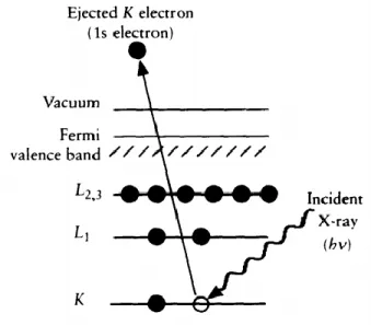
In XPS we are concerned with a special form of photoemission, i.e., the ejection of an electron from a core level by an X-ray photon of energy hv. The energy of the emitted
19
photoelectrons is then analysed by the electron spectrometer and the data presented as a graph of intensity versus electron energy – the X-ray induced photoelectron spectrum.
The kinetic energy (EK) of the electron is the experimental quantity measured by the
spectrometer, but this is dependent on the photon energy of the X-rays employed and is therefore not an intrinsic material property. The binding energy of the electron (EB) is the parameter which
identifies the electron specifically, both in terms of its parent element and atomic energy level. The relationship between the parameters involved in the XPS experiment is:
EB= hv - EK – W
where h is the photon energy, EK is the kinetic energy of the electron, and W is the spectrometer
work function. As all three quantities on the right-hand side of the equation are known or measurable, it is a simple matter to calculate the binding energy of the electron. In practice, this task will be performed by the control electronics or data system associated with the spectrometer and the operator merely selects a binding or kinetic energy scale whichever is considered the more appropriate. [88]
Figure 2.6: Schematic diagram of the XPS process, showing photoionization of an atom by the ejection of a 1s electron
20
The process of photoemission is shown schematically in Figure 2.6, where an electron from the K shell is ejected from the atom (a 1s photoelectron). The photoelectron spectrum will reproduce the electronic structure of an element quite accurately since all electrons with a binding energy less than the photon energy will feature in the spectrum.
2.4 Electron Energy Loss Spectroscopy (EELS)
EELS is one of the most common surface analysis techniques used to investigate the excitations in a crystal, caused by an incident electrons beam called primary beam, by analyzing the energy spectrum of electrons backscattered from it. An electron passing through material can interact with electron clouds of the atoms present and transfer some of its kinetic energy to them. There are two modes of operating for EELS:
1. Electron Energy Loss Spectroscopy in transmission mode. 2. Electron Energy Loss Spectroscopy in reflection mode.
EELS in transmission mode uses electrons at energies of the order on tenths of keV. At those high energies, the incident electrons beam passes through a thin foil of the material of interest and the transmitted one contains inelastically scattered electrons whose energy has been decreased by amounts corresponding to characteristic absorption energies in the solid. At lower primary energies, (from few to hundreds of eV) the Electron Energy Loss Spectroscopy is used in the reflection mode, in this approach the reflected beam is monitored for the electronic excitations occurred in the surface. Bulk and surface plasmons are the principal features of these spectra.
High Resolution EELS employs a monochromatic incident electron beam of quite low energy (a few eV). The primary focus of this technique is the study of vibrational structure of the surface and especially of adsorbents on that surface.
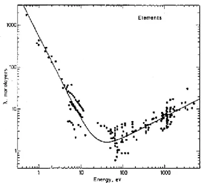
The energy of the primary beam has fundamental importance to understand how deep the sample is probed, in fact Figure 2.7 represents the mean free path (counted in monolayers) versus the energy of the incident electron beam.
21
Figure 2.7: Electrons mean free path as function of their energies.
The mean free path, that is the mean distance covered by an electron in a medium before to undergo an inelastic collision, shows a minimum around 50 eV, and after this minimum, increasing primary energy implies the increasing of the mean free path. This graph is universal, it means that it‟s a good estimate of electrons mean free path in all medium, and also shows that for probe more than 10 monolayers (10-20 Å) of materials it‟s necessary to use electrons of more than 1000 eV of energy; therefore, all our measurements, carried out at a primary energy of about 100 eV, characterized mainly the surface properties of the sample. Similarly, also measurements obtained by X-Ray excitation source are surface sensitive, in fact, as assumed above, although the photons can penetrate more and more than the electron probe, the analyzer scans only the electrons coming from the outer layers very near to the surface of the sample.
In electron energy-loss spectroscopy, we deal directly with the primary process of electron excitation, which results in the fast electron losing a characteristic amount of energy. The electron beam scattered by the sample is directed into a high-resolution electron spectrometer that separates the electrons according to their kinetic energy and produces an electron energy-loss spectrum showing the number of electrons (scattered intensity) as a function of their decrease in kinetic energy.
22
The scattered electrons have principally the same energy of the incident electron beam (elastic peak) and only few electrons are emitted with lower energy respect to the primary energy. These latter are inelastic electrons and the energy they lost (Eloss) is the same energy that
the crystal absorbed to produce an excitation.
The sample excitations induced by an electronic perturbation, are mainly divided into three groups, each for a specific energy range:
1. Core electron excitations (Eloss of the order of hundreds of eV)
2. Valence band excitations (single particle interband or intraband transitions), surface and bulk collective excitations (plasmons) (Eloss of the order of tens of eV).
3. Vibrational excitations of the sample (acoustic and optic phonon) and vibrational excitations of atoms or molecules adsorbed on the surface (Eloss of the order of meV).
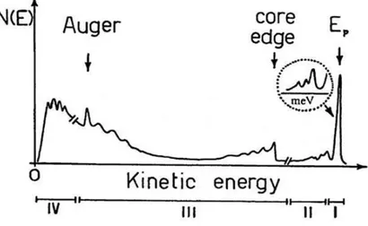
Figure 2.8: Energy of the electrons emitted after the interaction with a beam of primary electrons of energy Ep.
In Figure 2.8 is plotted the typical energy distribution N(E) of the electrons emitted by the crystal after the interaction with a beam of primary electrons of energy Ep. The previous figure
can be divided in four sections, each of which represents different ranges of Eloss with different
sample information:
The region I includes the highest peak of the energy distribution with energy Ep that is the
elastic peak and allows finding information about the structure of the sample. It contains all electrons that have suffered an elastic interaction only. The peaks close to the elastic peak
23
(within about 1 eV) allow to gain information about the vibrational modes of the crystal (phonons) and the vibrational excitations of atoms and molecules adsorbed on the surface.
In the second region (II) it is possible to distinguish all the electrons that had inelastic interaction with the solid. The EELS spectroscopy is used, in this energy range, to have information about surface and bulk collective excitations and therefore about its dielectric function. Here, the plasmon peaks are the predominant features.
The third region (III) contains electrons which suffered higher energy losses and secondary electrons at high energy. Ionization edges appear at electron energy losses that are typical for a specific element and thus qualitative analysis of a material is possible by EELS. The onset of such an ionization edge corresponds to the threshold energy that is necessary to promote an inner shell electron from its energetically favored ground state to the lowest unoccupied level. This energy is specific for a certain shell and for a certain element. Above this threshold energy, all energy losses are possible since an electron transferred to the vacuum might carry any amount of additional energy. If the atom has a well-structured density of states (DOS) around the Fermi level, not all transitions are equally likely. This gives rise to a fine structure of the area close to the edge that reflects the DOS and gives information about the bonding state. This method is called electron energy loss near edge structure (ELNES). From a careful evaluation of the fine structure farther away from the edge, until hundreds eV above the core excitations, information about coordination and interatomic distances are obtainable (extended energy loss fine structure, EXELFS).
In the last region (IV) is an high and wide peak caused by the secondary electrons, also this peak has a fine structure that can be analyzed by the angle-resolved Secondary Electron Emission (SEE). This analysis provides information about the density and the dispersion of empty states just above the Fermi level.
There are several basic flavors of EELS, primarily classified by the geometry and by the kinetic energy of the incident electrons. Probably the most common today is transmission EELS, in which the kinetic energies are typically 100 to 300 keV and the incident electrons pass entirely through the material sample. Usually this occurs in a transmission electron microscope (TEM),
24
although some dedicated systems exist which enable extreme resolution in terms of energy and momentum transfer at the expense of spatial resolution.
Instead, the reflection geometry is particularly sensitive to surface properties but is limited to very small energy losses such as those associated with surface plasmons or direct interband transitions. Lucas and Sunjc [89] made the first publications about this, followed by Evans e Mills [2– 4].
The EELS spectroscopy has several analogies with optic absorption, in fact both techniques give information about the density of electronic bands in the examined solid. EELS, however, makes it possible to change easily the energy of the incident beam, in order to probe a larger energy range. Furthermore, the low mean free path of electrons in the reflection geometry makes this technique more sensible to the surface proprieties with respect to optical spectroscopy.
2.4.1 Theoretical Fundaments
In a continuous and homogeneous medium, the response to an electric external perturbation can be described by the dielectric theory. When an electron approaches a dielectric material, the electron density inside the solid changes to shield the long range electric field produced by the incoming perturbation. The density fluctuations generated inside the medium are related to the wave vector and the frequency of the external field, so the transferred energy depends on the field density energy variation inside the solid.
An electron inside the solid can acquire energy and impulse , because of inelastic interaction with an incident electron, if it lost the same amount of energy .
The incident electron can be described by the electronic distribution:
The interaction potential produced inside the solid, follows the Poisson equation:
25
The energy loss of the electron in length unit inside the medium is , where is
the component of the electric field along the x axis, perpendicular to the surface. Whereas ∫ ∫
Replacing in this equation, the expression found for we obtain the loss energy probability in length unit as function of the exchanged moment and of the frequency :
where *
+ is the bulk loss function.
So the bulk loss function describes the inelastic interaction of high energy electrons that pass through the sample.
A maximum in the loss function occurs when and . One can see that the condition under which corresponds to the excitation of a plasma wave in the medium.
The most used models to describe a solid material are the Drude and Lorentz models [93]. The first one deals the conduction electrons as a free electrons gas not subject to atomic potential, and in this case the dielectric function, in the limit of , is:
⁄
where is the plasma frequency and is the relaxing time that takes into account the interactions between the electrons.
26
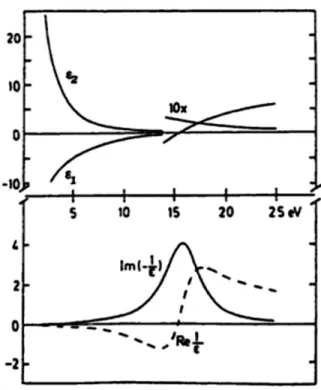
Figure 2.9: Real and imaginary part of the dielectric function ε (upper side) and real and imaginary part of 1/ ε (bottom side) for the Drude model.
The imaginary part of the dielectric function (Figure 2.9), is monotonically decreasing and does not exhibit any structure, so a free electron gas does not generate any optical absorption. The loss function, instead, exhibits a maximum at the plasma frequency , corresponding to the excitation energy of a bulk plasmon in a free electron gas (from several eV to few tens of eV).
Lorentz model is based on treating electrons as damped harmonically bound particles subject to external electric fields. This model describes successfully bound electrons in a solid interacting with an electric field E and affected by an elastic-like restoring force with a own resonance frequency . Furthermore, to adapt, this ideal model to the experimental reality, the existence of a viscous term is assumed that can explain the linewidths experimentally observed and avoid annoying divergences. The real materials have different resonances with different intensities, so it is associated at the resonance frequency , an empirical parameter called oscillator strength factor through which it possible to weigh the different intensities, so it satisfies the relation:
27 ∑
To obtain the Lorentz oscillator relation, in the single resonance frequency case, we start from the second law of dynamics:
̈ ̇
Where is the electron mass, is the electron charge and is the electron external field applied to the material. Solving the equation for and replacing the external field by , it is obtained:
( ⁄ )
Using the equations for the microscopic dipole and for macroscopic polarization it is extracted:
( ⁄ )
Knowing that polarization and electric field are related through the equation the dielectric function, for just one type of transition is
where √
is the plasma frequency and is the oscillator strength factor. So for
different resonances the real and imaginary part of the dielectric function, respectively and , are:
28
∑
∑
Generally this is a good approximation for semiconductor, insulators and for all metals which possess bound electrons (d or p valence electrons).
The following figure reports , [ ⁄ ] and [ ⁄ ] calculated for the Lorentz model
Figure 2.10: Real and imaginary part of the dielectric function ε (upper side) and real and imaginary part of 1/ ε (bottom side) for the Lorentz model.
In Figure 2.10 , the peak in function represents an optical absorption at , while the loss function exhibits a maximum at a frequency > where and The occurrence of these conditions corresponds to a collective excitation in the solid known as “interband plasmon” in analogy to the free electron model.
29
More generally the behavior of metals is described by a dielectric function that is the sum of the intraband type (Drude model) and the interband type (Lorentz model). So the dielectric function is described by:
Observing trends of and [ ⁄ ] for metals and semiconductors, it‟s clear that the maximum of these two function are never in the same energy position, on the contrary we can assume that the maximum of matches with the minimum of [ ⁄ ], like if
[ ⁄ ] ⁄ .
In conclusion this is the evidence that the single particle excitations and the collective excitations are generally in competition, making the EEL probability, in the range of 1-20 eV, inversely proportional to the optical absorption.
2.4.2 EELS in reflection geometry
The schematic representation of the EELS in reflection geometry is shown in the following Figure 2.11.
Figure 2.11: EELS reflection geometry representation
We assume that an electron with energy and wave vector hits the sample at an angle of incidence with respect to the surface normal and it scatters off the crystal with energy and wave vector at an angle .
30
We are describing an inelastic process, so the incident electron can transfer energy ( )
and momentum ( ) to the sample. From the conservation rule of energy we know that:
The conservation of the component parallel to the surface of the momentum is more restrictive, in fact just the component parallel to the surface must be preserved. So, we have:
Therefore, the component parallel to the surface of the momentum transfer is calculated as:
| |
Taking into account the relation between the energy and the momentum for a free electron
we can calculate | |:
| | √ (√ √ )
Thus, using monochromatic electron beam with a rotating analyzer it is possible, for each loss energy, calculate the component parallel to the surface of the momentum transfer obtaining the energy dispersion curve of the observed loss .
2.5 Raman Spectroscopy
Raman spectroscopy is a spectroscopic technique based on inelastic scattering of monochromatic light, usually from a laser source (Figure 2.12.a). Inelastic scattering means that the frequency of photons in monochromatic light changes upon interaction with a sample. Photons of the laser light are absorbed by the sample and then reemitted. The frequency of part of the reemitted photons is shifted up or down with respect to the original monochromatic