C
ATANIA
F
ACOLTÀ DI
I
NGEGNERIA
C
ORSO DI
D
OTTORATO DI
R
ICERCA IN
I
NGEGNERIA
E
LETTRONICA
,
A
UTOMATICA E DEL
C
ONTROLLO DEI
S
ISTEMI
C
OMPLESSI
Salvatore Tomarchio
Power Switching Converters with very
low power consumption and high
efficiency for energy savings
Relatore:
Chiar.mo Prof. Ing. Angelo Raciti Coordinatore:
Chiar.mo Prof. Ing. Luigi Fortuna
Page | I
Chapter 1
Defining the objectives of the research………... Page 1 1. Introduction……….... Page 2
Chapter 2
Sustainable development……….. Page 4 2. Introduction……… Page 5 2.1. Energy waste and power consumptions……… Page 6
Chapter 3
Energy saving regulations……… Page 9 3. Introduction……….. Page 10 3.1. Reference to the regulation on the appliance field………. Page 10 3.1.1. Measurement’s method of power consumption – EN 62301………. Page 12 3.1.1.1. Subject of the regulation……….... Page 13 3.1.1.2. Procedure of measurement………. Page 15 3.1.1.3. Low power measurement………... Page 17 3.2. Reference to the regulation on the lighting field………... Page 18
Chapter 4
Analysis of power converter for LED lamps………. Page 21 4. Introduction………. Page 22 4.1. Improvement of LED technologies……….... Page 23
Page | II
4.2.1.1. Flyback converter………..………... Page 25 4.2.1.2. Resonant converter………... Page 33 4.2.2. Non isolated topologies………... Page 33 4.2.2.1 Buck converter………..….…….…. Page 34 4.2.2.2 Boost converter ………..…..….…….. Page 34 4.2.2.3 Zeta converter……….………. Page 35 4.2.3. Analysis of the results……….….…………. Page 36
Chapter 5
Analysis of the conventional techniques to reduce
the power consumption of appliances……….……….…. Page 37 5. Introduction.………..……….. Page 38 5.1. Start up circuit……….…….…………. Page 38 5.2. Switching frequency reduction………..…….………... Page 38 5.2.1. Effective switching frequency reduction……….……….. Page 39 5.3. Output voltage disconnection……….….………….. Page 40 5.4. Output voltage drop………..…... Page 40 5.5. Output voltage drop with auxiliary winding………...…….……. Page 41 5.6. Auxiliary Power supply………..……... Page 42 Chapter 6
Design of a 5W SMPS for Appliance field……….…….. Page 43 6. Introduction………..…... Page 44 6.1. Project requirements………... Page 44
Page | III
6.4. Design of passive components……….. Page 50 6.4.1. Transformer………... Page 50 6.4.2. Output capacitors……….…...…... Page 59 6.4.3. Snubber network……….……... Page 61 6.4.4. Input filter………...…... Page 64 6.5. Design of active components………...….. Page 65 6.5.1. Design of the output rectifier diode and snubber’s diode………... Page 66 Chapter 7
Analysis and Design of a circuit to control the state of the SMPS………..…... Page 68 7. Introduction………..…... Page 69 7.1. Electrical circuit analysis……….….…….. Page 69 7.2. Circuit design………..….... Page 71 7.3. Simulation and experimental measurements………..…..….. Page 73
Chapter 8
Development of a prototype and experimental measurements……….…... Page 79 8. Introduction……….….... Page 80 8.1. Electrical schematics………... Page 80 8.2. Test for project validation……….. Page 82 8.2.1. Measurements of the electrical specifications……….……. Page 82 8.2.2. Thermal analysis in climatic chamber at hard condition…….……. Page 89 8.3. Analysis of the results………..….. Page 97
Page | IV
Supply for Gate Driving Applications………... Page 98 9. Introduction………. Page 99 9.1. The buck converter design………..…….. Page 100
9.1.1. Main circuit requirements for IGCT GU supply…………...…….. Page 101 9.1.2. Design of power switches and passive components………...……. Page 101 9.1.3. Series connection………. Page 104 9.2. Experimental validation……… Page 107 9.3. Discussion……… Page 118
Chapter 10
Conclusions ………. Page 119
I. Appendix
The Flyback Converter……….……... Page 122 A. Introduction……….….... Page 123 B. Operation modes……….……. Page 125 C. Waveform of the voltage drop on the power switching device…………... Page 132 Bibliography………..….. Page 134
Chapter 1
1. Introduction
The objective of this research is the analysis of power switching converters with targets of very low power consumption and high efficiency for being used in new system for energy savings.
Typically, they are implemented as Switching Mode Power Supply (SMPS) modules in different type of applications in both consumer and energy businesses.
In particular have been considered power supply systems with output power in the class of low and medium power, in the range from few watts up to hundreds watts.
Referring to consumer business, the main fields of application are lighting and home appliances where in the last years the international Agencies and Governments have been focused their attention to ask for reducing the continuous energy waste.
Therefore, more restricted and challenging constraints have been fixed in order to reduce the energy waste and to improve the level of performances of new products, that pushed the introduction of new technologies and new design solutions.
In particular in the lighting applications the improvement in LED technologies is leading to the development of LED lamps with higher light efficiency and lower power consumption.
Appropriate electronics circuits are used in order to make the LED supply compatible with energy that is provided by the electrical main, 230 VAC @ 50 Hz. Thus a low DC voltage drives a small number of LED diodes in series connection. The most important requirements of the power converters for LEDs is a low ripple current, because it may cause changes in the light emitted from the diode (flickering). Also important are low power losses, high power factor and dimming capability.
The analysis will start making an overview of the principal topologies of switching converters used to drive the LED bulbs. Advantages and disadvantages will be shown for each topology. Then the flyback topology will be analyzed and discussed in more details, since it is considered the most promising one. Finally, an alternative schematic will be proposed in order to increase the electrical performance of the whole power conversion system.
On the other side in the home appliance applications there are conditions where the energy is consumed by the device when this does not work or does not perform its main functions and that happens without the final user realizing it. One condition is when the device is put in standby status.
For this case the analysis of the commonly used techniques for reducing power consumption in the switching converter is discussed and a new technique for reducing power during the inactivity state of the appliance system is proposed.
The proposed solution works on the feedback network, introducing a perturbation on the feedback signal: in this way the main power transistor, in the converter, is switched off and the output voltage of the converter is settled to zero. This solution allows an important reduction of the effective power consumption of the system.
In order to confirm this solution an auxiliary SMPS with output power of 5 W to supply the user interface of a washing machine has been designed, and the converter topology used is a Flyback converter, compliant with the current regulations of the home appliance applications.
In addition a prototype is realized and then simulations in PSpice, thermal and electrical measurements are performed in order to verify the operations of the converter in different environmental and electrical conditions.
Looking at the business of energy conversion, in the design of applications of high power systems an important issue is to provide low voltages, in the range of tens of Volt, tapping from high voltage input line, which is usually in the range between hundreds of Volt to kilovolt, by means of switching power supplies. Low voltages are needed to supply the logic control circuits and the power semiconductors driving the applications. The supply system has to deal, consequently, with both wide input voltage range and electrical insulation. The evaluation of the operative conditions of a driving system for IGCT devices, used in a transmission system application with wide input voltage range, is described. The design of a 100 W supply converter is shown considering all the issues related with the series connection of power devices and the needs of insulation.
Converter design, modelling and experimental results are shown together with the evaluation of the efficiency of the proposed solution.
Chapter 2
2. Introduction
The earth is suffering more and more from the damage due to the pollution resulting from the use of fossil fuels for energy production.
The most important portion of consumption of the natural resource and energy in the Community is due to the products energy consumption. Also these products provide a number of other important environmental impacts and for these reasons as well as to make more widespread use of renewable energy sources, is important to learn how to save energy.
In particular, the electricity demand is characterized by a fast growth and it is forecasted to growing over the next 20-30 year, in absence of a policy to counteract this trend. Developed countries are the most responsible ones both for the pollution and the depletion of energy resources because, with 25% of the world population, they consume each year over 75% of the available energy. For this reason it is very important to sensitize not only the industry, but also consumers in industrialized countries.
The energy that is used for civil use (non-industrial) is approximately 20% of that consumed in total; exists therefore a large amount of energy that can be spared. However, without making strong sacrifices, and simply changing the daily behaviour, it has been estimated that a family could save:
- 15% of heating costs
- More than 10% of cost for household appliances - 20% of cost for gasoline
For the majority of product categories available in the Community market can be observed very different levels of environmental impact, although their functional performances are similar.
In order to promote the sustainable development a continuous improvement in the overall environmental impact of those products should be encouraged, in particular identifying the major sources of negative environmental impacts and avoiding the transfer of pollution, when this improvement does not involve excessive costs.
The eco-design of products is a crucial factor in the community strategy that is finalized to the improvement of the environment performance of products and in the same time to keep the quality for the manufacturer, consumer and the society on together.
The improvement of the energy efficiency, which includes the most efficient use of the electricity, is considered a very important contribution in order to achieve the goals of emission reduction of the greenhouse gases in the Community.
It is needed acting as soon as possible in the design phase of a product that consumes energy (EuP), in order to define and control the level of pollution caused during the life cycle of the product and to find solutions to reduce that during this stage when most of the costs are taken up.
For this purpose, the Directive 2005/32/CE seeks to achieve a high level of prevention by reducing the potential environmental impact of the energy-using product, this results a benefit for the final consumers [1].
Furthermore, the Directive provides the setting of requirements which the energy using products, covered by implementing measures, must fulfil in order to be placed on the market and / or putting them in service.
It contributes to the sustainable development by increasing the energy efficiency and the level of environmental protection, and in the same time improving the security of energy supply.
2.1. Energy waste and power consumptions.
There are situations in which the energy is used even if the user doesn’t realize it. One of these is just leave the device in stand-by mode.
Energy is the average power multiplied by the time. Electrical energy is generally expressed in watt-hours or kilowatt-hours. Energy can also be expressed in joules.
One watt is the rate of energy consumption of 1 J/s and 1 kWh is equivalent to 3.6 MJ. To convert power to energy (an annual energy consumption), the number of hours of operation in each mode must be assumed for a given period and the average power for each mode must also be known. As most appliances can operate in a number of modes and the usage patterns and profiles may considerably vary between countries, converting power values determined under this standard to energy is potentially fraught with difficulty.
In the simplest case, an appliance that has only a single mode of operation can be converted to annual energy value by assuming a constant power for a whole year.
A year has 8760 h (this ignores leap years), so an appliance that has say a constant standby power of 5 W (assuming that there is no use in other modes) would consume 43800 Wh per year or 43.8 kWh per year.
Annual energy consumption can be determined for more complex user patterns by the sum of power per hours of use for each mode during one year (hours 1 to 8760).
When the total energy consumption for a large appliance is being considered, it is necessary to know as a minimum the “on” mode time and energy consumption per cycle, an assumed number of uses (cycles) per year and the “standby” (usually off mode) power. For example, a TV set in stand-by consumes typically about 8 W, in order to want to avoid unnecessary waste, it is always necessary to turn off the device with the on / off button. This behaviour, as mentioned above, leads to a significant reduction in fuel consumption and thus save energy for electricity generation.
Considering a daily usage of the appliance (TV) for 5 h/day, and then a state of stand-by time for 19 h/day, it is possible to estimate the consumption and consequently the wasted energy. For one year the uses hours of the appliance for each mode are respectively 1825 h for the usage and 6935 h for stand-by.
By considering a typical power consumption of 80 W, the power consumption in a year will be 146 kWh, which means that on average in the remaining hours the appliance is in stand-by mode, its power consumption will be equal to 55.48 kWh.
This simple analysis let us understand how the energy consumption for an unnecessary TV waiting is exactly more than 1/3 of the energy spent for the activity of interest.
Typically, the situations of waste of energy are closely tied to the low efficiency of the device, as in the case of incandescent lamps. The following Table 2.1 shows a comparison of the energy savings between light bulb fluorescent, traditional incandescent, and LED lamp.
Therefore, the table results shows that actually the best technology in the market is the LED lighting because it has about 6 times lesser power consumption than traditional incandescent light bulb. Also from an economic point of view, if it is considered an analysis in the short time the cost of the lamp is very high, about 27 time than traditional incandescent lamp, but if it is considered the life time of the LED lamp and the energy consumption, the total cost of the LED technologies is about 1/3 than the traditional light bulb.
Table 2.1
Lamps
Incandescent Fluorescent LED
Consumption (W) 40 8 7
Luminous Flux (lumen)
410 420 400
Life (hour) 1000 8000 25000
Cost Lamp(€) 1,3 18 35
Buying Cost per 25000 h
of use (€) 32,5 56,25 35
Energy Cost per 25000h
of use (€) 120,00 24,00 21,00
Cost per 25000h (€) 152,50 80,25 56,00
Other typically example is a washing machine, that has a program time of 85 min and an energy consumption of 0.95 kWh per cycle and a standby power consumption (off mode) of 1.30 W. The annual energy consumption for 300 uses per year would be (assuming no use of delay start and assuming end of program power is equal to the standby power consumption):
Time in use = 85 x 300 ¸ 60 = 425 h per year; Time in standby = 8760 - 425 = 8335 h per year;
Energy consumption in use = 300 x 0.95 = 285 kWh per year;
Energy consumption in standby = 8335 x 1.30 ¸ 1000 = 10.83 kWh per year; Energy consumption total = 285.00 + 10.83 = 295.83 kWh per year
Chapter 3
3. Introduction
Sustainable development requires careful consideration about the economic, social and health impacts of the measures envisaged. Improving the energy efficiency of products contributes to guarantee the assurance of energy supply, that is a requirements for a healthy economic activity and therefore of sustainable development, which aims is to reduce the environmental impact of products throughout of their entire life cycle.
In order to maximize the environmental benefits from improved design it may be necessary to inform consumers about the environmental characteristics and performance of energy-using products and to advise them how to use environmentally friendly product. Taking into account, in the design stage, the environmental impact of a product throughout its whole lifetime can facilitate environmental improvements and costs. May be necessary and justified to establish specific quantified requirements for the eco-design for some products or environmental aspects in order to ensure the minimum environmental impact.
Such measures can also contribute to promote a sustainable use of resources and constitute a major contribution to the ten-year framework of programs on sustainable consumption and production, agreed at the World Summit on Sustainable Development in Johannesburg in September 2002.
As a general principle, the energy consumption of energy-using products in stand-by or off-mode should be reduced to the minimum necessary for their proper functioning. For this purpose, will be taken as reference the best-performing products or technologies available on the market, and the level of specific eco-design requirements should be established on the basis of technical, economic and environmental analysis.
3.1. Reference to the regulation on the Appliance field
In the recent past, the consumption of appliances in stand-by in Europe just in 2005 alone reached some 47 TWh equivalent to more than 19 MT of CO2 emissions [2].
In order to reduce the waste of energy and ensure a sustainable development, the European Union issued a regulation in late December 2008, the Commission established clear limits to the consumption of household appliances in standby or off mode.
Since 2010, one year after the entry into force of the regulation, which implements Directive 2005/32/EC applicable to equipment sold in Europe in off mode or standby may
not exceed 1 W of input power, 2 W in case in which in the stand-by mode provides information about the status of the machine via a display. These limits of consumption, in 2013 will be further reduced by halving the threshold.
In particular the extent permitted by law, provide for the following energy consumption in Watts (rounded to two decimal places)
· From January 7, 2010: Off Mode consumption should not be more than 1,00W
· From January 7, 2010: In Standby Mode must not be greater than 1,00W, and 2,00W if in the display are shown data or status information.
· From January 7, 2013: Off Mode consumption should not be more than 0,50W
· From January 7, 2013: In Standby Mode must not be greater than 0,50W, and 1,00W if in the display is shown data or state information
The Stand-by/off mode is applied across a wide range of products which fall within the EuP (Energy-using Product), as shown in Tables 3.1, 3.2, and 3.3.
Table 3.1
Appliances
Washers Dryers
Dishwasher Cooking appliances Electric ovens Electric hot plates Microwave ovens Toaster
Fryers Grinders coffee machines and electrical
equipment for opening or sealing containers or packages
Table 3.2
Information technology equipment intended primarily for use in the home and consumer equipment:
IT equipment Radio equipment Television sets Camcorders VCRs Hi-fi
Audio Amplifiers Systems "home theatre"
Musical Instruments Other equipment for recording or reproducing sound or images, including signals or other technologies for the distribution of sound and image than by telecommunications
Table 3.3
Toys and equipment for the leisure and sports
Electric trains or tracks for electric toy cars racing
Portable game console
Sports equipment with electric or electronic components
Other toys and equipment for the leisure and sports
3.1.1.
Measurement’s method of power consumption – EN62301
The International Standard EN 62301 specifies methods of measurement of electrical power consumption in standby mode. It is applicable to mains powered electrical household appliances and to mains powered parts of appliances that use other fuels such as gas or oil [3].
The objective of this standard is to provide a method of test to determine the power consumption of a range of appliance and equipment in standby mode (generally where the product is not performing its main function), this standard define “standby” mode as the lowest power consumption when connected to the mains. The test method is also applicable to other low power modes where the mode is steady state or providing a background or secondary function (e.g. monitoring or display). This standard does not
specify safety requirements. It does not specify minimum performance requirements nor does it set maximum limits on power or energy consumption.
3.1.1.1.
Subject of the regulation
The Standby mode is the lowest power consumption mode which cannot be switched off (influenced) by the user and that may persist for an indefinite time when an appliance is connected to the main electricity supply and used in accordance whit the manufacture’s instructions.
The standby mode is usually a non-operational mode when compared to intended use of the appliance’s primary function. The definition of standby mode in this standard is only applicable to the determination of standby power or standby energy consumption under this standard.
Tolerances and control procedures
The tolerance and control procedures shall be according to the following two cases: · power consumption greater than 1 W.
· power consumption less or equal to 1 W.
In the first case, the standby power determined according to this standard on the first appliance shall not be greater than the value declared by the manufacturer plus 15%.
If the result of the test carried out on the first appliances is greater than the value declared plus 15% the test for standby power shall be carried out on a further three appliance, which shall be randomly selected from the market.
The arithmetic mean of the values of these three appliances for the standby power shall not be greater than the declared value plus 10 %.
In the second case, the standby power shall not be greater than the value declared by the manufacturer plus 0.15 W.
If the result of the test carried out on the first appliance is greater than the declared value plus 0.15 W, the test shall be carried out on a further three appliances, which shall be randomly selected from the market. The arithmetic mean of the values of these three appliances shall not be greater than the declared value plus 0.1 W.
Regarding the power measurement accuracy, the measurements of the power of 0.5 W or greater shall be made with an uncertainty of less than or equal to 2 % at the 95 % confidence level. Measurement of power of less than 0.5 W shall be made with an uncertainty of less than or equal to 0.01 W at 95 % confidence level. The power measurement instrument shall have a resolution of:
· 0.01 W or better for power measurement of 10 W or less;
· 0.1 W or better for power measurements of greater than 10 W up to 100 W; · 1 W or better for power measurements of greater than 100W.
For appliance connected to more than one phase, the power measurement instrument shall be equipped to measure total power of all phase connected.
Where the current waveform is a smooth sine wave in phase with the voltage waveform (e.g. in a resistive heating load), there is no harmonic content in the current waveform. However, some current waveforms associated with low power modes are highly distorted and the current may appear ad a series of short spikes or a series of pulse over a typical a.c. cycle.
This effectively means that the current waveform is made up of a number of higher order harmonics which are multiple of the fundamental frequency (50 Hz or 60 Hz). Most digital power analysis will have no problem with the accurate measurement of recommended current harmonics presented by low power modes. However, it is recommended that a power instrument should have the ability to measure harmonic components up to at least 2.5 kHz. Note that harmonic components greater than the 49th harmonic (2459 Hz) generally have little power associated with them. As a rule, the scanning frequency of a power measurement instrument should be at least twice the frequency of the highest order harmonic that has significant power associated with it.
About the supply voltage waveform, where the test voltage and frequency are not defined by an external standard, the test voltage and test frequency shall be in agreement to the data of Table 3.4:
Table 3.4
Source Voltage Frequency
SINGLEPHASE 230 V ± 1% 50 Hz ± 1%
THREE-PHASE 400 V ±1% 50 Hz ±1%
The total harmonic content of the supply voltage when supplying the appliance under test in the specified mode shall not exceed 2 % (up to and including the 13th harmonic); harmonic content is defined as the root-mean-square (r.m.s.) summation of the individual components using the fundamental as 100 %.
The ratio of peak value to r.m.s. value of the test voltage is to define as crest factor (i.e. crest factor) shall be between 1.34 and 1.49. For a sinusoidal waveform the crest factor is 1,414, while for a dc voltage it is 1.0.
Under normal conditions it is assumed that the waveform of the input voltage will remain generally sinusoidal, when supplying small loads in stand-by, so the parameter of particular interest from the side of measurement is the current and its waveform.
3.1.1.2.
Procedures of measurements
The Standards define the criteria of measurement of the power consumption in different operation modes. Power consumption may be determined:
- Where the power value is stable, by recording the instrument power reading; or
- Where the power value is not stable, by averaging the instrument power readings over a specified period and dividing by the time.
Tests in this standard are to be performed on a single appliance. The appliance shall be prepared and set up in accordance with the manufacture’s instruction, except where these conflict with the requirements of this standard. Where the selected mode is stable.
This methodology may only be used where the mode and measured power are stable. A variation of less than 5 % in the measured power over 5 min is considered stable for the purpose of this standard. Instrument power readings may be used in this case.
Connect the product to be tested to the metering equipment, and select the mode to be the measurement. After the product has been allowed to stabilize for at least 5 min, monitor the power consumption for not less than an additional 5 min. if the power level does not drift by more than 5 % (from the maximum value observed) during the latter 5 min, the load can be considered stable and power can be recorded directly from the instrument at the end of the 5 min.
All other measurements methodology shall be used where either the mode or measured power is not stable. However, it may also be used for all stable modes and is the recommended approach if there is any doubt regarding the behaviour of the appliance or stability of the mode. Average power readings or accumulated energy over a user-selected period are in this case.
Connect the appliance (equipment) to the metering equipment. Select the mode to be measured (this may require a sequence of operations and it may be necessary to wait for the equipment to automatically enter the desired mode) and monitor the power. Average power is determined using either the average power or accumulated energy approach outlined below.
a) Average power approach: where the instrument can record a true average power over a user selected period, the period selected shall not be less than 5 min (except if there is an operating cycle – see below).
b) Accumulated energy approach: where the instrument can accumulate energy over a use selected period, the period selected shall not be less than 5 min (except if there is an operating cycle – see below). The integrating period shall be such that the total recorded value for energy and time is more than 200 times the resolution of the meter for energy and time. Determine the average power by dividing the accumulated energy by the time for the monitoring period.
If the power varies over a cycle (i.e. a regular sequence of power states that occur over several minutes or hours), the period selected to average power or accumulate energy shall be one more complete cycles in order to get a representative average value.
3.1.1.3.
Low power measurement
There are a number of problems associated whit power measurement of very small loads that are typically found in standby and other low power modes (typically less than 10 W). These mostly relate to the ability of the measurement instrument to respond correctly to current waveform that is presented. Key points for consideration are discussed briefly below.
In many low power modes, the current waveform is unlikely to be sinusoidal, so it is necessary to ensure that the meter has a scanning frequency that is sufficiently fast to capture the unusual current waveforms that are common (such as pulses or spikes). To determine the power, the meter has to multiply the instantaneous current and voltage values several hundred times per cycle. Most digital instruments accumulate these values and display an average power once or twice a second. It is important to note that the power of many products in low power modes will be less than 10 W (some will be very small). This is partly due to low current levels, but also, in some case, due to the current waveform being largely unrelated to the voltage waveform.
Other critical parameter of the measurement instrument is the crest factor, that is defined as the ratio of peak current to r.m.s. current (or peak voltage to r.m.s. voltage). In normal circumstances it is assumed that the voltage supply impedance will be such that the voltage waveform will remain generally sinusoidal in shape when supplying small standby loads, so the parameter of particular concern from a metering perspective is usually current and its waveform. During the measurement, it is critical that the crest factor capability of the meter is greater than the actual crest factor of the load, otherwise the peak value of the current will be “lopped off” and the integration for power will be incorrect. Most meters will have a rated crest factor stated for the rated input within each “range”. Usually, the available crest factor will increase as the actual load becomes smaller relative to the rated input range selected. However, if the range selected is too large, the accuracy resolution of the measurement will became poor. Good meters will give an “out of range” reading if the available crest factor is exceeded. Note that crest factors for standby loads are typically 3 and can, in some circumstances, be as high as 10. Good instruments will provide guidance on how to deal with high crest factor loads while retaining measurement accuracy.
Depending on the power supply configuration and design, some small loads (such as those associated with standby) can draw asymmetric current, i.e. drawing current only
on either the positive or negative part of the a.c. voltage cycle. This is effectively a d.c. power load component supplied by an a.c. voltage supply. Most digital power analysers can adequately handle low frequency and d.c. components during a power measurement. However, it is not possible to undertake accurate measurements of this type of current waveform using any type of transformer input such as a current transformer – d.c. components are not visible through a transformer input. It is therefore critical that any power instrument use a direct shunt input to measure current. Rotating disk meter is unsuitable for any size load of this type because d.c. loads also exert a braking torque on the meter which creates further inaccuracies.
3.2. Reference to the regulation on the Lighting field
The paragraph 2, article 16 of the Directive 2005/32/CE establish an executive measure on the lighting products. The mandatory requirements, regarding the argument of the eco-design, are applied at the product introduced in the Communitarian market everywhere these are installed or used, as in case of domestic lighting [4].
The European commission has performed a preliminary analysis of technical, environmental and economic aspects of the lighting product used in domestic ambient, and the result are shown in the web site EUROPA of the European Commission.
The subject products of this regulation are principally designed to total o partial lighting of a domestic ambient and replacement o complete the natural light with artificial light in order to improve the visibility of the environment.
The lamps for special uses, that are designed for other type of application as shown from the information attached on the product, for example for road signs or semaphore lights, are not regulated from this regulation.
The most important environmental aspects, of products covered in the regulation, are the energy during the operation phase, the content and emission of mercury over the different phases on its life cycle.
In this way, the use of the requirements in energy efficiency of the lamps subject of the regulation, will allow to reduce the global mercury emission.
Also, the target of the electricity consumption will be obtained using technologies that are no actual proprietary, efficient cost and to allow reducing the cost of buying and use.
In order to improve the environmental performance of products covered by this Regulation, should be established requirements for eco-design contributing to the functioning of the internal market and to the Community objective to reducing energy consumption by 20% within 2020 compared to estimated consumption for that year in the absence of measures.
Therefore, the regulation scope is also to increase the penetration in the market of the consumer energy product in this regulation, in order to reach the estimates saving of 39 TWh of energy in 2020 compared estimated consumption for that year in the absence of measures to promote eco-design.
The requirements of the eco-design from the point of view of user shouldn’t influence the operation and to be negative for the health, safety or environment. In particular the advantage obtained from the use of the products, should compensate the possible environmental impact of the manufacturing phase.
Regarding the requirements of the eco-design, the lamps not directional for domestic use must fulfil the requirements on the following phases.
Phase 1: 1th September 2009 Phase 2: 1st September 2010 Phase 3: 1st September 2011 Phase 4: 1st September 2012 Phase 5: 1st September 2013 Phase 6: 1st September 2016
A requirement unless is replaced or unless otherwise stated, it continues to be applied jointly to those introduced in next stages.
Beginning from 1 September 2009: for the lamps with special use, the information should be shown in clear way and highlight in the box and in attached documents together the product the planned use and the indication that the lamps are not suitable for household room illumination.
The maximum power, Pmax, for a specific luminous flux, Φ, is shown in Table 3.5.
Instead, in Table 3.6 are resumed the exception for the maximum power.
Table 3.5
Data application
Maximum characteristic power (Pmax) for a characteristic
luminous flux (Φ) (W)
Clear Lamps Not Clear Lamps Phase 1 to 5 0.8×
(
0.88 F +0.049F)
0.24× F +0.0103FPhase 6 0.6×
(
0.88 F +0.049F)
0.24× F +0.0103FTable 3.6
Exception
Range exception Maximum power (W) Clear Lamps 60 lm ≤ Φ ≤ 950 lm in phase 1 =1.1×
(
0.88 F +0.049F)
max
P
Clear Lamps 60 lm ≤ Φ ≤ 725 lm in phase 2 =1.1×
(
0.88 F +0.049F)
max
P
Clear Lamps 60 lm ≤ Φ ≤ 450 lm in phase 3 =1.1×
(
0.88 F +0.049F)
max
P
Clear Lamps with connector G9 or R7, phase 6 =0.8×
(
0.88 F+0.049F)
max
P
In other way, the power limit of the incandescent bulb manufactured from the phase 1 can’t be exceed a maximum power of 80W (all lamps with greater power are banned), in the next phase the limit will goes down and the maximum power of lamps produced can’t be exceed 65 W, up to phase 4 where the maximum power is 7 W. Beginning the first September 2013 all the incandescent lamps will be banned in the market
Chapter 4
Analysis of Power Converters for LED
Lamps
4. Introduction
Today themes such as ecology, global warming, melting of ice, due to the increase of global temperatures and huge energy consumption worldwide, are a lot discussed [5]. In this context the application of LEDs for lighting use seems to meet the needs of the environmental respect, thus leading to even more massive use of these ones in various fields, especially in public and private lighting in order to obtain energy savings and long lifetime. Nowadays, the lighting designers search more and more for energy saving, and the luminous efficiency is a key parameter to get it, but this parameter should be aligned with other important parameters. The high luminous efficiency, exceeding 100 lm/W, makes the LEDs more competitive than traditional light sources. A light source has to be with even a suitable lifetime. In order to achieve a system with high performance in terms of efficiency, it is necessary to focus on the energy conversion aspect, which includes the switching converters used to drive the power LEDs. These circuits must meet several electrical features such as power factor, harmonic distortion, efficiency, dimming capability, reduced flicker, and specific field of temperature [6]. Often the input of the converters, which feds the LEDs, is an unregulated dc voltage obtained by rectifying the mains voltage. A dc-dc switching converter is then used to convert this input to a dc output controlled voltage having the desired level. A power conversion system having low power losses allows obtaining both high efficiency and small heat to be wasted.
In this chapter the main topologies of switching converters, which may drive the LED bulbs, will be discussed. Insulated and non-insulated topologies will be compared showing their advantages and disadvantages. In particular the flyback topology, which is actually used in many LED lamps on the market, will be taken into account. The flyback topology belongs to the category of dc-dc converters with insulation between the input and output. The insulation is achieved by means of a transformer, which works at the switching frequency. An analysis of the power quality, such as power factor (PF) and total harmonic distortion (THD) will be discussed with reference to their sensitivity on the change of the converter parameters. Finally, an alternative topology will be discussed, with the aim of improving the electrical performance of the conversion system.
4.1. Improvement of LED technologies
The light-emitting diodes (LEDs) are pn junctions, which may emit radiations in the ultraviolet, visible, and infrared range if they undergo an appropriate bias. In particular, the LED emitting radiation in the visible spectrum will be considered [7]. They have multiple applications to transmit information to the human users from electronic instruments and other equipment. The light effectiveness in stimulating the vision depends on the sensitivity of the human eye, which is a function of wavelength (Figure 4.1). The maximum sensitivity, V(λ), of the human eye to light is at a wavelength λ = 0.555 μm.
If we consider the relative sensitivity of the eye equal to 1 at λ=0.555 μm, which means V(0.555 μm)=1, then we can say that V(λ) decreases approximately to zero at the extremes of the visible spectrum λ=0.77 μm and λ=0.39 μm. The human eye is able of absorbing radiation having energy (hv) approximately equal to 1.7eV. In the choice of semiconductor for the LED realization, only those with bandgap energy higher than 1.7 eV will be considered.
The semiconductors may be divided into types, direct and indirect ones. In a direct semiconductor a minimum of the conduction band is directly upon the maximum point of the valence band, as show in Figure 4.2 in the energy/moment plane. Differently, in indirect semiconductors, the minimum of the conduction band is not direct upon the maximum of the valence band (Figure 4.3).
Figure 4.2: Energy band structure of a semiconductor with emit radiations.
Figure 4.3. Energy band structure of a semiconductor without emit radiations.
Due to this differences physical structures, the direct semiconductors emit radiation than the other one. In the indirect semiconductors the recombination process between electrons and holes occurs without radiation emission and for this reason, the semiconductors used on the LEDs manufacture are of direct type [7][8].
Therefore, when the electron goes from E2 level to E1 level, the energy produced in
form of radiation is equal to the product between h and v, where h is the Plank constant (6,62·10-34 Js) and v is the frequency of the emit radiation:
1 2 1 2 E E ch h E E v -= ® -= l Eq. 4.1
The difference between two levels comes from the doping of the semiconductor material. The exact choice of the semiconductor determines the peak of the photons wavelength and thus the colour of the light. Unlike the incandescent lamps that emit a continuous spectrum, an LED emits almost monochromatic light of a particular colour.
4.2. Survey of the power converter topologies
Actually, many applications of LEDs exist on the outdoor and indoor lighting market. Traffic lights, street lighting, braking markers in cars, billboards with variable messages, backlighting for display are non exhaustive examples of LED use. However, all these solutions have as a disadvantage the high cost, thus preventing large scale diffusion for lighting applications. The power converter used as driving circuit is an important aspect too, since it contributes to the final cost of the system. An important feature of a power converter driving LED strings is a low current ripple looking to avoid variations of the light level emitted from the diode (flickering). Also important are low power losses, high power factor, dimming capability.
4.2.1. Insulated topology
The insulation from the electrical main may be realized by transformers. They allow to change the ratio between the input voltage and the output voltage and furthermore, two or more independent outputs.
4.2.1.1. Flyback converter
The input of a flyback converter is an unregulated DC voltage, obtained by rectifying the mains voltage, and the output is a DC voltage controlled at the desired level. In general, in a power conversion system it is important to achieve low power losses in order to have both high efficiency and to contain the heat to be wasted. The circuit model of the converter is shown in Figure 4.4.
The flyback converter may work in discontinuous conduction mode (DCM) that means the current at the secondary winding vanishes before the next closure of the switch (complete demagnetization of the transformer). This implies that the primary current will start from zero in the next cycle. If instead, the current in the secondary has a non-zero value at the end of the period (partial demagnetization), also the primary current will start from a non-zero value, and in this case the converter works in continuous conduction mode (CCM).
Figure 4.4: Schematic of a flyback converter.
In DCM the waveform of the secondary current is a triangular wave, while in CCM is a trapezoidal one. When the converter works in the boundary condition between CCM and DCM, or rather when the current in the secondary vanishes at the end of the switching cycle, then this mode is said transition mode (TM). In the subsequent analysis of the converter the operation mode taken into account is the TM [9]. Some advantages of such a mode of operation are related to the energy stored in the magnetic field, and to the reduced effects of the parasitic inductances. In fact, at operations with equal power, DCM leads to a higher peak current on the primary than CCM, thus causing more losses due to the parasitic elements. Also the need to use a transformer with a higher value of saturation current arises. In order to improve the efficiency, in case of applications with low output voltages where it is necessary to minimize the voltage drops in the devices, a Schottky diode is used. In the following it is shown the sizing of the flyback converter that is used to supply LED lamps. Emphasis is given to the quantities such as the power factor, the input power into the lamp, and the efficiency of the circuit. The aim is to obtain a suitable sizing of the circuit in order to improve the power factor. Also, a required performance is to have a low lamp flickering.
The features of a light source such as the Index Rendering Color (IRC), the colour temperature, and lifetime are related to the type of LED diode that is used. In our case study, ten LED diodes were used as light source and the voltage drop on the diode is 3V at 350 mA, as it is shown in Figure 4.5.
Figure 4.5: LED characteristics: on the left the relative luminous flux as function of the forward current; on the right the forward current as function of the forward voltage.
Ten LEDs in series connection emit in total about 1070 lm, and the voltage drop on the series is about 30 V. The first step on the design of the DC/DC flyback converter is the choice of the switching frequency of the power MOSFET. This is chosen suitably in the range of 80-150 kHz as a trade-off to avoid disturbances due to electromagnetic emission, and also to reduce the burden of their filtering. The second aspect is the choice of the breakdown voltage of the power MOSFET, this quantity is obtained by the following relationship: V V V V V
BVDSS = IN + fl + spike+ safe »600 Eq. 4.2
where Vfl is the flyback voltage (it will be fixed at a value of 100 V), which is the
reflected voltage to the primary during the off state of the power MOSFET; Vspike is the
overvoltage that occurs during the turn off on the drain of the device, and it is due to the parasitic inductances; Vsafe is taken as an additional safety margin voltage (to be considered
in about 20% of the supply voltage). The choice of the device in the case study is one with a breakdown voltage of 600 V. The calculation of the turn ratio is done by:
(
)
s p D out fl n n V V V = + »3.22 s p n n Eq. 4.3The value of the primary and secondary inductance and the input current of the converter are to be calculated. Based on the voltage area equivalence across the inductance in steady-state, we have:
; max , min , on fl off in T V T
V = Ts =Ton,max +Toff Eq. 4.4
By combining relations Eq. 4.4, and also accounting for the output power (10.5 W), the Ton,max value is calculated, and subsequently the value of the primary inductance Lp and
the maximum current value at the primary, Ipk, by:
; max , min , p on in pk L T V I = Pout LpIpkhfsw 2 2 1 = Eq. 4.5
The obtained values are: Lp=1.46 mH and Ipk=370 mA. The value of the secondary
inductance may be determined by:
37 . 10 2 = ÷÷ ø ö çç è æ = s p s p N N L L Eq. 4.6 that means Ls=140 µH.
With reference to the design of the output stage, the output capacitor is connected in parallel to a non-resistive load (LED) whose voltage-current characteristic is non-linear. The action of the capacitor is to filter the voltage ripple across the load. By the design equations Eq. 4.5 [10] and Eq. 4.6 [11], and also taking into account the contribution on voltage ripple that is caused by the parasitic ESR (equivalent series resistance), a capacitance value of 220 µF has been calculated. Finally, the features of the л input filter are defined, whose cut-off frequency is:
1 2 1 2 1 2 -÷ ÷ ø ö ç ç è æ + = C C C C L fcutoff p Eq. 4.7
The values of the capacitance and inductance are settled so that the cut-off frequency is a decade below the switching frequency of the flyback converter (fsw=132
kHz). Once the value of the inductance L is fixed, by increasing the value of the buffer capacitances (C1+C2) we obtain a decrease of the output voltage ripple of the buffer. Also
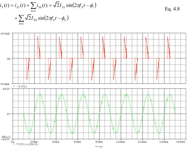
and the power losses decrease. As a consequence, we obtain a smaller sized transformer with the disadvantage of a lower power factor. On the contrary, by reducing the value of the buffer capacitance, the output voltage ripple increases on the buffer, this implies a greater peak current through both the primary of the transformer and the power switch, and the efficiency is reduced. The advantage is to have a higher power factor. As it is shown in Figure 4.6, the line current is heavily distorted. The non-sinusoidal waveform is(t) that is repeated with frequency fs, may be developed in Fourier series and may be expressed as
the sum of its harmonic components. The line current has a dominant fundamental frequency, and contains infinite components with multiple frequencies of the fundamental, which are the distortion components of the current:
(
)
(
h h)
h Sh l S S h Sh S S t f I t f I t i t i t i f p f p -+ -= + =å
å
¹ ¹ 2 sin 2 2 sin 2 ) ( ) ( ) ( 1 1 1 1 Eq. 4.8Figure 4.6: Line current on the top: voltage main on the bottom (fcutoff = 1/10 fsw).
The harmonic components of the current with frequencies above the fundamental do not contribute to the average power (active power) that is supplied from the source with sinusoidal voltage. The power factor (PF) is defined as the ratio between the active power and the apparent power:
( )
( )
l S S S S l S S I I I V I V S P PF = = 1cosf = 1cosf Eq. 4.9The peak amplitudes of the most significant harmonics that are contained in the line current are shown in Figure 4.7. The rms value of the current line (IS) in Eq. 4.9 has been
calculated by taking into account the distortion content till the twentieth harmonic. The line current is(t) is far from a sinusoidal waveform, and the amount of the distortion of the
current waveform is given by the total harmonic distortion (THD) index.
Figure 4.7: Fourier analysis of the line current (fcutoff = 1/10 fsw).
100 100 % , 1 2 , 1 2 , , 1 , rms S rms S rms S rms S rms dis I I I I I THD = = - Eq. 4.10
Analyses at different values of the cut-off frequency of the p filter have been performed, and the performance of the converter was evaluated. The most significant figures are written in Table 4.1. In order to obtain better PF values and lower THD values, a change in the input stage of the flyback converter has been made, as it is shown in Figure 4.8.
Table 4.1
Freq.(fsw) [Hz] DVout [%] Pout [W] Pa [W] S [VA] PF h THD %
1/10 1.2 10.48 13.53 22.92 0.59 0.78 126
1/50 0.2 10.50 13.78 31.54 0.44 0.76 194
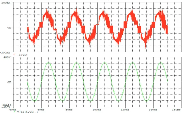
Figure 4.8: Schematic of flyback converter with a valley PFC.
The p input filter was changed with a passive power factor corrector circuit (PFC, or valley circuit), and before the rectifier bridge was introduced a LC filter with a cut-off frequency fixed at about 1/10 of the switching frequency. Subsequently a sensitivity analysis was made in order to evaluate the parameter influence on the input quantities (PF, THD, and efficiency) of the converter. In particular, attention was focused on the output capacitor. The main results are detailed in Table 4.2. The current and voltage waveforms on the main line are shown in Figure 4.9, while the harmonic components of the current are shown in Figure 4.10.
Table 4.2 Cout [µF]
fcutoff
[kHz] Pout [W] Pa [W] S [VA] PF h THD % DVout %
220 11.3 11.7 14.6 16.0 0.91 0.80 32.3 14.7
470 11.3 10.9 13.6 16.5 0.82 0.80 58.3 6.9
Figure 4.9: Line current on the top and voltage main on the bottom (Cout=220 µF).
Figure 4.10: Fourier analysis of the line current (Cout=220 µF).
There are different types of dimming strategies well-known and reported in literature. Such strategies may be summarized into two main categories: analogue dimming and PWM dimming [12] and [13]. The former case requires that the current of the LEDs is regulated in a continuous way; this technique takes the advantage of the linearity between the output luminous flux of the LED and the forward current. The latter case is a bit more complicated, and may be split into different types of PWM dimming. They are based on the principle of driving the diode with a constant peak current, and modulating the duty cycle of the current, by implementing a PWM control current. In this way the current in the diode will be modulated above the critical frequency which causes the flicker effect (>120 Hz), typically the frequency ranges between 200 Hz and 400 Hz.
The technique used to control the brightness in the flyback topology is the PWM series dimming, where a switch (power MOSFET) is connected in series with the LEDs. Another technique is the high frequency PWM series dimming, that has similar features of the above technique, but by means of an appropriate control loop the control of the LED is with equal switching frequency of the converter.
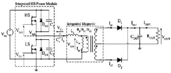
4.2.1.2. Resonant converter
The high-frequency resonant converters allow using capacitor and inductor, respectively used to filter the voltage and current ripple, with small size and small weight [14]. In fact, if compared with converter working in PWM mode, resonant converter technology has a high switching frequency, small switching losses, a wide range of input voltage, high efficiency, light weight, small size, small EMI noise, small switch stress. The schematic for a LED driving circuit is shown in Figure 4.11, where the two switches at the same arm bridge are an integrated module [14] – [17].
Figure 4.11: Resonant circuit schematic for LED.
4.2.2. Non-isolated topology
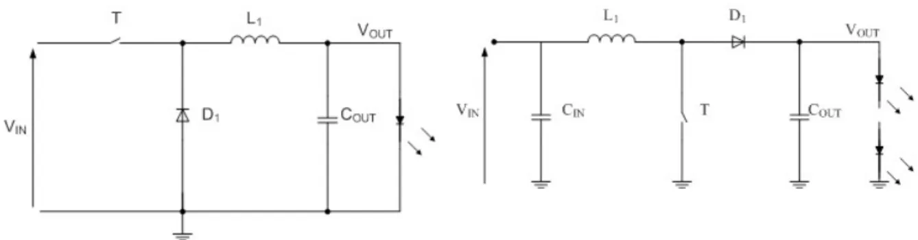
Three main dc-dc switching converters topologies, without isolation, may be used as LED driving circuits: the buck, the boost, and the Z converter (Figure 4.12 to Figure 4.14). These converters are used in order to convert a DC input voltage in to a regulated DC output voltage at a required level.
Figure 4.12: Schematic of the buck converter. Figure 4.13: Boost converter LED driver.
Figure 4.14: Schematic of a Z converter.
4.2.2.1. Buck converter
Solid-state lighting bulbs may be driven in an existing lighting fixture and require a high-voltage step-down ratio in order to produce an output voltage of about 10–20 V. A buck converter provides a low average output voltage lower than the input voltage. The most important advantage is the low number of passive component of the topology and the high efficiency. The structure of a buck circuit is simple, and its design is easy. By changing the duty cycle we can get different output voltages. But in case of small duty cycle, traditional non-isolated step-down pulse width modulation buck converters may suffer of poor efficiency due to the long diode freewheeling time. One other disadvantage is the not easy drive of the power switch, because its reference terminal is floating.
4.2.2.2. Boost converter
A boost converter provides an average output voltage greater than the input voltage. Therefore, boost converters are ideal for LED driver applications where the LED string voltage is greater than the input voltage. The converter can easily be designed to operate at efficiencies greater than 90%. Both the source of the MOSFET and LED string are
connected to a common ground. This simplifies the sensing of the LED current (unlike the buck converter where we have to choose between either a high side MOSFET driver and a high side current sensor). The input current is continuous which makes easy to filter the input ripple current (and easier to meet any required conducted EMI standards). However, boost converters have some disadvantages. The output current of the boost converter is a pulsed waveform. Thus, a large output capacitor is required to reduce the current ripple in the LED.
4.2.2.3. Zeta converter
A new alternative topology has been proposed to drive LED lamps. The proposed circuit shows a very high efficiency beyond keeping constant current through the LED. According to [14], when applying white LEDs for display backlighting or other illumination applications, there are two reasons to drive them with constant current:
1. To avoid violating the absolute maximum current rating, thus compromising the reliability.
2. To obtain predictable and matched luminous intensity and chromaticity from each LED.
It is important to note that a white LED luminous intensity and chromaticity (colour) are tested and best controlled by driving it with constant current. The topology shown in Figure 4.14 is a ZETA converter. According to [12], the circuit has the following properties:
1) The transformerless version of the converter has a positive dc voltage transfer function M, i.e., the circuit is a non-inverting converter.
2) The dc voltage transfer function M can be either less or greater than 1, depending on the value of the switch duty cycle D:
0.5 > D for 1 > M and 0.5 D for 1 M< £ Eq. 4.11
3) The transfer function M is independent of the load resistance RL in the
continuous mode of operation by neglecting the power losses, while it is proportional to the square root of RL in the discontinuous mode of operation.
4) In both the transformerless and with transformer versions of the converter, the entire dc input energy is first converted into ac energy and then the ac energy is converted into the dc output energy.
4.2.3. Analysis of the results
The LED lighting market is an area that is rapidly expanding, and the manufacturers adopt for indoor or outdoor lighting the “retrofit” concept looking to substitute the incandescent bulbs. A power converter able to drive a string of ten diodes is required for a LED lamp having an equivalent luminous flux of a 60 W incandescent lamp. The analysis has been devoted to a flyback converter, and to its sensitivity analysis to the electrical parameter change. In particular, when a p filter is the input of the converter, it was noted that by reducing the value of the buffer capacity an increase of the ripple of output voltage appears. This implies an increased peak of the current through the primary of the transformer and the power switch. The advantage is a higher power factor. In order to improve the PF and THD values a valley PFC circuit is used, but the output voltage ripple increases till 15% of the nominal voltage (30V). The analogue dimming is the simplest one to control the brightness of the LED lamp. although it has disadvantages, because high injection currents may lead to a lack of linearity between injected current and luminous flux output, and a noticeable shift in chromaticity coordinates, which are considered the most important drawback of this technique [18]. Alternatively, PWM techniques may be used and in particular the PWM series dimming. This technique maintains all the advantage and has not the disadvantage of the previous technique; however, this technique can lead to fluctuations of the feedback signal due to the absence of load for long transient. Series high frequency PWM dimming is an appropriate control technique that allows turning the switch in series to the LEDs at the same switching frequency of the power converter, in this way the previous problem of fluctuations is cancelled at the cost of a slight efficiency reduction.
Chapter 5
Analysis of the conventional
techniques to reduce the power
5. Introduction
There are many different type of techniques that allow reducing the waste of energy in a power converter [19] [20].
5.1. Start up circuit
The start up resistor can be replaced by an internal high voltage current source consisting of a J-FET [21]. At start up, the internal high voltage current source supplies the internal bias and charges the external capacitor that is connected to the Vcc pin as it is shown in Figure 5.1. After Vcc is reached, the PWM controller begins switching and the internal high voltage current source is disabled. Thus, the power dissipation in the start-up resistor can be removed.
Figure 5.1: Start-up circuit.
5.2. Switching frequency reduction
A common technique widely used to reduce the power consumption is reducing the switching frequency. The power consumption in a power MOSFET is proportional to the switching frequency and the hysteresis losses in the transformer too. By a frequency reduction switching losses may be reduced, but entering into the human range of hearing may cause a problem. In order to reduce the audible noise, it is required to limit the peak of the drain current when passing through several kHz range. The optimum value of peak drain current is determined by trade-off between efficiency and audible noise.
5.2.1. Effective switching frequency reduction
In general, human ears are most sensitive to frequencies around 2 kHz and less sensitive to frequencies which are higher or lower as shown in Figure 5.2. The Figure is a graphical representation of the sensitivity of the ear to frequencies over the human range of hearing at various loudness levels.
Figure 5.2: Equal Loudness curves.
Each line shows the intensity level for the range of frequency that gives a subjective impression of similar loudness with reference to a starting level of 1 kHz.
In order to limit the current level, the burst operation mode is employed to reduce the fundamental frequency. The fundamental frequency is reduced to several hundred Hz, as shown in Figure 5.3. In standby mode, the functional blocks in PWM controller for normal operation are disabled and therefore the operating current can be reduced minimizing power consumption in the PWM IC.
5.3. Output voltage disconnection
When the output load is disabled in the standby mode, some amount of leakage current always flows in the output side.
Reducing this leakage current requires a whole new design circuit in the secondary side. . In some special cases, output disconnection method is used as shown in Figure 5.4. However, this approach increases the total cost and deteriorates the efficiency.
Figure 5.4: Output voltage disconnection.
5.4. Output voltage drop
Another approach to reducing losses caused by leakage current in the high voltage output is lowering the output voltage in the standby mode [22]. This approach is widely used when the supply for the micro-controller is provided through a linear regulator as shown in Figure 5.5. The range of the output drop is limited by the linear regulator. In order to drop the output voltage much in standby mode, the input voltage of the linear regulator in normal operation should be set as high as possible. However, this results in severe loss in the linear regulator in normal operation.
Figure 5.5: Output voltage drop.
5.5. Output voltage drop with auxiliary winding
As discussed in the previous session, the range of the output drop is limited by the linear regulator input voltage. By using voltage drop approach with auxiliary winding, the output can drop without limitation by the linear regulator supply voltage; Figure 5.6 shows the auxiliary winding circuit for the output voltage drop. Vo1 provides the supply voltage
for the linear regulator in normal operation while Vo2 supplies the linear regulator in
standby mode. Therefore, the linear regulator input voltage is selectively provided by Vo1
and Vo2, minimizing the power dissipation in the linear regulator.
5.6. Auxiliary Power supply
For auxiliary converters in high power applications above 200 W, reducing the switching frequency has limitation in lowering switching losses since MOSFET with a relatively large output capacitance is used. In that case, the use of another auxiliary power supply that is optimized for the standby power level is preferred. In the standby mode, the main power supply is shut down completely.