UNIVERSITÀ DEGLI STUDI DI MESSINA
DIPARTIMENTO DI SCIENZE MATEMATICHE E INFORMATICHE,
SCIENZE FISICHE E SCIENZE DELLA TERRA
Dottorato di Ricerca in Fisica
SSD FIS/04
Characterization of GET Electronics
coupled to the CHIMERA and FARCOS multi-detectors
for nuclear reaction studies
Tesi di:
Saverio De Luca
Tutor:
Prof. Antonio Trifirò
Co-tutor:
Dott. Giuseppe Cardella
Introduction
Studying the equation of state (EoS) of asymmetric nuclear matter rep-resents one of the main goals in nuclear physics research [1]. The EoS is determined by the details of in-medium nuclear interaction and plays a key role in determining the properties of astrophysical objects, such as neutron stars and supernovae explosions [2].
Accessing information on the interaction between neutrons and protons in a dilute and hot environment similar to that existing in stars is however difficult and one is forced to rely on measurements from astrophysical obser-vations and nuclear reactions studied at accelerator facilities. In this kind of reactions, a high number of fragments are produced and it is important to identify them in a wide range of energy, mass and angles.
For this reason in the late 1990s at LNS (Laboratori Nazionali del Sud) of Catania the 4π multi-detector CHIMERA (Charged Heavy Ion Mass and Energy Resolving Array) was designed and constructed [3]. CHIMERA is equipped with electronics in discrete components that, also through analysis in the form of the signal produced by detected particles, allows a recognition of fragments in change and/or mass in a wide dynamic range [4].
This detector is still very powerful. Part of its electronics (for the Silicon stage) has been recently updated, however it needs some further improvement. From the point of view of physics cases, a large number of investigations performed in heavy-ion collision reaserches are now based on two- and multi-particle correlation measurements. These measurements require high angular and energy resolution, especially focused on the detection of light particles abundantly produced during the overall dynamical evolution of excited and dilute nuclear systems produced in central and peripheral impacts. To
im-The present work is devoted to study and characterization of the compact GET electronics, that must be used for both the final FARCOS array, consti-tuted by 20 telescopes (about 2600 detectors) and the 4π CHIMERA CsI(Tl) (1192 detectors) front-end, now obsolete. Our choice was to develop a first stage front-end circuit for FARCOS (including new ASIC pre-amplifiers) and new dual-gain modules coupled to a compact hardware architecture cover-ing digitalization and signal readout, synchronization and trigger functions. These last aspects are covered by the GET project.
With the compact GET electronics we have large advantages respect to old electronics based on discrete components, for example few racks will be enough for all FARCOS and CHIMERA (CsI detectors) electronics and we will use only 5 W for 256 channels, so the total power consumption will be much lower than the present (for CHIMERA we need now about 60 kW of power in 10 racks).
The new electronics is fully digital so allowing the complete storage of the detector signals with obvious advantages for the pulse shape analysis and noise rejection. Moreover, the compactness of this electronics allows us to transport it easily.
The PhD thesis is organized in four chapters.
In chapter 1, first of all it is described the physics cases, with a general introduction to the different “correlation methods”. Then both FARCOS project and the choice of GET electornics are described. After, a comparison between the analog electronics and digital one is made. Finally a description of software filters, that we use for online and offline analysis, is described.
In chapter 2, the construction details of CHIMERA, FARCOS-PROTOTYPE and GET electronics are described. Moreover, the Dual Gain Module (nec-essary for double dynamic range) and identification methods developed by using such electronics are described.
In chapter 3, the results of the performed tests with radioactive sources and with internal and external pulser are described.
Finally, chapter 4 is devoted to results obtained during on beams experi-ment are reported. A final paragraph reports the perspectives using the new electronics.
1 Physics cases and experimental techniques 1
1.1 Physics cases . . . 1
1.2 FARCOS project . . . 5
1.3 Digital acquisition: advantages and disadvantages . . . 7
1.4 Software filters . . . 9
2 Experimental set-up 11 2.1 CHIMERA . . . 11
2.1.1 Basic detection module . . . 15
2.2 Electronic chain . . . 16
2.2.1 The electronic chain of Silicon detectors . . . 17
2.2.2 The electronic chain of CsI(Tl) crystals . . . 19
2.3 FARCOS . . . 19
2.3.1 Main characteristics of the FARCOS array . . . 20
2.3.2 Detector: the CsI(Tl) stage . . . 21
2.3.3 Positioning system of FARCOS telescopes . . . 22
2.4 GET electronics . . . 24
2.5 The Dual Gain Module . . . 28
2.6 Identification techniques . . . 30
2.6.1 ∆E-E technique . . . 31
2.6.2 E-RiseTime technique . . . 32
2.6.3 E-RiseTime for Silicon detectors . . . 34
CONTENTS
3 Tests with pulser and sources 38
3.1 New Data acquisition for FARCOS and CHIMERA . . . 38
3.2 Set-up of GET electronics . . . 41
3.3 Linearity of the system and noise . . . 44
3.4 Multiplicity threshold . . . 48
3.5 Tests with α-source and γ-rays on FARCOS and CHIMERA CsI scintillators . . . 51
3.6 Tests with α-source on strip detectors . . . 55
3.7 Tests with high-purity Germanium (HPGe) detector . . . 56
3.8 Characterization of software filters developed to determine the signal amplitude . . . 59
3.9 Tests on time resolution . . . 67
3.10 Dead time measurements . . . 70
4 Tests of GET electronics with experimental beams 71 4.1 Test with7Li beam . . . 71
4.2 Test with 62 MeV proton beam . . . 73
4.3 Test of GET electronics in CLIR experiment . . . 75
4.4 GET-CHI test . . . 81
4.5 BARRIERS Experiment . . . 87
Physics cases and
experimental techniques
1.1
Physics cases
In heavy-ion collisions at intermediate energies (from 20 to 200 AM eV ) the nuclei are exposed to a violent collective compression phase where the overlapping nuclear matter is predicted to reach values of density well above the saturation value ρ0 = 0.17 nucleon/f m3.
The following expansion phase brings the density down to significant low values, the so-called freeze-out phase (ρ ∼ 0.3 ρ0), which turns up in the
multi-fragmentation phase where many excited clusters and light particles are ejected from the collision center.
Figure 1.1: Representation of the time evolution of a heavy-ion collision with highlighted the different reaction phases. To give an idea of the time scale of the process, the freeze-out phase (fragment ejection) occurs some 10−22s after the beginning of the collision.
1.1. PHYSICS CASES
Figure 1.1 shows a representation of the time evolution of a heavy-ion collision, highlighting the different reaction phases. If on one side, there is still not the certainty whether the system schieves full equilibrium in the freeze-out phase, on the other there are clear evidences of the presence of secondary decays from emitted fragments.
This complex scenario can be investigated with the powerful techniques of intensity interferometry and correlation functions [5]. Correlation functions at small relative momentum allow measurements of the order of magnitude of 10−15m for spatial dimensions and of 10−23÷ 10−20s for time intervals [6]. Despite this great achievement, one of the fundamental problems is to disentangle the prompt emitting sources from secondary emitting ones whose characteristic time scales are order of magnitude greater.
The difficulty is even magnified by the extrem sensitivity to parameters such as beam energy, the centrality of the collision (impact parameter) and the mass of the system [5]. Nevertheless, a suitable gating of impact parameters, reaction plane, charged particle multiplicity and other global parameters comes in partial aid to decipher the several emitting source components [7]. Proton-proton correlation function is the most common technique exploited in Hanbury-Brown-Twiss (HBT) intensity interferometry studies. It is defined as follow
Y12( ~p1, ~p2) = c12· (1 + R~p(~q))Y1( ~p1)Y2( ~p2) (1.1)
where Y12( ~p1, ~p2) is the yield of the two coincident particles detected at the
same event, C12 is a normalization constant obtained by imposing R~p(~q) = 0
for very large value of relative momentum ~q of the particles, Y1( ~p1) and
Y2( ~p2) are the yields of the single particles, ~p is the total momentum of the
pair and 1 + R~p(~q) is the proton-proton correlation function.
Thanks to the anti-symmetrization of the two-body wave function, the shape of the correlation function can be related to the different emission time delay between the protons. This is formally stated in the Koonin-Pratt (KP) equation
1 + R~p(~q) = 1 +
Z
Sp~(~r) · K(~q, ~r) · d~r (1.2)
where 1 + Rp~(~q) is the two-proton correlation function, S~p(~r) is the
with a relative distance ~r measured at the time when the second particle is emitted, K(~q, ~r) is the kernel function and it contains the whole information about the final-state interaction between the two coincident protons, includ-ing their quantum statistics.
Since the correlation function is measured and the kernel function is well known for protons, solving equation 1.2 means extracting the source function, which retains the information on the space-time properties of the particle-emitting sources.
This can be achieved through different approaches, namely Model Sources approaches, Shape-Analysis approaches and Transport Model approaches. The first assumes a specific function underlying the shape of the correlation function. The second realeases such arbitrary assumption and numerically invert the equation. The Imaging technique is the most known and used method that belong to this group. The third compares the measured function to numerically computed models and allows probing transport properties such as nucleon-nucleon collision cross-section and the density dependence of the symmetry energy.
As an example, in Figure 1.2 (left panel) we show a set of proton-proton cor-relation functions, each of them corresponding to a different total momentum gating, for the reaction14N + 197Au at 75 MeV per nucleon. The dashed lines are computed assuming Gaussian-shaped source function. Figure 1.2 (right panel) shows the corresponding source functions computed with the
1.1. PHYSICS CASES
Figure 1.2: Example of proton-proton (left panel) correlation function for the reaction 14N + 197Au at 75 MeV per nucleon. Each curve derives from a different total momentum gating. The dashed lines are computed assuming Gaussian-shaped source function. Right panel: corresponding source functions computed with the imaging techniques [7].
It is worth noticing that the order of magnitude of the spatial resolution is the fm. Since during heavy-ion collisions at intermediate energies a large variety of particles and fragments are produced, it is necessary to extend the application of the correlation function methods to the Light Charged Particles (LCP) and Intermediate Mass Fragment (IMF) other than protons. The complex scenario that emerges from these studies, consequence of the complex structure of LCPs and IMF, calls for higher-resolution detection systems in order to be properly addressed. Correlation functions with LCPs are at the basis of the emission time and chronology assessment for the particle-emitting sources, the understanding of which would facilitate the comprehension on primary fragments production mechanisms in heavy-ion collisions. IMF-IMF correlation functions are another important subject of study since they allow the extraction of the space-time properties of the nuclear system produced during the reaction at the time of their freeze-out stage. This gives a unique eye on multi-fragmentation phenomena and their
possible link to a liquid-gas phase transition in nuclear matter.
Two-nucleon correlation is also a precious tool to investigate the isospin dependence of the nuclear equation of state, which is perhaps the most uncertain property of neutron-rich matter.
The correlation function concept can be extended to a multi-particle scenario to explore the spectroscopic properties of the unbound states produced during the evolution of the nuclear system that follows the collision. This technique, called Multi-Particle Correlation Spectroscopy (MPCS), is a powerful tool since it allows disentangling simultaneous decays from sequential decays processes and gives access to characterization of the short-living exotic nuclei [7, 8].
Finally correlation measurements and the study of direct reactions in inverse kinematics with stable and radioactive ion beams (RIBs) push toward the measurements of momentum vector and of its correlation that imposes high energy and angular resolution. In addition two-or many-particle correlation measurements require large statistics that can be gained widening the solid angular coverage. The conflicting quest of performing correlation measure-ments of LCPs and IMFs or of joint detection of the emitted light particle and the residual heavy fragment arising from the stripping occurred in the incoming RIB in the study of direct reactions in inverse kinematics requires a wide dynamic range of the detector front-end electronics system. Moreover, the low energy foreseen for the RIB at SPES and SPIRAL2 requires low identification thresholds for both LCPs and IMFs, and the study of the correlation of LCPs even at high energies imposes a high stopping power. Last but not least, the geometry has to be as simple and versatile as possible to allow modular assembling and easy coupling with other detectors like spectrometers, neutron detectors and 4π arrays e. g. CHIMERA.
1.2
FARCOS project
The FARCOS (Femtoscope ARray for COrrelations and Spectroscopy) project is a detectors system with high pixelation capabilities in order to perform high precision measurements of two- and multi-particle correlations. It consists of a new array that is designed and constructed inside the
INFN-1.2. FARCOS PROJECT
NEWCHIM experiment. The original idea, driving the construction of the prototype of FARCOS during the years 2010 − 2014 [9], has been developed inside of the CHIMERA/EXOCHIM collaboration with researchers and tech-nical staff from the INFN-Sezione of Catania, Milano and Napoli, Laboratori Nazionali del Sud, University of Catania, Milano and Napoli, and including the participation of researchers from France, Spain and USA. An example of a configuration of FARCOS array is illustrated in Figure 1.3:
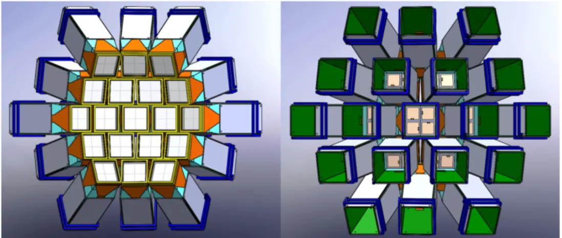
Figure 1.3: A possible configuration of FARCOS array, front view (left panel) and back view (right panel). Courtesy of C. Serrano and L. Acosta. For more details see chapter 2.
FARCOS will be a compact and relatively large-solid angle detection system, characterized by both high angular and energy resolution, modularity and having the peculiarity to be movable in a rather simple way in order to be coupled to different detector systems in laboratories around the world. In fact, it will be possible to use FARCOS not only coupled to CHIMERA detector [5], but also with others existing and under developing devices (as for example INDRA [10], GARFIELD [11], FAZIA [12], MUST2 [13]). Farcos must be designed to be able to cover different angular regions, depending on the physics case to be addressed, and on the beam energy and kinematics of the reaction. FARCOS array can be also used in coincidence with focal detection planes of magnetic spectrometers (as for example MAGNEX [14], PRISMA [15], VAMOS [16]). This can represent important progresses not only for typical studies on isospin physics, already covered in the framework
of the CHIMERA experiments [2], but also in studies of heavy-ion collisions, where two- and multi-particle correlations play a fundamental role in both dynamics and spectroscopy.
In summary, new perspectives will be opened in nuclear physics with both stable and radioactive beams working with the CHIMERA-FARCOS system at INFN-LNS, or coupling FARCOS with other detectors in national and international laboratories (as for example SPES - LNL, GANIL, GSI). In particular, the FARCOS array is thought mainly to be used in the studies of correlations between charged particles in reactions at low and intermediate energies, as well as, in spectroscopic studies and in the raising investigations in the already mentioned femtoscopy studies, in order to extract information about the space-time properties of nuclear reactions. Recent advances in analysis techniques based on fitting or inversion procedures (as for example the imaging method) have allowed to get valuable information on the size (volume, density) of particle emitting sources produced during heavy-ion collisions, as well as their lifetimes [ 17]. Typically, these measurements are performed with devoted arrays of silicon and scintillator crystals covering a specific portion of the accessible phase space in the reaction. Then, the availability of powerful 4π detector, allows getting a unique tool to characterize the whole collision event in terms of impact parameter, reaction plane, collective motion and to extract important information about the dynamic and timescale of fragment emission [18].
1.3
Digital acquisition: advantages and
disadvan-tages
Regarding the electronics for the FARCOS project, the first detector tests of the FARCOS prototype were performed by using the standard CHIMERA Front End electronics. In particular, due to the availability of the recent (2008) upgrading electronics for Silicon Pulse shape, we decided to use part of it. However because this electronics is too expensive, take too much space, need high power supply and consequently efficient cooling systems not always available, we decided to search for a new compact electronics
1.3. DIGITAL ACQUISITION: ADVANTAGES AND DISADVANTAGES
with good enough characteristics and reasonably low cost. After various test, the final choice was to design new ASIC preamplifiers for Silicon strips (developed at INFN and Politecnico of Milano), and to read and digitize the signals from such preamplifiers using the GET electronics recently designed for Time Projection Chamber (TPC) applications. Nevertheless, adapter boards must be developed in order to interface such ASIC preamplifiers with GET to match our needs of large dynamic range of the digital converters. CAEN(I)-Power supply are chosen for the bias of all the channels.
The foreseen number of channels for the FARCOS system when comprising 20 telescopes will be 2560 channels. This number of channels is large enough to discourage the use of SMD electronics of conventional SMD electronics. On the other hand, this number is too low to justify large efforts of dedicated man power for the development and adoption of a full VLSI readout electronics from the front-end to the back-end. In view of the main requirement of FARCOS, i.e., the flexibility and adaptability, especially due to the different envisaged physical cases, it is more reasonable taking into account for the available man power-expertise and budget constraints to develop a dedicated front-end while exploiting available solutions that can be customized thanks to the re-configurability offered by FPGAs systems for the back-end. Besides the already mentioned advantages, digital electronics allows us to obtain other ones. For example, an advantage of the digital acquisition is the fact that pedestal is measured event by event (by measuring the baseline of the preamplifier signal) and can be simply subtracted.
Moreover with digital acquisition the signal shape is completely saved/stored, allowing us to vary offline the parameters used in the software filters in order to improve resolution and ratio of signal/noise.
Obviously we have to pay a price for all such advantages. In this case, the price is that one need a very large disk storage space available in order to save the complete trace of the signals. Moreover, the transmission bandwidth of ACQ system must be very large to be able to transfer from the readout electronics to the storage farm the full amount of data to be processed. Finally yet importantly, we need a very large CPU-power for the on-line and off-line computer farms in order to check the progress of the experiment and to do the complete data analysis. These aspects will be better analyzed in
the following.
1.4
Software filters
Digital FIR (Finite Impulse Response) filters are applied in our signal processing analysis to the signals after baseline restorer. The way to obtain a digital filter is to define a convolution of the input signal sj with the digital
filters “response function” rk of finite duration M :
(r ∗ s)j = M 2 X k=−M2+1 sj−krk (1.3)
The digital filter is called finite when the response function is different from zero in the interval −M2 < k ≤ M2 and zero otherwise, where M is an even integer number. When the impulse response is used in this way it is also called “filter kernel” because can be easily pre-calculated for a given response function in a window with a number of discrete points equal to M (we shall define in the following the number of samples M as number of “taps”). In our signal processing for the GET acquisition we have mostly often used the so-called “triangular filter” (see Figure 1.4) [19].
Figure 1.4: Response function that we used (Triangular filter) in comparison with other kind of filters (Kaiser, Rectangular, Hanning and Hamming).
1.4. SOFTWARE FILTERS
The response function R(k) is approximated, using a symmetric triangle, in a window defined as:
R(k) = (
1 +2kM if − M−12 ≤ k < 0 1 −2kM if 0 ≤ k ≤ M−12 .
The number of M points used is strictly dependent from the kind of calculation we want to perform on the original signal. For example, in the calculation of a rise-time, filters with a low number of taps are used (or no filter at all) in order to avoid signal distorsions, while filters with a big number of taps are more suitable for the evaluation of the signal maximum amplitude.
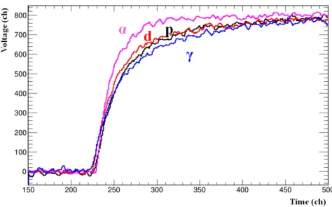
In Figure 1.5 we show the results of application of the triangular filter to determine the rise-time (blue lines with 17 taps used) and the signal amplitude (green lines with 251 taps used) for digitalized waveforms of a Silicon detector and of a CsI(Tl) scintillator (red lines).
Figure 1.5: Digitized waveforms (red lines in both panels) of a Silicon detector (left panel) and of a SI(Tl) scintillator (right panel), digitally filtered signals used to determine the signal amplitude (green lines in both panels) and filtered signals used to determinate the rise-time (blue lines in both panels).
As shown in Figure 1.5, using triangular filters is a good compromise because we obtain good results saving, at same time, the CPU machine time in the online analysis because the calculation is relatively fast (depending on the number of the filter taps).
Experimental set-up
2.1
CHIMERA
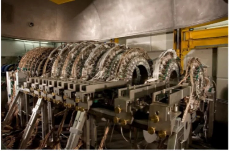
CHIMERA (Charged Heavy Ion Mass and Energy Resolving Array) is a 4π multi-detector designed to study heavy-ion collisions in the intermediate and low Energy range. It can be schematically described as a set of 1192 detection cells arranged in 35 rings following a cylindrical geometry along the beam axis. The whole apparatus has a total length of about 4 m, as illustrated in Figure 2.1, and it is setup in a vacuum chamber.
2.1. CHIMERA
The basic detection module of CHIMERA is a telescope made of a Silicon detector (Si), followed by a Cesium Iodide Thallium activated scintillation detector (CsI(Tl)), coupled to a photodiode Figure 2.2.
Figure 2.2: The basic detection module of CHIMERA apparatus. The mechanical structure can be essentially divided into two differently shaped blocks: the forward one (see Figure 2.3), covering the polar angles between 1◦ and 30◦, is made of 688 modules assembled in 18 rings, grouped in couples, and supported by 9 wheels centered on the beam axis. The rings of telescopes are placed at a distance from the target varying from 350 to 100 cm, with increasing polar angle. Each wheel is divided into 16, 24, 32, 40 or 48 trapezoidal cells, depending on its polar coordinate, containing each one a detection module, or telescope.
The remaining angular range, between 30◦ and 176◦, is instead covered by the sphere of 40 cm internal radius (see Figure 2.4).
Figure 2.4: Photo of the sphere of the CHIMERA multi-detector. Whose 15 forward (according to the beam direction) rings are segmented into 32 cells while the two most backward ones are segmented into 16 and 8 cells respectively. Each module of this spherical structure consists in a steel box containing the Cesium Iodide crystal with the Silicon detector placed at its front end. The large number of telescopes and the geometrical config-uration give to CHIMERA a high granularity, thus reducing the multi-hit probability, and a high solid angle coverage, about 94 % of 4π. All these features, in addiction to low energy detection threshold, give the possibility to have a complete event reconstruction.
2.1. CHIMERA
Figure 2.5: Geometrical characteristics of the CHIMERA array. For each detector in a ring, the distance from target, minimum and maximum polar angle, azimuthal angle range and covered solid angle are specified.
2.1.1 Basic detection module
Each module of CHIMERA is composed by two-detection stage: the first one is a 300 µm thick Silicon detector. As well known, Silicon is a very widely used material for particle detectors, because of its good energy resolution, its high density (2.33 g/cm3), the low energy needed to create an electron-hole pair (3.6 eV with respect to 30 eV in gases), its fast signal collection (about 10 ns in 300 µm of thickness for light particles) and its good time resolution. In particular, the Silicon detectors used in CHIMERA have a trapezoidal shape and were made by using the planar technology [20]. With this technique, it is possible to have well defined detector thickness, very sharp active zones (the p+ layer inactive area is 500 A thick), and◦ extremely thin and homogeneous junction thickness. These Silicon detectors have a geometry that changes according to the position in the device. In the forward part of the apparatus, each cell contains two telescopes, and thus two Silicon detectors (internal and external detectors in the same pad) characterized by the presence of two active zones that work independently of one another.
Both the active zones are surrounded by a guard ring located 50 µm away in the dead zone (due to the planar technology) of the edge of the detector. The 504 Si detectors of the sphere instead are simple pad detectors; even in this case a 500 µm dead zone, in which a guard ring is placed, surrounds the active area. A schematic representation of wheels and sphere Silicon detector is shown in Figure 2.6:
2.2. ELECTRONIC CHAIN
The second stage of CHIMERA’s telescope consists of Cesium Iodide Thallium activated crystals CsI(Tl); these scintillators are used to measure the residual energy of particles that punch through the Silicon detector [21]. This kind of crystals are chosen as second stage detectors because of their high density, so that their high stopping power allows to reduce the thickness needed to stop high energy charged particles and fragments. Moreover CsI(Tl) scintillators are characterized by relatively low cost, simple handling, a good resistance to radiation damage and external factors, good light output performance when coupled with a photodiode or a photomultiplier, and offer the possibility to make an isotopic identification. In fact the light versus time shape of the output signal from the scintillator, consist of a fast component and a slow one whose decay constants depend on the specific energy loss of incident fragments, and therefore on their energy, charge and mass [22]. A disadvantage of these scintillators is the non-linearity (at low energies) in light response that is therefore not directly proportional to deposited energy, depending on the nuclear species of the fragment and on its ionizing power. The shape of CHIMERA’s crystals is a truncated pyramid with a trapezoidal base; the dimensions of the front surfaces are the same of the Silicon detectors and depend on the position in the device. The backward surface is bigger than the front one, depending on the thickness of the crystal that ranges from 3 to 12 cm.
Finally, the CsI(Tl) crystals are coupled with photodiodes (PD), preferred to photomultipliers mostly for their low operating voltage (so low power dissipation), their simple handling and compact assembly under vacuum. The used photodiodes, manufactured by Hamamatsu Photonics, are 300 µm thick with an active surface of 18 × 18 mm2 and are located into a ceramic support with the front side (corresponding to the light entrance hole) protected by a thin window of transparent epoxy resin.
2.2
Electronic chain
Two different electronic chains handle the signals coming from Silicon detectors and photodiodes; these chains process and digitize signals read by the acquisition system. In a typical experiment performed by means of
CHIMERA apparatus it is necessary that electronics satisfy some require-ments such as a large dynamic range (from M eV to GeV ), a low power dissipation under vacuum, a good timing in order to reach a resolution of about 1 % in velocity measurements through the TOF technique [23], a good energy resolution and high level of flexibility in coupling the detector with other experimental devices. With the aim to reduce electronic noise and signal losses in parasitic circuits, which strongly affect the energy resolution, the preamplifiers (PA) of Silicon detectors and photodiodes are placed on a motherboard inside the vacuum chamber. The motherboards for the de-tectors of the forward part are located on the external surface of the wheels and contain four PAs: two for the internal telescope and two for the external one, since each telescope needs two PAs, one for the Silicon detector and the other for the photodiode. On the other hand, the motherboards in the sphere have only two preamplifiers, corresponding to only one telescope, and they are located on the top of the metallic baskets containing telescopes. All the motherboards are cooled for stability of the electronics. The voltage generators for detectors and preamplifiers with the rest of electronic chain are placed outside the vacuum chamber.
2.2.1 The electronic chain of Silicon detectors
The recently upgraded basic electronic chain of Silicon detectors is shown in Figure 2.7:
2.2. ELECTRONIC CHAIN
Figure 2.7: The basic front-end electronics of Silicon detectors.
A charge preamplifier (designed to reach good timing measurements with high capacitance detector) provides a first amplification of signals; it integrates the signal of the detector giving an output independent of detector capacity and proportional to the charge produced by detected particles. In order to control electronic stability, each preamplifier is provided with a test input, which accepts signals coming from a pulse generator. The output is a single negative fast signal carrying time and energy information, character-ized by a rise-time from 10 to 200 ns and a decay time of about 200 µs. The preamplifier sensitivity changes with the polar angle: in the most forward part (θ = 1◦÷10◦), where the more energetic particles are expected, the sensitivity
is 2 mV /M eV , while at larger angles (θ = 10◦÷ 176◦) it is 4.5 mV /M eV . Then the output signal is processed by the amplifiers (pulse shape) channels model N1568, produced by CAEN. Such compact modules are particularly studied to measure the rise-time of the Silicon signal, enabling us to get the charge of particles stopped in the first detection stage [ 24]. In order to measure the rise-time of Silicon signals, each channel is equipped with two different discriminators, characterized by different constant fraction (30 % and 80 %). These two CFDs process two copies of the same timing signal
and send their output signals to two different TDCs; each TDC, working in common stop mode, measure the time from the start signal given by the pulse shape module, and the stop signal generated using the cyclotron phase. The time measured by the T30 % channel is used for time of flight evaluation, while the difference between T30 % and T80 % TDCs is used to evaluate the
signal rise-time.
The pulse shape module is also equipped with a stretcher that prepare the en-ergy signal to be integrated in a simple way by a Charge-to-Digital Converter (QDC). The QDC is able to perform a double charge encoding: the High Gain (HG) and the Low Gain (LG) coding. In the first case, an amplification factor 8× is applied in order to obtain a good energy resolution also for low Energy signals. The module can also produce a chainable multiplicity signal. This signal has a level of 25 mV for each fired channel in the chain, and it is used for the event trigger.
Detailed information about general architecture of CHIMERA Data Acquisi-tion System can be found in [25]-[30].
2.2.2 The electronic chain of CsI(Tl) crystals
The old electronics for the CsI line is going to be replaced because it is based on amplifiers SILENA not more in production since more than 10 years. We will not discuss the details of such old electronics because it will be replaced by the GET one. In the GET chapter some examples will be given of the different results obtained using the two electronics. Only the preamplifier under vacuum will be maintained. The signal coming from the CsI(Tl) (coupled with a photodiode) detector firstly is processed by a charge preamplifier that presents the same characteristics of those used for Si detectors, except for the sensitivity that is of the order of 50 ÷ 100 mV /M eV . The rise-time of output signals is significantly longer than 50 ns because of the scintillation light characteristics.
2.3
FARCOS
The following paragraphs are devoted to describe the FARCOS (Fem-toscope ARray for COrrelations and Spectroscopy) project, aimed at the
2.3. FARCOS
development of a detection system with high pixelation capabilities in order to perform high precision measurements.
2.3.1 Main characteristics of the FARCOS array
FARCOS has been conceived as a compact high resolution array; the basic telescope consists of two DSSD (Double-sided Silicon Strip Detector) 300 µm thick and 1500 µm thick, as first and second stage respectively. The third stage is constituted by 4 CsI(Tl) crystals; each of them has a length of 60 mm and a sensitive area of 32 × 32 mm2, arranged in square configuration 2 × 2. Each crystal produces a scintillation light collected by Silicon photodiodes 300 µm thick with an area of 18 × 18 mm2. The total detection area of Silicon detectors is 64 × 64 mm2, adapted to cover the total area of the four CsI(Tl) crystals placed behind. The scheme of the three stages of one FARCOS cluster is shown in Figure 2.8:
Figure 2.8: Schematic representation of a FARCOS module.
Each DSSD features 32 horizontal and 32 vertical strips providing 1024 equivalent pixels of 2 × 2 mm2. This segmentation allows to reconstruct the impact position of detected particles, hence their emission angles, with high resolution. High angular resolution combined with high energy resolution provide a good measurement of relative energy and momentum vector. The
performance of FARCOS allows one to detect particles in a wide dynamic range going from MeV to GeV; the high stopping power of thick CsI(Tl) allows indeed to stop high energy light particles, while low thresholds for particle identification will be attained with pulse shape techniques applied to the first DSSD [31].
2.3.2 Detector: the CsI(Tl) stage
The final configuration of the FARCOS CsI(Tl) detector is a truncated pyramidal shape with the square basis of the backward face (where photodiode is mounted) of the order of 38 × 38 mm2 and a front face of 32 × 32 mm2. This shape ensures that particles impinging on the second and 31st strip of the second stage Silicon detector are correctly stopped inside the CsI(Tl). While particles impinging on the first and 32nd strips can escape from CsI(tl) before being completely stopped when the telescope is placed at a distance of 25 cm (distance of the second Silicon stage) from the target. This choice moreover was performed in order to limit the size of telescopes, allowing a more compact mounting if different detection distance are needed. On the other hand, because of the finite size of Silicon strips, some typical known problems arise for the good definition of the effective solid angle of the first and last strips in matching the two silicon stages. However, the more external strips generally suffer of a larger noise (with respect to the internal ones) and are often excluded from the analysis, so, it is very important to save data coming from the second and 31st strips. This truncated pyramidal shape has also the advantage to allow a more sure mounting of CsI(Tl). With this shape in fact, the crystal cannot be pushed from the back (wedge effect), so saving for accidental touches of the bonding of the back side of Silicon strip detector. Obviously this means that the global size of telescopes (taking into account also electronic boards) will be larger than the one of Silicon strips (including package the side of front surface becomes 72 mm) and it will produce a slightly smaller efficiency in the coverage of solid angle, more important when detector will be mounted far from the target. Nevertheless this is a relatively good compromise between the solid angle coverage and detector performances.
2.3. FARCOS
2.3.3 Positioning system of FARCOS telescopes
In order to perform high precision measurements of two- and multi-particle correlations it is necessary to determine with high accuracy the absolute angular position of every pixel with respect to the beam line. The system we have developed is based on a laser source placed at 0◦, 5 m after the target position for mounting inside the CHIMERA chamber. The laser beam, characterized by a diameter of 0.8 mm and a divergence of 1.0 mrad, will be directed on a mirror placed in the target position, and reflected towards the detector, as shown in Figure 2.9:
Figure 2.9: Outline of the laser beamline designed for the exact positioning of every telescope.
The laser beam moreover will be pulsed in short bunches, in order to produce a detectable signal on the fired strip of the first DSSD. The mirror will be mounted on a scanning Galvo system [32] (see Figure 2.10) which will rotate it around a horizontal axis with angular resolution of 0.01◦.
Figure 2.10: Galvo system used to rotate the mirror placed in the position of the target.
The Galvo system will be installed on the target support, which will rotate the galvo system around the vertical axis with angular resolution of 0.01◦. After a suitable calibration this system can ensure the positioning of telescopes with adequate precision; the main error we could make is produced by a displacement of the mirror located in the target position. Using a converging lens placed before the mirror, laser beam will be focused on several reference points chosen on every telescope.
Figure 2.11: Reflecting system of the laser beam positioned in CHIMERA vacuum chamber during various tests at LNS.
2.4. GET ELECTRONICS
2.4
GET electronics
In the last decade the development of more and more powerful digital devices, the availability of fast relatively low cost storage devices, and the improvement of data transmission speed, due to optic fiber technology, allowed the development of new fully digital data acquisition systems. As already mentioned, in such data acquisitions the complete shape of the signal can be stored. This is a big advantage because the signal treatment can be changed and adapted to any different experimental condition. Sophisticated software filter can be applied to clean signal from noise. The pedestal can be measured event by event, largely improving resolution. Pulse shape analysis of the detector signal can be applied, improving particle identification capabilities, but also allowing to clean pile up events. Last, but not least, very sophisticated filter can also be optimized to extract more precise timing information. One of the last developed ACQ SYSTEM of such kind is the GET one. This electronics was developed, in the last years, with the aim to produce a low cost and very flexible electronics for the new generation of TPC under construction in the world. Many laboratories joined their efforts to build such new electronics (Saclay, Ganil, Bordeaux, MSU, RIKEN), and nowadays it is adopted or tested by more than 20 new detector system in constructions around the world. The flexibility of such electronics was fully shown by the fact that many detector system that now are going to use it are different than TPC.
GET eletronics is based on AGET asic chip [33] (Asic for General Electronics for Tpc) circuit (see Figure 2.12) produced by CEA laboratory at Saclay.
Figure 2.12: Schematic representation of GET electronics.
Four of these chips are soldered on the ASAD (Asic Support and Analog-Digital conversion) card with four 12-bit ADC (one per AGET). Each AGET handles up to 64 channels (256 inputs for ASAD). The digital outputs of the 4 ADCs are transmitted with a maximum speed of 1.2 Gbit/s to the CoBo board. The CoBo (Concentration Board) manages up to 4 ASAD, so using 4 CoBo we are able to manage more than 4000 detectors. The CoBo board is responsible for applying a time stamp, zero suppression and compression algorithms to the data. It will also serve as a communication intermediary between the Asad and the outside world with a maximum speed of 1 Gbit/s per CoBo. The MUTANT (MUltiplicity Trigger ANd Time) card manages the multiplicity, conditions for the trigger, and the distribution of the clock on the whole system. It also allows conversation with other acquisition systems by transferring/receiving external triggers. The global data are transmitted through network switch to a computer farm with a maximum speed of 10 Gbit/s for storage and online analysis.
The CoBos and the trigger (MUTANT) modules are housed in a µTCA (Micro Communications Computing Architecture) crate that can host up to 11 CoBos and 1 trigger module. It implements a serial backplane bus and
2.4. GET ELECTRONICS
a network Ethernet infractructure built into the system. We have adopted the Vadatech VT893 µTCA crate [34] that is already validated to operate with the GET electronics. Through the TCA Ethernet switch the CoBo(s) can exchange data up to 10 Gb/s with an external computers farm for data analysis and storage.
The main characteristics of GET electronics is flexibility and programmability of the system. One can easily change gain, adjust the time scale to cope with timing of the detector, adapt the trigger system not only using the information on channel multiplicity but also on the position of fired channel. A single channel in its standard version integrates mainly: a charge sensitive preamplifier, an analogue filter (shaper), a discriminator for trigger building and a 512-sample analog memory (SCA) (see Figure 2.13).
Figure 2.13: Scheme of a single channel of the AGET chip.
The analog filter is formed by Pole Zero Cancellation stage followed by a 2-complex pole Sallen-Key low pass filter. The peaking time of the global filter is selectable among several values (16 values) in the range of 70 ns to 1 µs. The filtered signal is sent to the analogic memory and discriminator inputs.
512 cell-depth circular buffer is used, in which the analogic signal coming out from the shaper is continuously sampled and stored. The sampling frequency can be set from 1 MHz to 100 MHz. The sampler is stopped on a trigger decision. In the read out phase, the analogue data are multiplexed in time domain toward a single output and sent to the external 12-bit ADC at the readout frequency range of 25 MHz . In the nominal mode, the input signal goes through the input of the CSA (Charge Sensitive Amplifier). By slow control, it is possible to switch the signal to the input of SKfilter or inverting 2× Gain just before the SCA. In this case, the internal supply of the CSA and PZC filter is cut off.
Part of the SCA noise will be probably coherent between channels; to perform common mode noise rejection, 4 extra channels named FPN (Fixed Pattern Noise) are included in the chip. FPN channels are treated by the SCA exactly as the other channels. Offline, their outputs can be subtracted to the 64 analog channels. This pseudo-differential operation is supposed to reject the major part of the coherent noise due to 2× Gain of Gain2 and SCA such as clock feed-through and couplings through the substrate. It also improves the power supplies rejection ratio (PSRR) of the chip.
These channels are distributed uniformly in the chip and their readout in-dexes are: 11, 22, 45 and 56. To reduce the amount of data and dead time, we decided to enable only a FPN (channel 11) for each AGET subtracting it to the other 64 analog channels. As already mentioned a FARCOS telescope is constituted by 2 DSSD 32×32 strips and 4 CsI(Tl) detectors with photodiode readout. To save electronics it was decided to use back strips only for one DSSD (the first or the second stage depending on physics case). Moreover, double dynamics is fundamental in the case of front strips while it is less important for the back side that is not characterized by very good resolution. So we need two electronic channels for each front strip and only 32 channels for the back strips. The double dynamics is also necessary for the CsI(Tl), therefore we need 8 more electronic channels for each telescope. In summary for each telescope we need 128 electronic channels for the front strips, 32 channels for the back strips and 8 for the CsI(Tl). For the 20 telescopes we therefore need 10 ASAD cards for front strips, 3 ASAD cards for the back strips (one half filled), and 1 ASAD card for CsI(Tl) (with only 160
2.5. THE DUAL GAIN MODULE
channels filled). We cannot mix back strips electronics and CsI(Tl) because they need a different treatment of signals. 100 MHz sampling frequency is in fact required for silicon signals while 50 or probably better 25 MHz is required for CsI(Tl) signals.
We will not use the preamplifier input of AGET chips. During the tests we have seen that one can very well use either the SKfilter input, if the signals had some noisy in order to improve resolution or directly the Gain2 input when this is not necessary. Depending on the physics case, one has also to take into account that in SKfilter mode one has a factor ×2 gain; therefore, the maximum energy of the allowed dynamic range is consequently reduced. GET electronics will be used for the CsI(Tl) of CHIMERA and for all FARCOS.
To read 14 ASAD cards one needs at least 4 CoBo cards. Notice that by using more CoBo cards it is possible to reduce the total dead time; in fact by reducing the number of channel read through each CoBo, one will have a larger band width for each channel in the transfer trough Ethernet to the PC farm dedicated to the on-line analysis and data storage.
One MUTANT board is clearly required to manage the trigger, the synchro-nization of all CoBo cards among them and of the GET ACQ with the other ACQs needed for the detector systems to be coupled to FARCOS.
2.5
The Dual Gain Module
As described in previous paragraph, for some of the channels of FARCOS and for CHIMERA CsI we need to implement Double dynamical range. We therefore had to develop some adapter cards, slightly different for CHIMERA and FARCOS that will do:
1. the conversion from differential to single-ended signaling (only for FARCOS);
2. the splitting of signals for the case of detector front strip for FARCOS and for CHIMERA CsI;
3. independent gain adjustment for the two series of splitted signals, with possibility to have selectable gains 18, 14, 12, 1, 2, 4, 8;
4. signal level adapter (AGET chips works better if signals have a positive baseline from 0.5 to 2 V ).
We need therefore to develop three different interface cards. A DUAL gain module for FARCOS (with differential input) a DUAL GAIN for CHIMERA (with single ended input) and single gain with level adapter for back strip of FARCOS. Because the philosophy of the different cards is similar we will describe here the dual gain module for CHIMERA.
The Dual Gain Module is a multichannel digitally programmable gain ampli-fier (PGA). The module split each FARCOS/CHIMERA channel and adjust the signals level to the ASAD input dynamic range. The Dual Gain Module will be developed with a form-factor as the one used for the ASAD board (VME) in order to optimize the connection between the two boards. In this configuration, each ASAD card will be connected to two Dual Gain Modules. The detail of the set-up is shown in Figure 2.14:
Figure 2.14: ASAD card and Dual Gain Module connection diagram. To prevent the output signal from swinging outside the common-mode input range of the ASAD card each PGA channel provides both high and low output clamp protection. In addition, the PGA allows the output signal baseline setup. The Dual Gain Module is based on a microcontrollers system
2.6. IDENTIFICATION TECHNIQUES
that will take care of the module slow-control, the parameters setting and the user communication through a dedicated communication bus.
The electronics consumer device used to amplify or attenuate the signal consists of a separate low-noise input preamplifier and a programmable gain amplifier. To evaluate and test the PGA performances some beta-cards were developed and results of the test are described later in this work.
The input impedance of every channel is 50 Ω while the output impedance can be 50 Ω for long cable transmission systems or high impedance (10 KΩ typically) for short cable. The user can digitally set the gain in the range from 0.032 V /V to 4 V /V (from −30 dB to 12 dB) at 50 Ω output impedance. Moreover one can double the gain range using high impedance load.
2.6
Identification techniques
During our tests on GET electronics we have used various methods to identify particles in charge and/or mass. In this paragraph we will give some generalities about the used identification techniques. More details will be given in next chapters with many examples. The energy measurement is based on the physical process by which a charged particle loses part of its (or the whole) energy when crosses a material. The identification methods
until now adopted are three:
1. ∆E-E technique, using the signals coming from the Silicon and the CsI(Tl) detectors, is employed for charge identification of heavier ions, and charge and mass identification of the lighter ones;
2. E-RiseTime, obtained by signals coming out from the CsI(Tl) detectors. Test were also performed with silicon signals;
3. Pulse shape discrimination technique, using the fast and slow component of signals, can be also used to identify the light charged particles; this method was used with the previous CsI(Tl) electronics allowing isotopic separation for energetic particles with Z ≤ 4 stopped in the CsI(Tl) scintillator. It can be also used with GET as was shown in previous test with other digital acquisitions [35].
The effective identification limits depend on atomic number, mass and energy of detected particle, and on the position of the detector.
2.6.1 ∆E-E technique
Thanks to the use of telescopes constituted by combination of two or more detectors, it is possible to identify in charge and mass the particles through the ∆E-E technique. Due to inelastic collisions with atomic electrons and ionization of the target nuclei, a charged particle that crosses a material layer loses energy. The average energy lost per unit path, called “stopping power” (indicated by the symbol dEdx) depends on charge, mass and energy of the incident particle, according to the following approximation of the Bethe-Block formula:
dE dx ∝
AZ2
E (2.1)
where A, Z and E correspond to the atomic mass number, the atomic number and the kinetic energy of the incident particle respectively. If the particle, in our case the reaction fragment, is energetic enough to punch through the Silicon detector with thickness, and if the detector response goes linearly with the deposited energy, the output signal has an amplitude proportional to:
dE ∝ dE
dx∆x (2.2)
then, if the incident particle is stopped in the scintillator, the output fast component signal from this last stage of the telescope is proportional to residual energy just released in Cesium, Eres. The sum of these quantities
gives the total kinetic energy of the particle:
E = ∆Esi+ Eres(CsI) (2.3)
combining the two quantities in equation 2.2 and equation 2.3 several groups of hyperbole’s branches are noticeable in a ∆E-E scatter plot: each group corresponds to a Z value and, inside it, each branch corresponds to a different isotope of the same element. Often however ∆E-Eres(CsI) are also used for
such identification bidimensional histogram neglecting ∆Esi in equation 2.3
2.6. IDENTIFICATION TECHNIQUES
Figure 2.15: Bidimensional histogram obtained with16O beam at 55 AM eV and using GET electronics, isotopic resolution can be seen for Be ions.
2.6.2 E-RiseTime technique
This technique consists in determining the rise-time (from 20 % to 80 %) for the digital signal. This is done using a software triangular filter (which we will discuss in the next chapter) with a given number of taps (the number of nodes can be changed off-line to improve the identification of the detected particles in CsI(Tl) scintillators). A rise-time analysis was performed with quite good results as shown in Figure 2.16. As for the ∆E-E method, also in this case each group corresponds to a Z value and, inside it, each branch corresponds to a different isotope of the same element (see Figure 2.16).
Figure 2.16: Example of Energy (Y) vs Rise-time (X) bidimensional histogram obtained with fragmentantion beam on CH2 at 62 MeV. In this case, GET
electronics was used at 50 MHz of sampling frequency.
To better understand the possibility of this identification method one can plot signals of different particles detected with equal energy. A selection of such signals is plotted in Figure 2.17:
2.6. IDENTIFICATION TECHNIQUES
Figure 2.17: Collection of traces for different particles releasing the same light on CsI(Tl). The much faster light collection with α particles respect to deuterons, protons and γ-rays (or light elementary particles such as µ and π) can be well seen.
2.6.3 E-RiseTime for Silicon detectors
In Chimera we use the analog PSD with the method of two discriminators to measure the rise-time of particles stopped in Silicon detector and from this extract the particle charge (see paragraph 2.2.1). During the test performed with GET electronics it was not possible to have experiments with many particles stopped in Silicon detectors in order to check the feasibility of a similar method. However we performed a test, using a not depleted Silicon detector. In this way the electric field inside the detector is very low determined only by the junction, and the charge collection time is therefore very slow. The particle identification capability became very good, even if energy resolution is lost. In Figure 2.18 we show the result of this test.
Figure 2.18: Example of Energy in Silicon detector (Y) vs Rise-time (X) bidimensional histogram obtained with fragmentantion beam on CH2 at 62
MeV.
We note the beautiful charge identification obtained. We therefore conclude that GET electronics will be very good also for the measurement of charge of particles stopped in Silicon detectors via the method of pulse shape analysis of Silicon signal.
2.6.4 Fast-slow technique
The Pulse Shape Discrimination (PSD) technique is used in CHIMERA in order to identify particles stopped in the scintillator1; for high energy light particle, according to equation 2.1, ∆E signal becomes negligible thus it is not possible to use ∆E-E method. These particle are identified by means of the light signals collected by the photodiodes and sent into the relative electronic chain. In fact, the CsI(Tl) crystal, when excited by an incident particle, produces light mainly in two different types of physical processes,
1
From 2008 the pulse shape technique was implemented also for the Silicon detectors, allowing the charge identification of less energetic particles that stop inside the first detection stage. Since the early 60s, it is well known that signal produce by ionizing particles detected in Silicon depends on both atomic mass A and atomic number Z of the particles [36, 37]
2.6. IDENTIFICATION TECHNIQUES
resulting in two distinct light output components, commonly named fast and slow, reflecting energy deposited by the particle in the crystal, and also the particle species. Fast and slow components are characterized by two different decay constants, τf and τs respectively. Such constants govern
the temporal evolution of emission process, so that the output signal from CsI(Tl) is described by the combination of the two exponential components in the following expression:
V (t) = V1e −t τf + V 2e− t τs (2.4)
where V (t) is the the light pulse amplitude at time t, V1 and V2 are the light
amplitudes for the fast and slow components at time t = 0. The amplitude V1 increases with increasing of stopping power dEdx of incident particles, so
depending on their energy, charge and mass, while V2 the is less sensitive to
the incident particle species. This property of the CsI(Tl) crystal is the base of the pulse shape analysis.
Figure 2.19: An example of integration of fast and slow components. In Figure 2.19 we illustrate a case of fast and slow components of a signal. Knowing the combination of the two yields contained in the fast and slow
components it is possible to infer species and energy of the impinging particle. Another advantage of digital acquisition is the possibility of changing and/or move the gates of fast and slow components of signals to optimize the particle identifications.
However, the pulse shape analysis is not peculiar of CsI and Silicon detector but is quite a general technique and can be applied to other kind of detectors; we have also used this method during the Barriers experiment for the signals coming out from a Plastic scintillator.
Chapter 3
Tests with pulser and sources
3.1
New Data acquisition for FARCOS and CHIMERA
The data acquisition system (DAQ) for FARCOS takes into account the adoption of the GET project digital electronics described in the previous chapter. In addition, it allows for the coupling with the DAQ of CHIMERA 4π detector; beside it is thought to be flexible enough in order to be coupled with other possible existing DAQ system by assuming minor changes. Indeed, a part of CHIMERA itself (for CsI(Tl) detectors) will adopt the GET front-end electronics as main readout system. On the other hand the electronic and readout front-end (FEE) for Silicon (Si) detectors in CHIMERA (more recently upgraded for Si pulse-shape analysis [2, 38]) will stay bound to the current electronic chain that has, as final element, the analog codifiers (QDCs, Charge to Digital Converters and TDCs, Time to Digital Converter) housed in a VME bus. As a general rule, the data acquisition system for FARCOS allows for:
1. standalone readout for FARCOS detectors;
2. coupling the CHIMERA readout standard analogic (Silicon detectors) and digital acquisition (CsI(Tl) scintillators);
3. an easy coupling with others external devices (including CHIMERA). This is done using a standardized frame buffer encapsulating the event data together with the basic information needed to merge the event data with
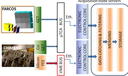
DAQ information coming from other devices (time-stamping and/or event numbering).The main task of data acquisition is to link the data flow coming from the front-end electronic (Readout) with the data Storage (see Figure 3.1).
Figure 3.1: Schematic view of CHIMERA and FARCOS DAQ coupling. See text for details.
Intermediate tasks are data filtering, data analysis and on-line monitoring; these three last tasks are essential steps. They are crucial in particular for digital data acquisition where on-line pulse shape analysis (PSA) has to be applied to the digital samples in order to process the physical information from signals (energy, rise-time, time-of-flight, gated scintillators light compo-nents, etc). Final tasks are the merging of all the data belonging to the same event (event building) and data storing. Our choice in order to manage all these tasks is to use a hardware computing infrastructure (a farm of servers) where a distributed data acquisition framework NARVAL [39], developed at IPN Orsay, handles data flow and processes them among the different tasks described before. In this contest both the CHIMERA data readout and the GET one will be supervised and coordinated by the NARVAL system. NARVAL is a modular, reconfigurable and distributed object oriented soft-ware for data acquisition, transport and filtering. It can coordinate different acquisitions as well handle the data flow through different acquisition tasks. The term “distributed” means that the tasks can run in one core of a specific
3.1. NEW DATA ACQUISITION FOR FARCOS AND CHIMERA
computer or in different computers of a computing farm using a CORBA equivalent inter-process communication.
Figure 3.2: Simplified pictorial example of a NARVAL topology view for a setup with 2 CoBo(s) running with the GET Electronics and a VME data acquisition (CHIMERA). A topology is configured in NARVAL by defining a corresponding file in XML format.
The basic concept of NARVAL is the “actor”. An actor handles buffered flow of data. It is an object class that can be interfaced with a specific code written in ADA95 or C++ producing a shared library. Figure 3.2 shows an example of a realistic topology when the coupling of GET and CHIMERA DAQ is envisaged. The Electronic Control Core (ECC) is the interface with the hardware for control and monitoring (for example in the initialization phase), communicating setup data and acquisition commands by means of Web services like the one defined by the SOAP protocol [40] using a client-server technology. For CHIMERA DAQ this new software component has of course to be implemented from scratch (CHIMERA SOAP Server) while it is already running for GET electronics. The actors called “catcher” collect the event data and distribute them for other tasks. The
intermediate actors (“watcher”) send data to clients computers for example for PSA data analysis of the digitized sample or the spectra monitoring. The event builder (“merger”) is an actor that collects data belonging to the same events on the basis of the time-stamp, the event number or both. The final task, in the example of Figure 3.1, is the data storage of the merged events. The Run Control Core (RCC) handles and coordinates all the common data acquisition activity and the status of the system. This is not part of the NARVAL software. In our tests with the GET electronics and NARVAL we have chosen to adapt to our needs the Run Control Core software developed at GANIL laboratory [41]. Together with the adoption of the NARVAL framework, this makes easier the planning of project for future common experiments with GANIL and other laboratories involving FARCOS and, in particular, it fulfils the main characteristic of FARCOS as a “highly transportable” detector array [6].
3.2
Set-up of GET electronics
As has often been said, GET is a fully digital electronics. This new device is able to manage thousands of electronic channels by remote control. As for any complex ACQ system, one must set many parameters to adapt the set-up to a particular experiment. In order to perform this task a program is available in the GET software package get-config-wizard.
In Figure 3.3 an example of use of this program is shown. In particular, we see some parameters needed to configure the CoBo modules. These parameters are applied to the all ASAD cards connected to the CoBo. For example, the “WritingClockFrequency”, that can be set from 12 , 5 MHz to 100 MHz, indicates the sampling frequency of the ASAD cards. For this reason we can use some CoBo for Silicon detectors (with 100 MHz sampling frequency) and some CoBo (with 25−50 MHz sampling frequency) for CsI(Tl) scintillators. Another important parameter is the “TriggerDelay”. We set this parameter so that the start of the signals is from channel 100 on the x-axis. This is important because we use the first 100 channels for subtracting the pedestal to signals. When the “triggerMode” is “onMultlipicity” it means that we are triggering on the multiplicity of the events. Threshold is
3.2. SET-UP OF GET ELECTRONICS
settable with “multiplicityThreshold” parameter. To change the time period in which two or more events detected in different channels can be considered simultaneously we have to set the “moltWindowSize”. This parameter sets the width (number of samples) of the multiplicity window (in units of 40 ns). For low multiplicity, for example if it is lower than 10, it can be ok to use a value of 1. Finally with “Generator” we active and set the internal pulser. With the ASAD[*] simultaneously all ASAD cards connected can be set, although, clearly, the setting of each ASAD can be changed individually, acting on ASAD[0] or ASAD[1] and so on. The same considerations are applicable at Aget and channel levels, as shown in Figure 3.4.
Figure 3.3: Screen of some parameters of a CoBo, settable by remote control.
Figure 3.4 shows parameters at Aget and channel levels. At the Aget level, when the “TestModeSellection” parameter is on “nothing”, the input
Figure 3.4: Screen of some parameters at Aget and channel levels, settable by remote control.
signal (in this case for the Aget[0]) is sent to: 1. CSA input if “ExternalLink” is on “none”;
2. SKfilter input if “ExternalLink” is on “SKfilterinput”; 3. ADC if “ExternalLink” is on “Gain-2 input”.
For tests with internal pulser “TestModeSellection” parameter must be on “functionality” and “ExternalLink” must be on “none”. The “peackingTime”
parameter sets the characteristic of the internal pulser and the shaping time of SKfilter stage. It is, as just seen, settable with 16 values from 70 ns to 1014 ns.
3.3. LINEARITY OF THE SYSTEM AND NOISE
polarity bit). This value is set by 2 internal programmable DACs. The 4 bits of the first one “GlobalThresholdValue”, common to the 64 channels, define the 3 MSB (Most Significant Bits) of the threshold value and the polarity of the input signal. The second DAC is attached to the channel and defines the 4 LSB (Less Significant Bits) of the threshold value.
At the channel level we can see, in Figure 3.4, the “Triggerinhibition” pa-rameter that can be on:
1. “inhibit trigger” if we want exclude the channel by the trigger; 2. “inhibit channel” if we want exclude the channel (it is important to
note that for a more stable multiplicity trigger a relatively large number of channels should be enabled to trigger);
3. “none” if we want the channel on and that it takes part to the trigger. The “Gain” and “zeroSuppressionThreshold” will be not used in our case. Another important parameter is “Reading”. It allows us to read the channel “always”, “never” and “only if it”. In this last case the channel is active but it storage the digitalized signal only if the amplitude signal exceeds the noise threshold. This option is important to reduce the transferred data and dead time.
To optimize GET acquisition we worked mostly on these parameters. To increase the ratio signal/noise we often adopted the SKfilter input. In this input stage, we used a peacking time of 1014 ns for very noisy signals and peacking time of 502 ns and minor ones for less noisy signals. However in case we do not want to perturb too much the original rise-time of the signal, a small peaking time should be used.
3.3
Linearity of the system and noise
In order to check the linearity and measure the noise threshold, we first did some preliminary test with internal and external pulser. We performed these tests using one ASAD card read by a reduced CoBo (see Figure 3.5) (test device based on a ML507 evaluation board of virtex5 FPGA).
Figure 3.5: The test system with one ASAD card and the Reduced CoBo.
The linearity (see Figure 3.6) and noise were compared to similar mea-surements performed using a 12 bit oscilloscope LECROY. We used the “Gain2” input in the AGET chip so directly converting the preamplifier signal
without any filtering.
Figure 3.6: Linearity response of ASAD card.
The non-linearity measured is less than 1 % between 10 % and 90 % of the scale, being larger only at small values of the signals, where quantization errors probably influence such measurement. One has to note that the good linearity of the system allows us to calibrate the device with few points when we will transport the GET electronics in other laboratories. We
3.3. LINEARITY OF THE SYSTEM AND NOISE
also compared the RMS noise, measured with the oscilloscope, with the standard deviation value of the peak measured with the GET electronics (see Figure 3.7). The behaviors observed are rather similar and compatible with calibration. We note that the higher noise measured for the largest value of the pulser amplitude seems more due to a saturation problem of the used set-up. Therefore, we have verified that the noise doesnt depend on the GET electronics.
Figure 3.7: Noise measurements performed by oscilloscope (left panel) and Get electronics (right panel).
We performed other test, to verify thresholds behaviour, using both internal and external pulsers. The pulser signal, generated in the chip, is sent to the charge sensitive preamplifier (CSA) of the channel, then to the SKfilter, after to the memory based on a Switched Capacitor Array structure (SCA) and finally, if the signal is larger than the noise threshold, it is sent to ADC (one for each AGET).
We performed tests using 50 MHz sampling frequency on an AGET with only few activated input channels. We obtained a linear dependence between the discriminator threshold (in channels) and the pulse height necessary to trigger the system, as shown in Figure 3.8: