Graphene-based derivative as interfacial layer in graphene/n-Si Schottky barrier solar cells
Andrea Gnisci1*, Giuliana Faggio1, Giacomo Messina1, Laura Lancellotti2, Eugenia Bobeico2, Paola Delli Veneri2, Andrea Capasso3, Theodoros Dikonimos4, Nicola Lisi41 Department of Information Engineering, Infrastructures, and Sustainable Energy, University “Mediterranea” of Reggio Calabria, Reggio Calabria 89124, Italyn
2 ENEA, Portici Research Center, Portici, Naples 80055, Italy
3 Department of Materials Science and Engineering, Yonsei University, Seoul 03722, Republic of Korea 4 ENEA, DTE PCU IPSE, Casaccia Research Centre, Rome 00123, Italy
Corresponding Author Email: [email protected] https://doi.org/10.18280/ama_a.550307
Received: 19 March 2018 Accepted: 22 May 2018
ABSTRACT
In Schottky barrier solar cell (SBSC), the interface between absorber and front electrode plays a vital role for reducing the dark current, blocking the majority carriers injected into the electrode at forward bias, reducing surface recombination and passivating the silicon surface. In this respect, the addition of interfacial layer between the semiconductor absorber and the metal electrode can reflect into an improvement of the device performance. Here we combine n-type crystalline silicon with stacks of graphene and graphene-based derivative (GBD) layers with different properties, in order to realize efficient SBSCs. Graphene layers with different structure, work function and electrical conductivity, were obtained by varying the chemical vapor deposition (CVD) parameters: conductive graphene films were grown at 1070 °C, GBD interfacial layers at 790 °C. The stacked structures were fabricated by the multiple transfer of these films. The films and the stacks were characterized by Raman spectroscopy. The device with the GBD interlayer (acting as hole transport layer) exhibits promising performances in terms of external quantum efficiency (EQE) and power conversion efficiency (PCE, ~5 %). Doping treatments with nitric acid vapor was performed and improved the cell PCE up to 6.7 %.
Keywords:
CVD graphene, graphene-based derivative, photovoltaics, Raman spectroscopy, solar cell
1. INTRODUCTION
In the last few years, a great deal of interest has been focused on the graphene-on-silicon (Gr/Si) Schottky barrier solar cell cells (SBSC) [1–3]. The recent progress has shown the potential to produce low cost and high efficiency solar cells with this configuration. In Gr/n-Si SBSC the graphene not only serves as a transparent conductive electrode but also contributes as an active layer for carrier separation and hole transport [4–8]. The Gr/n-Si solar cells can be fabricated by simply transferring a graphene film onto a n-Si substrate at room temperature. Their fabrication is thus much less expensive and easier in comparison to traditional Si solar cells based on p-n junctions. The first Gr/n-Si solar cell achieved a power conversion efficiency (PCE) of 1.5 % [4], but within five years this value reached 15.6 % [9], thanks to various improvements, such as graphene’s chemical doping [10–14], the use of multilayered graphene films [15-16], the application of antireflection coatings or light-trapping layers [12-13, 17– 19], and the engineering of the Gr/n-Si interface [9, 20–22]. Among these various approaches, the chemical doping has been considered the most effective method to enhance the performance of Gr/n-Si solar cells. For instance, it has been reported that the PCEs of Gr/n-Si solar cells were improved to
~9 % after doping the graphene films by
bis(trifluoromethanesulfonyl)amide (TFSA) [10] and nitric acid (HNO3) [17-18]. The PCE of a HNO3-doped Gr/n-Si solar cell can increase if combined with the application of an antireflective coating [17, 18]. Nevertheless, the PCE of these
cells are still much lower than that of state-of-the-art crystalline Si solar cells. The performance of Gr/n-Si SBSC is highly affected by the recombination of the charge carriers at the interface due to a low Gr/n-Si Schottky barrier height (SBH) (~0.6–0.7 eV), much smaller than the traditional silicon solar cells, which causes a large leakage current and thus a low open circuit voltage (Voc) [1]. Among the different approaches to reduce charge recombination and improve the performance of Gr/n-Si SBSC, one method consists in engineering the interface between graphene and Si by adding interfacial layers. Such layers can play a key role in suppressing the charge recombination at the interface and improving the Voc of the cell. A high PCE (15.6 %) for Gr/n-Si SBSC has been achieved by optimizing the thickness of the native oxide interfacial layer [9]. The thin native oxide layer (~2 nm) acts as a passivation layer, reducing the influence of surface defects and the reverse dark saturation current, thus improving the Voc. To address this issue, it was proposed to insert an insulating layer between graphene and Si, thereby forming a metal-insulator semiconductor (MIS) structure [6]. In such MIS configuration, the additional insulating layer works as an electron blocking layer preventing the diffusion of electrons (majority carriers) from n-Si to graphene and thus reducing the carrier recombination. An appropriate band alignment between the insulating layer and the n-Si is also required to reduce the effect of hole (minority carrier) transport from n-Si to graphene. Furthermore, the insulating layer should be very thin (down to atomic thickness) and uniform to avoid increasing the series resistance (Rs). SBSC with optimized
Advances in Modelling and Analysis A
Vol. 55, No. 3, September, 2018, pp. 144-150 Journal homepage: http://iieta.org/Journals/AMA/AMA_A
aluminum oxide (Al2O3) [23] or hafnium oxide (HfO2) [24] interfacial layers have been reported to achieve stable, high-efficiency Gr/n-Si junction. It has been reported that the introduction of graphene oxide (GO) [20, 25] or organic polymer film [12, 26] at the Gr/n-Si interface could effectively suppress the interface recombination of Gr/n-Si solar cells and increase the VOC. 2D materials such as MoS2 monolayer [21, 27] and hexagonal boron nitride (h-BN) [28] have been also investigated as effective electron-blocking/hole-transporting layers.
In the present work, we report on the use of a graphene based derivate (GBD) as interlayer, realized by chemical vapor deposition (CVD) of ethanol on copper. Such as the top graphene electrodes, the GBD interlayers are transferred onto silicon at room temperature, thus at lower temperature than the conventional insulating SiOx layers. We characterized graphene films with different structural and electrical properties. SBSC with varying number of graphene and GBD layers were fabricated by using cyclododecane-assisted transfer [29-30], as shown previously for Gr/n-Si SBSC [17] and organic solar cells [31].
SBSC with single and double GBD interlayers were tested and the results have been compared with a standard SBSC without interfacial layers. Single-interlayer Schottky junction showed an increase of SBH and a decrease of Rs and ideality constant (η), confirming the improvements of junction reducing the recombination sites at the interface. A molecular doping treatment (by nitric acid vapors) was performed on the solar cells with single interlayer. The effects of graphene molecular doping on Gr/GBD/n-Si heterojunction solar cell performances have been investigated. After the treatment, the cell’s PCE increased from 4.8 % to 6.7 %.
2. EXPERIMENTAL SECTION 2.1 Sample preparation
Conductive graphene (few layer graphene or thin graphite) and GBD interlayer were grown by ethanol CVD onto the copper substrates respectively at 1070 °C and 790 °C, using the CVD parameters reported in previous works [31-32]. The CVD reactor consists of a cold-wall chamber, made of a quartz tube equipped with an inductively coupled graphite susceptor heater (Figure 1). The heater is excited by a 3 kW (maximum power) radio frequency current source, which is modulated by the signal of a thermocouple buried inside the graphite susceptor. This system presents various advantages over classic CVD configurations: it does not entail the heating of the quartz tube and/or the entire CVD system [33], it allows controlled and fast heating and start-up time for the whole system and the possibility to reach higher temperatures than with more conventional, coaxial quartz tube furnaces.
Figure 1. The inductively heated CVD reactor
Figure 2. Schematic illustration of the 1L-SBSC
After growth, both kind of layers were transferred onto the cell substrates and after each transfer the cell was heated for 60 min at 60°C to help cyclododecane removal, and then to 90°C for 20 min for final drying. Different SBSCs were fabricated with stacks of two or more layers, with graphene as electrode and GBD as interlayer between graphene and n-silicon. The same transfer procedure was applied for transferring each layer onto target substrates for characterizations. For the solar cell fabrication, polished Si substrates ([100]-oriented, n-doped, 1 Ω cm), with thermally grown SiO2 layer (300 nm) were patterned by photolithography and wet-etching of the oxide (by hydrofluoric acid solution) to prepare square windows with an active area of 0.09 cm2. The scheme of the solar cell is shown in Figure 2. The front and back contacts were realized by evaporating Ti/Au on the SiO2 and a Ti/Pd/Ag trilayer on the back side of the n-Si, respectively [17]. The GBD was interposed between conductive graphene and silicon to work as an interlayer in the Schottky junction. The GBD covered the active area, but it was removed from the Au/Ti front electrode; instead, the top graphene layer entirely covered the Au electrode. Two kinds of SBSC devices were fabricated with different top architecture: 1) layer GBD between single-layer graphene and n-Si (1L-SBSC), and 2) double-single-layer GBD between double-layer graphene and n-Si (2L-SBSC). SBSCs based on standard Gr/n-Si junction were also fabricated for comparison. Molecular doping was performed by exposing the top part of the cell to HNO3 vapor (from a 70 % solution diluted 1:1 in deionized water) at ambient conditions for 3 min. Details of the doping process can be found in ref. [34].
2.2 Sample characterization
The sheet resistance of the graphene was measured by four-point probe (NNPSON RESISTAGE RG-8) method in Van der Pauw configuration. Raman spectra were acquired on graphene and GBD films after the transfer onto Si/SiO2 substrates. Raman scattering measurements were carried out at room temperature with a HORIBA Scientific LabRAM HR Evolution Raman spectrometer with an integrated Olympus BX41 microscope. Laser excitation wavelength of 532 nm (2.33 eV) was focused on the sample surface using a 100× objective with a spot size of approximately 1 μm. Low laser power (below 1 mW) was used which minimized sample heating and possible damages. The solar cells were characterized by means of external quantum efficiency (EQE) and current density–voltage (J-V) measurements. EQE measurements were carried out with a Bentham PVE300 apparatus (Reading, U.K.) calibrated with a Si detector and using a probe light with a spot size much smaller than the cell area.
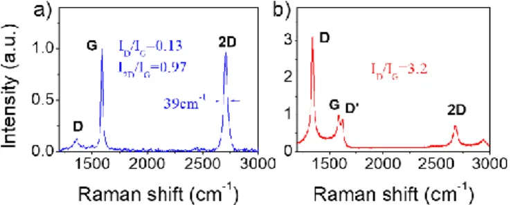
Figure 3. Raman spectra acquired on each layer of the solar cell: a) conductive graphene, b) GBD interlayer
Illuminated J-V characteristics were performed with a Keithley 228a voltage/current source (Keithley Instruments Inc., Cleveland, USA) and HP 3478A multimeter measure unit (Palo Alto, USA). White light illumination was provided by a class AAA solar simulator from WACOM (model WXS- 155S-L2) equipped with a 1000 W Xenon lamp and a 400 W Halogen lamp. The light intensity was calibrated using a mono-Si reference cell in standard test conditions (25° C, AM1.5G, 1000 W/m2).
3. RESULTS AND DISCUSSION
3.1 Structural characterization of graphene and GBD layers
Raman spectra of the graphene and GBD interlayer are reported in Figure 3. The Raman spectrum of graphene (Figure 3a) exhibits the characteristic D, G and 2D peaks respectively at ∼1350 cm−1, ∼1580 cm−1, ∼2700 cm−1 [35]. Commonly the D to G (ID/IG) and 2D to G (I2D/IG) intensity ratios provide quantitative information on defect density and thickness of graphene, respectively [32, 36]. I2D/IG < 1 and ID/IG∼ 0.13 measured values indicate the formation of multilayer graphene [35, 37] with low defect density [38]. The Raman spectrum of the GBD is shown in Figure 3b. The main features of a graphene spectrum are still present, but in this case the D peak strongly intensifies and the defect-related D’ peak at ∼ 1620 cm−1 appears [31]. The high value of ID/IG intensity ratio (∼ 3.2) is typical of defective carbonaceous film [37]. A similar very sharp D peak was already observed in functionalized graphene [39], and in hydrogenated graphene grown at 650° C by plasma-CVD [40]. The sheet resistance of the graphene and GBD films are 0.5 and 124 kΩ/sq, respectively [31]. The charge separation and transport in the 1L-SBSC can be understood from the energy band diagram in Figure 4.
Figure 4. Schematics of band diagrams for 1L-SBSC
For the GBD interlayer, the valance band maximum is 4.9 eV and the absorption in the UV leads to an estimated optical gap of ~ 5.1 eV (as reported in previous work using the same GBD for organic solar cells [31]), while n-Si has the conduction band minimum and valence band maximum of 4.05 and 5.17 eV, respectively. Upon irradiation, electron−hole pairs generated in Si would diffuse across GBD/n-Si interface and then be separated by the built-in electric field of the heterojunction.
3.2 Solar cell characterization
Electrons in the Si conduction band are preferentially collected by the Ti/Pd/Ag electrode (cathode), while injection of electrons from Si to graphene anode is prevented by the interlayer due to the offset between the two conduction bands. On the other hand, holes are readily injected into the valance band of interlayer because of the negligible offset between the two valence bands, and then collected by the graphene anode. Therefore, the interlayer not only acts as the hole transport layer, but also serves as an electron blocking layer for reducing the carrier recombination at the anode. This should lead to a lower saturation current density and hence a larger open circuit voltage for the device.
Devices with single and double GBD interlayers were tested. Figure 5a shows the dark ln(J)-V characteristic of 1L- and 2L-SBSC compared to SBSC. The reverse saturation current density of SBSC is estimated to be 8.9 × 10⁻⁴ mA/cm2 while for 1L-SBSC it decreases to 4 × 10⁻⁴ mA/cm2. An increase to 3.8 × 10⁻³ mA/cm2 is measured in the 2L-SBSC.This hints that the carrier recombination is reduced with the introduction of single GBD layer. On the contrary, the increase of 2L-SBSC reverse saturation current density would indicate the presence of a large quantity of trap states between stack interfaces. The SBH can be evaluate by analyzing the dark J-V characteristic. The diode characteristics of Schottky junction is described by thermionic emission theory of majority carriers over the Schottky barrier according to equation [10]
𝐽 = 𝐽𝑠[exp ( 𝑞𝑉
𝜂𝑘𝐵𝑇) − 1] (1) where η is the ideality factor, kB is Boltzmann’s constant (k=8.62×10⁻⁵ eV/K), T is the temperature in Kelvin, q is the electronic charge (1.6 × 10⁻¹⁹ C) and the saturation current density Js is described by the equation
𝐽𝑠= 𝐴∗𝑇2𝑒𝑥𝑝 (−𝑞(𝑆𝐵𝐻)
𝑘𝐵𝑇 ) (2)
where A* is the effective Richardson constant.
Solar cell SBHs, evaluated by taking the slope at the forward bias linear region of ln(J)-V curve (Figure 5a), are summarized in Table 1. The non-linearity observed in the lower bias part of the forward curve of 2L-SBSC is due to the presence of leakage currents. Such current components are usually attributed to generation and recombination of carriers in the charge space region, field emission and thermionic field emission or surface/edge effects that may lead to local barrier lowering [41, 42]. The η was also extracted from ln(J)-V curve and it is found that it is reduced from 2.15 to 1.6 when a single layer of GBD is inserted in the junction, but it reaches 3.5 value in 2L-SBSC.
Figure 5. (a) Dark ln(J)-V characteristics and (b) Plots of dV/dln(I) versus I for SBSC (blue), 1L-SBSC (red) and
2L-SBSC (black curve)
Typical values for η in undoped graphene/n-Si diodes are in the 1.6-2.0 range [10]. The properties of the junction are strongly affected by unwanted contaminants or defects due to the fabrication process, which acts as charge traps and add interface states. These defects and contaminants cause charge accumulation and induction of charge puddles in graphene, resulting in local variation of the SBH. The spatial inhomogeneity of the barrier contribute to the high η [43]. Accordingly, the high values of the measured ideality constants are associated with the existence of impurities on the graphene and on the GBD layers that are unintentionally formed during the fabrication process and which give rise to associated Schottky barrier inhomogeneities. Only for 1L-SBSC η decreases and this reveals a lower interface recombination and hence better junction quality. Figure 5b shows 𝑑𝑉/𝑑(ln𝐼)versus I plot, from
𝑑𝑉 𝑑(𝑙𝑛 𝐼)=
𝜂𝑘𝐵𝑇
𝑞 + 𝑅𝑠𝐼 (3)
and then it is possible to extract the Rs value from the slope of the curve linear fitting [44]. As also reported in Table 1, Rs is reduced from 216 Ω to 178 Ω for 1L-SBSC, and to 110 Ω for 2L-SBSC.
Table 1. The diode characteristics of Schottky junctions reported in Figure 5 Device SBH(eV) η Rs (Ω) SBSC 0.78 2.15 216 1L-SBSC 0.87 1.60 178 2L-SBSC 0.70 3.50 110 Figure 6. EQE curves without and with OB of SBSC (blue),
1L-SBSC (red) and 2L-SBSC (black)
Additional characterization is presented in Figure 6, which shows the EQE of the SBSCs acquired with and without optical bias (OB). Without OB all devices showed an EQE ~60 % in the wavelength range 650 nm < λ < 800 nm (Figure 6, inset), a value in line with the state of the art of Si solar cells [10]. The EQE curves acquired with OB result unchanged in the case of 1L-SBSC, indicating a significant electron-hole pair generation, separation and collection by the corresponding electrodes. On the other end, the EQE reduction in OB condition observed in the case of SBSC and of 2L-SBSC, indicates an activation of recombination centers responsible for the entrapment of photogenerated carriers. Since the photogeneration for the device without and with the interlayer is identical, the higher EQE observed for the 1L-SBSC with OB is due to more efficient charge separation and charge collection as a result of increased SBH and reduced recombination centers at the interfaces, which also reflect in reduced Rs. Probably, in the 2L-SBSC case, the wet fabrication process and film transfer procedures introduce some contamination at the interfaces and these defects then increase the recombination centers, reducing the EQE measured in OB condition.
3.3 Doping treatment
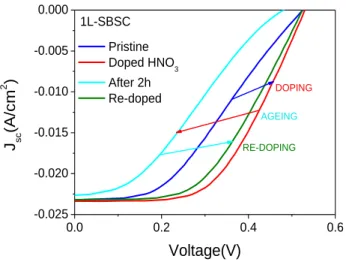
The J-V characteristics under illumination were acquired on the 1L-SBSC that showed the better performances in term of EQE in our experiments. The curves were acquired just after the fabrication (pristine cells) and after each doping process step (HNO3 doping, ageing and recovery), as already reported for Gr/n-Si SBSC [17]. The curves in Figure 7 show the effect of the different treatments on the behavior of 1L-SBSC. The relative electrical parameters are reported in Table 2. In Figure 7, the illuminated J-V characteristics clearly evidence the effect of doping on cell performance. The undoped cell shows a Voc ~ 0.52 V with a Rs of 17.5 Ω. The molecular doping improves the cell performance in particular in term of PCE and fill factor (FF), while reducing the Rs. The FF increases from 39.4 % to 54.2 %. The result is an increase of PCE from 4.8 % of the pristine cell to 6.7 % of the doped device. The Rs decreases from 17.5 to 7.8 Ω. The influence of doping on the short-circuit current density (Jsc) is negligible, as already observed in literature [11, 45]. 400 600 800 1000 0 10 20 30 40 50 60 650 700 750 800 59 60 61 SBSC OB 1L-SBSC OB 2L-SBSC OB SBSC 1L-SBSC 2L-SBSC EQ E(% ) Wavelength (nm)
Figure 7. Doping, ageing and recovery effect on illuminated J-V curve of 1L-SBSC: before the doping (blue), immediately after doping (red), after 2 hours (light blue) and
after re-doping process (green)
The improvements in the cell photovoltaic parameters by HNO3 treatment can be attributed to different factors. The molecular doping is expected to decrease the sheet resistance of graphene [11, 14] and this leads to a proportional decrease in the Rs of the solar cell, and to a concomitant increase in the FF. Beside the significant decrease in the graphene sheet resistance, a volatile oxidant treatment such as the exposure to HNO3 vapor is expected to improve the uniformity of the Schottky junction by saturating defects at the interfaces. This should also contribute to decrease the cell Rs, further increasing its FF [11]. The light blue curve in Figure 7 show the ageing effect on the cell. After 2 hours, the photovoltaic parameters show a worsening. Ageing degrades the Voc (reaching 0.48 V) and FF parameters and PCE decrease respectively at 32.7 and 3.5 %, increasing the S shape of the curve with the Rs that measures 32.3 Ω. This effect is due to the instability of the doping obtained by volatile acid compounds which causes lower SBH and hence decreases the value of Voc [11] as also reported for simple junction Gr/n-Si [17]. A quasi-complete recovery of photovoltaic parameters is possible upon repeating the exposure to HNO3 (green curve in Figure 7).
4. CONCLUSION
SBSC based on few-layer Gr/n-Si junction with single and double GBD interlayers were fabricated and characterized. J-V curves and EQE confirm that a single GBD layer improves the Schottky junction, by reducing the inhomogeneity at interface which acts as charge traps and add interface states and recombination centers. In 1L-SBSC, the saturation current and Rs are lowered, while the SBH increases from 0.78 to 0.87 V in comparison with SBSC. η was reduced from 2.15 to 1.6, as indicator of reduction of interface recombination centers. The EQE curves confirm the improvements derived by the insertion of single GBD interlayer in Gr/n-Si junction, in particular for measurements acquired in OB conditions. 1L-SBSC showed an EQE with a ∼20 % enhancement compared to SBSC. Doping treatment with HNO3 vapor (which p-dopes graphene) was performed on the 1L-SBSC, whose PCE reached 6.7 %. The degradation of the solar cells parameters measured after 2 hours of storage in air has been completely
recovered by re-exposing the cell to HNO3.
Table 2. Photovoltaic parameters calculated from curves reported in Figure 7 Process step Jsc (mA/cm2) Voc (V) FF (%) PCE (%) Rs (Ω) Pristine 23.1 0.52 39.4 4.8 17.5 Doped HNO3 3min 23.3 0.53 54.2 6.7 7.8 After 2h 22.6 0.48 32.7 3.5 32.3 Re-doped HNO3 3min 23.2 0.52 50.7 6.2 9.0
In the present work we highlight that the insertion of GBD interlayers can improve the interface between n-Si and conductive graphene, thus increasing the PCE. This work sets the basis for the exploration of solar cells fabricated with various absorbers and stacks of GBD films with selected properties, such as layer number, workfunction, charge transport behavior, and doping level.
REFERENCES
[1] Lin Y, Li X, Xie D, Feng T, Chen Y, Song R, Tian H, Ren T, Zhong M, Wang K, Zhu H. (2013). Graphene/semiconductor heterojunction solar cells with modulated antireflection and graphene work function. Energy and Environmental Science 6(1): 108–115. https://doi.org/10.1039/C2EE23538B
[2] Tao L, Chen Z, Li X, Yan K, Xu JB. (2017). Hybrid graphene tunneling photoconductor with interface engineering towards fast photoresponse and high responsivity. npj 2D Materials and Applications 1(1): 19. https://doi.org/10.1038/s41699-017-0016-4
[3] Li X, Zhu M, Du M, Lv Z, Zhang L, Li Y, Yang Y, Yang T, Li X, Wang K, Zhu H, Fang Y. (2015). High detectivity graphene-silicon heterojunction photodetector. Small 12(5): 595-601. https://doi.org/10.1002/smll.201502336
[4] Li X, Zhu H, Wang K, Cao A, Wei J, Li C, Jia Y, Li Z, Li X, Wu D. (2010). Graphene-on-silicon schottky junction solar cells. Advanced Materials 22(25): 2743-2748. https://doi.org/10.1002/adma.200904383
[5] Ihm K, Lim JT, Lee KJ, Kwon JW, Kang TH, Chung S, Bae S, Kim JH, Hong BH, Yeom GY. (2010). Number of graphene layers as a modulator of the open-circuit voltage of graphene-based solar cell. Applied Physics Letters 97(3): 32113. https://doi.org/10.1063/1.3464319 [6] Ye Y, Dai L. (2012). Graphene-based Schottky junction
solar cells. Journal of Materials Chemistry 22(46): 24224–24229. https://doi.org/10.1039/C2JM33809B [7] An X, Liu F, Kar S. (2013). Optimizing performance
parameters of graphene–silicon and thin transparent graphite–silicon heterojunction solar cells. Carbon 57329–337.
https://doi.org/10.1016/j.carbon.2013.01.080
[8] Yu X, Yang L, Lv Q, Xu M, Chen H, Yang D. (2015). The enhanced efficiency of graphene-silicon solar cells by electric field doping. Nanoscale 7(16): 7072–7077. https://doi.org/10.1039/C4NR06677D
[9] Song Y, Li X, Mackin C, Zhang X, Fang W, Palacios T, Zhu H, Kong J. (2015). Role of interfacial oxide in high-efficiency graphene–silicon schottky barrier solar cells.
0.0 0.2 0.4 0.6 -0.025 -0.020 -0.015 -0.010 -0.005 0.000 RE-DOPING AGEING J sc (A/cm 2 )
Voltage(V)
Pristine Doped HNO3 After 2h Re-doped 1L-SBSC DOPINGNano Letters 15(3): 2104–2110. https://doi.org/10.1021/nl505011f
[10] Miao X, Tongay S, Petterson MK, Berke K, Rinzler AG, Appleton BR, Hebard AF. (2012). High efficiency graphene solar cells by chemical doping. Nano Letters 12(6): 2745–2750. https://doi.org/10.1021/nl204414u [11] Cui T, Lv R, Huang Z-H, Chen S, Zhang Z, Gan X, Jia
Y, Li X, Wang K, Wu D, Kang F. (2013). Enhanced efficiency of graphene/silicon heterojunction solar cells by molecular doping. Journal of Materials Chemistry A 1(18): 5736–5740. https://doi.org/10.1039/C3TA01634J [12] Zhang X, Xie C, Jie J, Zhang X, Wu Y, Zhang W. (2013). High-efficiency graphene/Si nanoarray Schottky junction solar cells via surface modification and graphene doping. Journal of Materials Chemistry A
1(22): 6593–6601.
https://doi.org/10.1039/C3TA10203C
[13] Xie C, Zhang X, Ruan K, Shao Z, Dhaliwal SS, Wang L, Zhang Q, Zhang X, Jie J. (2013). High-efficiency, air stable graphene/Si micro-hole array Schottky junction solar cells. Journal of Materials Chemistry A 1(48): 15348–15354. https://doi.org/10.1039/C3TA13750C [14] Li X, Xie D, Park H, Zhu M, Zeng TH, Wang K, Wei J,
Wu D, Kong J, Zhu H. (2013). Ion doping of graphene for high-efficiency heterojunction solar cells. Nanoscale 5(5): 1945–1948. https://doi.org/10.1039/C2NR33795A [15] Li X, Xie D, Park H, Zeng TH, Wang K, Wei J, Zhong
M, Wu D, Kong J, Zhu H. (2013). Anomalous behaviors of graphene transparent conductors in graphene-silicon heterojunction solar cells. Advanced Energy Materials
3(8): 1029–1034.
https://doi.org/10.1002/aenm.201300052
[16] Li YF, Yang W, Tu ZQ, Liu ZC, Yang F, Zhang LQ, Hatakeyama R. (2014). Schottky junction solar cells based on graphene with different numbers of layers. Applied Physics Letters 104(4): 43903. https://doi.org/10.1063/1.4863683
[17] Lancellotti L, Bobeico E, Capasso A, Lago E, Delli Veneri P, Leoni E, Buonocore F, Lisi N. (2016). Combined effect of double antireflection coating and reversible molecular doping on performance of few-layer graphene/n-silicon Schottky barrier solar cells. Solar Energy 127(Supplement C): 198–205. https://doi.org/https://doi.org/10.1016/j.solener.2016.01. 036
[18] Shi E, Li H, Yang L, Zhang L, Li Z, Li P, Shang Y, Wu S, Li X, Wei J, Wang K, Zhu H, Wu D, Fang Y, Cao A. (2013). Colloidal antireflection coating improves graphene–silicon solar cells. Nano Letters 13(4): 1776– 1781. https://doi.org/10.1021/nl400353f
[19] Feng T, Xie D, Lin Y, Zang Y, Ren T, Song R, Zhao H, Tian H, Li X, Zhu H, Liu L. (2011). Graphene based Schottky junction solar cells on patterned silicon-pillar-array substrate. Applied Physics Letters 99(23): 233505. https://doi.org/10.1063/1.3665404
[20] Yang L, Yu X, Xu M, Chen H, Yang D. (2014). Interface engineering for efficient and stable chemical-doping-free graphene-on-silicon solar cells by introducing a graphene oxide interlayer. Journal of Materials Chemistry A 2(40): 16877–16883. https://doi.org/10.1039/C4TA02216E [21] Tsuboi Y, Wang F, Kozawa D, Funahashi K, Mouri S,
Miyauchi Y, Takenobu T, Matsuda K. (2015). Enhanced photovoltaic performances of graphene/Si solar cells by insertion of a MoS2 thin film. Nanoscale 7(34): 14476–
14482. https://doi.org/10.1039/C5NR03046C
[22] Xu D, He J, Yu X, Gao D, Ma L, Mu X, Zhong M, Xu Y, Ye J, Xu M, Yang D. (2017). Illumination-induced hole doping for performance improvement of graphene/n‐silicon solar cells with P3HT interlayer. Advanced Electronic Materials 3(3): 1600516. https://doi.org/10.1002/aelm.201600516
[23] Bhopal MF, Akbar K, Rehman MA, Lee D won, Rehman A ur, Seo Y, Chun SH, Lee SH. (2017). High-ĸ dielectric oxide as an interfacial layer with enhanced photo-generation for Gr/Si solar cells. Carbon 12556–62. https://doi.org/https://doi.org/10.1016/j.carbon.2017.09. 038
[24] Alnuaimi A, Almansouri I, Saadat I, Nayfeh A. (2018). High performance graphene-silicon Schottky junction solar cells with HfO2 interfacial layer grown by atomic layer deposition. Solar Energy 164174–179. https://doi.org/10.1016/j.solener.2018.02.020
[25] Lancellotti L, Sansone L, Bobeico E, Lago E, Noce MD, Veneri PD, Borriello A, Casalino M, Coppola G, Giordano M, Iodice M. (2015). Graphene oxide as an interfacial layer in silicon based Schottky barrier solar cells. In: 2015 Fotonica AEIT Italian Conference on Photonics Technologies, pp 1–4.
[26] Xie C, Zhang X, Wu Y, Zhang X, Zhang X, Wang Y, Zhang W, Gao P, Han Y, Jie J. (2013). Surface passivation and band engineering: a way toward high efficiency graphene-planar Si solar cells. Journal of Materials Chemistry A 1(30): 8567–8574. https://doi.org/10.1039/C3TA11384A
[27] Ma J, Bai H, Zhao W, Yuan Y, Zhang K. (2018). High efficiency graphene/MoS2/Si Schottky barrier solar cells using layer-controlled MoS2 films. Solar Energy 16076– 84. https://doi.org/10.1016/j.solener.2017.11.066 [28] Meng JH, Liu X, Zhang XW, Zhang Y, Wang HL, Yin
ZG, Zhang YZ, Liu H, You JB, Yan H. (2016). Interface engineering for highly efficient graphene-on-silicon Schottky junction solar cells by introducing a hexagonal boron nitride interlayer. Nano Energy 2844–50. https://doi.org/10.1016/j.nanoen.2016.08.028
[29] Capasso A, De Francesco M, Leoni E, Dikonimos T, Buonocore F, Lancellotti L, Bobeico E, Sarto MS, Tamburrano A, De Bellis G, Lisi N. (2014). Cyclododecane as support material for clean and facile transfer of large-area few-layer graphene. Applied
Physics Letters 105(11): 113101.
https://doi.org/10.1063/1.4895733
[30] Capasso A, Dikonimos T, Sarto F, Tamburrano A, De Bellis G, Sarto MS, Faggio G, Malara A, Messina G, Lisi N. (2015). Nitrogen-doped graphene films from chemical vapor deposition of pyridine: influence of process parameters on the electrical and optical properties. Beilstein Journal of Nanotechnology 62028–2038. https://doi.org/10.3762/bjnano.6.206
[31] Capasso A, Salamandra L, Faggio G, Dikonimos T, Buonocore F, Morandi V, Ortolani L, Lisi N. (2016). Chemical vapor deposited graphene-based derivative as high-performance hole transport material for organic photovoltaics. ACS Applied Materials & Interfaces
8(36): 23844–23853.
https://doi.org/10.1021/acsami.6b06749
[32] Faggio G, Capasso A, Messina G, Santangelo S, Dikonimos T, Gagliardi S, Giorgi R, Morandi V, Ortolani L, Lisi N. (2013). High-temperature growth of
graphene films on copper foils by ethanol chemical vapor deposition. The Journal of Physical Chemistry C
117(41): 21569–21576.
https://doi.org/10.1021/jp407013y
[33] Lisi N, Dikonimos T, Buonocore F, Pittori M, Mazzaro R, Rizzoli R, Marras S, Capasso A. (2017). Contamination-free graphene by chemical vapor deposition in quartz furnaces. Scientific Reports 7(1): 9927. https://doi.org/10.1038/s41598-017-09811-z [34] Lancellotti L, Bobeico E, Capasso A, Noce M Della,
Dikonimos T, Lisi N, Veneri PD. (2014). Effects of HNO3 molecular doping in graphene/Si Schottky barrier solar cells. In: 2014 Fotonica AEIT Italian Conference on Photonics Technologies. 1–3.
[35] Ferrari AC, Meyer JC, Scardaci V, Casiraghi C, Lazzeri M, Mauri F, Piscanec S, Jiang D, Novoselov KS, Roth S, Geim AK. (2006). Raman spectrum of graphene and graphene layers. Physical Review Letters 97(18): 187401. https://doi.org/10.1103/PhysRevLett.97.187401 [36] Santangelo S, Messina G, Malara A, Lisi N, Dikonimos T, Capasso A, Ortolani L, Morandi V, Faggio G. (2014). Taguchi optimized synthesis of graphene films by copper catalyzed ethanol decomposition. Diamond and Related
Materials 4173–78.
https://doi.org/10.1016/j.diamond.2013.11.006
[37] Ferrari AC. (2007). Raman spectroscopy of graphene and graphite: Disorder, electron–phonon coupling, doping and nonadiabatic effects. Solid State Communications 143(1): 47–57. https://doi.org/10.1016/j.ssc.2007.03.052 [38] Pimenta MA, Dresselhaus G, Dresselhaus MS, Cancado LG, Jorio A, Saito R. (2007). Studying disorder in graphite-based systems by Raman spectroscopy.
Physical Chemistry Chemical Physics 9(11): 1276–1290. https://doi.org/10.1039/B613962K
[39] Seifert M, Vargas JEB, Bobinger M, Sachsenhauser M, Cummings AW, Roche S, Garrido JA. (2015). Role of grain boundaries in tailoring electronic properties of polycrystalline graphene by chemical functionalization. 2D Materials 2(2): 24008. https://doi.org/10.1088/2053-1583/2/2/024008
[40] Wang Y, Xu X, Lu J, Lin M, Bao Q, Özyilmaz B, Loh KP. (2010). Toward high throughput interconvertible graphane-to-graphene growth and patterning. ACS Nano 4(10): 6146–6152. https://doi.org/10.1021/nn1017389 [41] Tung RT. (2001). Recent advances in Schottky barrier
concepts. Materials Science and Engineering: R: Reports 35(1): 1–138. https://doi.org/10.1016/S0927-796X(01)00037-7
[42] Tung RT. (2014). The physics and chemistry of the Schottky barrier height. Applied Physics Reviews 1(1): 11304. https://doi.org/10.1063/1.4858400
[43] Werner JH, Güttler HH. (1991). Barrier inhomogeneities at Schottky contacts. Journal of Applied Physics 69(3): 1522–1533. https://doi.org/10.1063/1.347243
[44] Di Bartolomeo A, Luongo G, Giubileo F, Funicello N, Niu G, Schroeder T, Lisker M, Lupina G. (2017). Hybrid graphene/silicon Schottky photodiode with intrinsic gating effect. 2D Materials 4(2): 25075. https://doi.org/10.1088/2053-1583/aa6aa0
[45] Lancellotti L, Bobeico E, Castaldo A, Delli Veneri P, Lago E, Lisi N. (2018). Effects of different graphene dopants on double antireflection coatings/graphene/n-silicon heterojunction solar cells. Thin Solid Films 64621–27. https://doi.org/10.1016/j.tsf.2017.11.018