Università degli Studi di Roma “Tor Vergata”
Dipartimento di Ingegneria Meccanica
Dottorato di Ricerca in Ingegneria dei Microsistemi
XVII Cycle
C
C
H
H
A
A
R
R
A
A
C
C
T
T
E
E
R
R
I
I
Z
Z
A
A
T
T
I
I
O
O
N
N
O
O
F
F
P
P
I
I
E
E
Z
Z
O
O
R
R
E
E
S
S
I
I
S
S
T
T
I
I
V
V
E
E
P
P
R
R
O
O
P
P
E
E
R
R
T
T
I
I
E
E
S
S
I
I
N
N
C
C
V
V
D
D
D
D
I
I
A
A
M
M
O
O
N
N
D
D
F
F
I
I
L
L
M
M
S
S
T
T
O
O
B
B
E
E
U
U
S
S
E
E
D
D
A
A
S
S
S
S
T
T
R
R
A
A
I
I
N
N
G
G
A
A
U
U
G
G
E
E
Candidate
Ing. Gonzalo Rodríguez
Coordinator
Tutor
Acknowledgements
In first place I want to acknowledge and to be thankful to my Family and Maria Laura, my Fiancée and future Wife, for all the support, patience, push and love with which have accompanied me in this demanding period of my life. Without your support I couldn't never have succeed; for all of you my love, admiration and eternal gratitude.
I also want to gratefully acknowledge Prof. Antonio Paoletti, Prof. Aldo Tucciarone, Prof. Enrico Milani, Prof. Marco Marinelli, Dr. Gianluca Verona Rinati and my doctorate companions Gianluca Pucella and Antonio Balducci for introducing me in microsystems field, in particular regarding the physics of diamond and their possible applications, and for their patient tutoring and support in developing my research activities. Moreover, I want to gratefully acknowledge my companions for their critical analysis in writing the present work. At this point I want to underline the tutoring in experimental activities in the laboratory and their theoretical continuously support essential in the development of this thesis work. I also want to emphasize and to thanks for helping me in the growth that I have had like person and professional in these three years.
At the end a special thanks for all the person that have been near me inside or outside the university in this PhD period in a foreign country; this work is also for you.
“Si pude ver más lejos es porque estoy parado sobre hombros de gigantes”
“If I could see further is because I’m standing over giants’ shoulders”
Isaac Newton
A mis Padres: “Ustedes son mis Gigantes”
To my parents: “You are my Giants”
Contents
Introduction...7
Chapter 1
The Microsystems
Summary... ...111.1. THE MICROSYSTEMS ...….12
1.2. APPLICATION AND ADVANTAGES OF MICROSYSTEMS…...13
1.3. MICROSYSTEM MANUFACTURE…...16 1.4. DEPOSITION TECHNIQUES...…17 1.5. LITHOGRAPHIC METHOD...…..19 1.6. REMOVAL METHODS...20 1.6.1. Etching...…...21 1.6.2. Laser micromachining...…..22
1.7. ADVANCED ELABORATION METHODS...23
Chapter 2
The Diamond
Summary...252.1 DIAMOND AS ALTERNATIVE MATERIAL TO SILICON……...….26
2.2 DIAMOND PROPERTIES...……...27
2.2.1 Resistance to harsh environments...……...28
2.2.2 Mechanical properties...……...29
2.2.3 Electronic properties...……….29
2.2.4 Thermal properties...……..30
2.2.5 Optical properties...……...31
2.3 DIAMOND GROWTH...………...31
2.4 HIGH PRESSURE AND HIGH TEMPERATURE (HPHT) GROWTH METHOD...32
2.5 LOW PRESSURE GROWTH METHODS...……...…33
2.5.1 Hot filament method...………….33
2.5.2 Combustion flame deposition...…....34
2.5.3 Plasma jet deposition...…....35
2.5.4 Plasma enhanced deposition...……...36
2.6 CVD DIAMOND FILMS PRODUCTION...………...38
2.6.1 CVD diamond growth and nucleation...……….38
2.6.2 C/H/O diagram...……….40
2.6.3 Optimisation of growth parameters...……….41
Chapter 3
Growth and characterization of boron – doped CVD
diamond films
Summary...….45
3.1 USED EQUIPMENT IN CVD DIAMOND P-TYPE DOPING...46
3.2 CONDUCTION MECHANISMS IN P-DOPED CVD DIAMOND FILMS...….48
3.3 CHARACTERIZATION OF P-DOPED DIAMOND FILMS...50
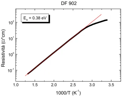
3.3.1 Characterization through R(T) measurements...….52
3.3.2 Temperature coefficient of resistance (TCR)………...54
3.4 DOPING GROWTH CHAMBER DYNAMICS...………...55
3.4.1 Doped at once and growing systematic study...………..56
3.4.2 Doped at once and growing in presence of methanol systematic study...…..58
Chapter 4
Piezoresistive effect in boron – doped CVD diamond
films
Summary...624.1 MICROSENSORS…...…….63
4.1.1 Sensor response curve ...……….64
4.1.2 Internal sensitivity (iS)...……….65
4.1.3 Resolution, noise and drift ...………....66
4.2 BAND THEORY OF PIEZORESISTIVE EFFECT...……….68
4.2.1 Numeric approach of piezoresistive effect...……….69
4.3 OPPORTUNITIES FOR DIAMOND AS A PIEZORESISTIVE SENSOR...73
4.3.1 Diamond-based strain gauges...………....73
4.3.2 Diamond-based pressure sensors...………...75
4.3.3 Diamond-based accelerator...………....77
Chapter 5
Experimental setup of piezoresistive effect
demonstrator
Summary...795.1 DEMONSTRATOR APPARATUS DESCRIPTION...…...80
5.1.1 Force application system...………...81
5.1.2 Thermal regulation...………...82
Chapter 6
Time response of boron – doped CVD diamond films
Summary...85
6.1 I-V CHARACTERISTIC...………..86
6.2 APPARENT HYSTERESIS EFFECT ON DATA ACQUISITION PAUSE...….87
6.3 EFFECT OF TEMPERATURE IN TIME RESPONSE ...………....88
6.4 EFFECT OF THE APPLIED STRAIN IN TIME RESPONSE...………89
6.5 TIME RESPONSE AS A FUNCTION OF TEMPERATURE AND DOPING LEVEL OF BORON DOPED CVD DIAMOND FILMS...………90
6.6 EXPERIMENTAL ACQUISITION PAUSE TIME SELECTION...………...92
Chapter 7
Experimental results of piezoresistive measurements
Summary...…947.1 INTRODUCTION...……….95
7.2 TEMPERATURE DEPENDENCE OF I-V CHARACTERISTIC...….96
7.3 RELATIVE CHANGE OF RESISTANCE AS A FUNCTION OF APPLIED STRAIN.………….97
7.4 RELATIVE CHANGE OF RESISTANCE AS A FUNCTION OF DOPING LEVEL...…..98
7.5 STUDY OF PIEZORESISTIVE PROPERTIES OF PECVD P-DOPED DIAMOND AT HIGH TEMPERATURES..………...…99
Conclusions...106
INTRODUCTION
The increasing exigency of more automated and easier to use devices suppose the fabrication of systems able to measure some physical or chemical quantities and to react in consequence automatically, operating, then, in a partially autonomous way. For this particular interest, in the last years, big efforts were made in order to develop Microsystems. With “Microsystems” we intend a miniaturized system made of one or more sensors that put in evidence and measure physical and chemical magnitudes, producing a signal that is opportunely processed and used for accomplishing a well established electrical, optical, chemical or mechanical function.
Microsystems could be considered as a result of the integration methodologies and technologies belonging to mechanics, electronics and informatics, joined in design and construction steps allowing the realization of cheapest, simplest, more reliable and more flexible devices. The possibility of integrating mechanical and electronic components in the same device has established a radical change in the project philosophy of a large number of products. For this reason, microsystem technologies represent the methodological and technical support that better characterize high number of sectors technologically advanced (i.e.: Autronics, industrial automation, consumer electronics, mobile communications and health).
Current microsystem technology is related almost exclusively to silicon. This material presents very important electronic characteristics besides its good mechanical properties. Moreover, the use of silicon in microelectronics has established an important knowledge of this material and related technologies. Then, the base technologies for the realization of microsystems are those developed for the manufacturing of integrated circuits based on silicon., it means, lithography, chemical attacks and film growing. These
technologies afterwards allowed the development of specific microsystems technologies, derived from precision mechanics and other sectors as physics.
However, there are limits to mechanical, thermal and electrical properties of silicon for specific applications in which the capability to operate at high temperature and to resist high radiation flux or chemical attacks is important. In order to compare the new technological challenges in the realization of devices for novel applications, research and development of new materials are needed. Diamond and in particular polycrystalline
diamond, produced with CVD (Chemical Vapor Deposition) technique, is without any
doubt an outstanding material in its mechanical, optical, thermal and electronic properties, that makes it very interest for different applications. Moreover, due to the high bandgap between valence band and conduction band (apt to operate at high temperatures or in presence of light) and because of its outstanding physical and electronic properties, as it high fusion point, its low chemical reactivity and it extreme robustness, diamond seems to be a natural candidate to be used in harsh/hostile environment. Obviously, in order to take advantage of all its possible applications it is important to have good quality diamond, thus it is mandatory the study of diamond physical properties, with the goal of better understand its characteristics at high temperature that constitutes a harsh environment.
In this context is placed the present PhD thesis. It is centered on the study of diamond doping and piezoresistive effect on boron doped p-type diamond grown at the Mechanical Engineering Department of the University of Rome “Tor Vergata” laboratories. This work also presents a study of the mentioned effect at high temperature in order to establish some parameters that must be taken into account for the realization of potential strain gauge apt to be used at high temperature.
In particular, this work is developed in seven chapters. In the first one there is an introduction to microsystems, with references to the advantages that offer and the different
possible applications. Later the main fabrication techniques are presented, beginning from those derived from microelectronics to that specific of microsystems. In the second chapter diamond properties are analyzed, focusing on that properties that make diamond an outstanding material for the realization of microsystems apt to be used in harsh/hostile environments. Also in the second chapter, main synthesis processes of artificial diamond are analyzed, among them plasma enhanced CVD technique, that is the one used at the Mechanical Engineering Department of the University of Rome “Tor Vergata” laboratories for the growth of diamond film.
In the third chapter it is described the growth and Boron doping process that lead to obtain p-type doped diamond samples, it is described in detail the necessary equipment, the growth conditions and the parameters that must be taken into account in order to manage a doping growth. It is also described the theory behind the experimental facts, especially described that of conduction mechanisms in doped diamond; characterization through R(T) and experimental results are shown. Always in third chapter Temperature
Coefficient of Resistance (TCR) will be defined and calculated and evaluated its behavior
with different doping levels, we will also see its importance in future measurements due to its capability of hiding piezoresistive effect. Moreover, systematic studies of the chamber dynamics is also presented, both with methanol in the growth chamber and without it, it is notice that methanol content act as an inhibitor in doping efficiency, because of its oxygen content that combine the residual boron (in the chamber) to produce boron oxide (B2O3).
The fourth chapter describes the theory of piezoresistive effect that is the main effect analyzed in this work. First of all, it is described the main response parameters affecting the operation of any sensor device that are sensor response curve, internal sensitivity and resolution, noise and drift. Moreover a numerical approach to piezoresistive effect is presented, that gives the reader a self-content description of the main parameters
involved in piezoresistive effect; after that, some motivations are presented to give the reader the whole picture in which Boron-doped diamond based strain gauge could be used.
The last three chapters are dedicated to the main application of this PhD work that is the development of a demonstrator able to show the mentioned effect and the potentiality for making diamond based strain gauges. In particular the fifth chapter is intended to describe the experimental setup of the demonstrator apparatus, in which it is explained its construction, its functionality, the force application system and its thermal regulation, moreover, diagrams and pictures are also presented in order to enlighten how it works and what we can expect from measurements. Later in the sixth chapter, time response of diamond samples is analyzed; this chapter has two main scopes, the first is investigate the time response as a function of different parameters that could be real work conditions of a potential strain gauge (i.e.: temperature, strain, doping level). The other scope is to established the pause needed for the sample to reach the steady state when voltage is varying, that is, in order to make I-V measurements voltage must be varied (through a programmable voltage source) then a pause must be done in order to allow diamond to stabilized and then make data acquisition. In the last chapter, the main results of piezoresistive effect on diamond samples grown at the Mechanical Engineering Department of the University of Rome “Tor Vergata” laboratories are presented, I-V characteristic were performed in order to study the electrical behavior of diamond samples; relative change of resistance (∆R R) and gauge factor (GF) are presented as a function of doping level and applied strain; moreover, in order to analyze diamond behavior at high temperature, measurements were made, in which, we will see the capability of diamond as sensing material apt to be used in harsh environments. Studies of the variation of ∆R R
Chapter 1
The Microsystems
Summary
The development of microelectronics technologies and their integration with mechanical, optical, chemical or biological systems have made grow, specially in the last decade, the interest in microsystems, it means miniaturized systems composed by sensors which measure a physical or chemical magnitude then converting this measure in an electrical signal. This signal is properly elaborated through integrated electronics in the same sensor and sent to an actuator who performs the desired command.
The use of microsystems offer interesting advantages: more functionality and reliability, less power consumption, little dimensions and weight, low cost and flexibility in design and production stages. However, mass production, at the moment, is only available for a few numbers of sectors of interest, i.e. autronics, industrial automation, consumer electronics, mobile communications and biomedicine.
The most useful material for microsystems production is the silicon, because of their good mechanical and electronic properties, that allowed all the production technologies from the microelectronics to be used, with other specific technologies developed ad-hoc from precision mechanics and physics, in microsystems production.
1.1 THE MICROSYSTEMS
The possibility of integrating microelectronics technologies with mechanical, optical, chemical or biological systems in miniaturized structures, supporting by the exigency of obtaining high functional complexity and very low dimensions devices, has made develop, in the last years, a particular interest to the microsystems.
The term microsystem indicates a miniaturized system composed of sensors which measure chemical and physical magnitudes then converting such magnitudes in an
electrical signal, an integrated circuit with analyzer functions of signal processing and one or more actuators with the received command from the analyzer execute different actions to the external environment [1,2]. The general scheme of a microsystem is illustrated in Fig 1.1. EXTERNAL ENVIRONMENT MICROMECHANISM MICROACTUATOR INTERFACE MAN-MACHINE PROCESSING CONTROLLING MICROSENSORS USER EXTERNAL ENVIRONMENT MICROMECHANISM MICROACTUATOR INTERFACE MAN-MACHINE PROCESSING CONTROLLING MICROSENSORS USER
Fig. 1.1 General scheme of a microsystem.
Microsystems can be considered derivatives from the complementary use, at miniaturized level, of electronic, mechanical, optical, biological and informatics technologies, for which one of the fundamental characteristic is the multidisciplinary knowledge that is needed in order to develop a device.
It’s clear that the degree of “intelligence” of a microsystem is higher as higher is the capability of interacting, autonomously with the surrounding environment, in an fast and efficiency way due to the integration of a number always higher of sensors, processors and actuators. That explains the miniaturization trend always find in microsystems, an analogous thing happens in microelectronics, with the noted complication of the microsystem integration with electric, optical, mechanical and chemical functions.
1.2 APPLICATIONS AND ADVANTAGES OF MICROSYSTEMS
The use of microsystems offers a very interesting series of advantages from a point of view of application: higher functionality, due to the electric and non-electric functions integration in very low spaces; higher reliability, due to the high integration between components; low power consumption, low weight and dimensions, low cost and high flexibility in project and production stages.
The microsystems are recently incorporated in the industrial production frame in order to satisfy different needs in a wide spectra application [3-5]. So, mass production is at the moment for a few industrial production sectors, such as, autronics, industrial automation, consumer electronics, mobile communications and biomedicine.
The autronics represent without a doubt the highest production volume and in
which microsystems find the highest number of applications (historically is the field in which were first applied as exhaust gas microsensors in catalyzed systems in vehicles). It was anticipated that in a few years sensors and electronic components will represent approximately the 30% of the value of a car, moreover, the present applications are in a very wide range: accelerometers, pressure sensors, temperature, air and carburant flows, exhaust gas, are nowadays integral part of a modern car.
Combustion chamber and tires control systems are needed to be solved with microsystems, are also needed in exhaust catalyzed systems, ABS (Anti-lock Braking System), Anti-slide system, active damping system, airbag protection system for passengers, all of these systems widely use pressure sensors for its operation.
In the field of industrial automation microsystems are fundamental in robotics and in fields incompatible with human intervention. In this market area will be highly required in near future products such as: pressure sensors, accelerometers, flow sensors, structural damage monitors and chemical sensors apt to measure specific concentration of chemical species.
Consumer electronics and mobile communications with miniaturized transmission
systems, recording and reproduction data systems, high definition visualization and printing systems are able fields to absorb high production volumes.
Another development microsystems area is represented by biomedicine, where microsystems could completely revolutionize this application field.
At the moment microsystems are highly necessary for artificial organs control, microsurgery, auditory support advice, stimulation of implanted nerves and recently for liquid analysis and drug automatic and intelligent provision control systems (i.e.: insulin for diabetics). It’s clear that a point of fundamental importance is the biocompatibility for which is a main role the R&D in new materials.
An area which is believed to have a strong expansion, with a strong industrial stimulus because of commercial possibilities is the domotics. In this field microsystems will allow more comfortable, cheaper and highly safer all the activities in domestic environment thanks to automation systems (i.e.: selective sensors of temperature, humidity, pH control), gas flow and liquids control devices, security sensors for identification of gas presence (i.e.: carbon monoxide or methane).
Microsystems will be able to contribute essentially in environment control: they will contribute in different ways to environmental protection, through miniaturized systems for water and air monitoring (chemical sensors), the study of chemical and physical properties of used substances, analysis and control of emissions (for vehicles and rooms) and monitoring of contamination by environmental radiation.
Agriculture, at the end, will be in conditions of taking advantages from devices which will be able to do land control from nutritious and polluting agents, maturation degree and possible presences of diseases in vegetal products (from appearance of individual diseases or epidemical ones), moreover, production related controls and quality in industrial treatment of foods.
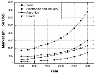
We close this paragraph reporting in Fig 1.2 an idea of the dimension of the microsystem market in the United States related to the three greater sectors in volume production [6]. 1994 1996 1998 2000 2002 2004 0 500 1000 1500 2000 2500 3000 3500 4000 M ar ke t (m illi o n U $S ) Year Total
Electronics and industry Autronics
Health
1.3 MICROSYSTEM MANUFACTURE
The material mainly used in microsystem manufacture is silicon, which besides being an optimal semiconductor presents satisfactory mechanical properties [7]. In addition, the good knowledge of this material, acquired in microelectronics development, allows the use in microsystem production of all manufactures technologies typical from microelectronics, for example lithography, chemical attack and film growing. The use of silicon guarantees the best possible integration between mechanical and electric components, for which, it’s possible to produce in a silicon substrate micromechanical devices and integrate, on the same substrate, control electronics.
However, it’s important to underline that for microsystems production, besides using all typical technologies from microelectronics, is necessary to use some other technologies specific of microsystem derived from precision mechanics (microstereolitography) or some from another area such as physics (laser micromachining, LIGA technique). In fact, traditional techniques for manufacture and working of silicon microstructures are not always sufficient for the manufacture of microelectromechanical devices, because they are essentially planar type techniques which doesn’t allow the manufacture of really three-dimensional structures for mechanical and electronic functions.
In Fig. 1.3 is shown a general scheme of microsystem manufacture, which has mainly three phases: a phase of deposition, one of lithography and another one of material removal.
DEPOSITION REMOVAL SUBSTRATE FILM PHOTORESIST LITHOGRAPHY DEPOSITION REMOVAL SUBSTRATE FILM PHOTORESIST LITHOGRAPHY
Fig. 1.3 Base process in microsystem elaboration: Material layer are
deposited, the pattern is transferred onto the photoresist then removal of surface and bulk material. The process is repeated till complete the desired microstructure.
In particular, the three phases are repeated until completing the microstructure. Let us analyze separately the three phases of a microsystem manufacture.
1.4 DEPOSITION TECHNIQUES
The traditional technology for electronic microdevices manufacturing is based on the deposition and microelaboration of silicon substrates, dielectrics (ex: SiO2) and metals
(typically Al, but Ag and Au too). So, for the deposition of any device is essential to have the possibility of depositing substrates of this materials. Let us consider some of the more diffuse techniques for the elaboration of metallic layers and dielectric layers, noticing that the use of a particular technique instead another strongly depends on the kind of layer that has to be done [8].
The most common process for contact deposition and different metallic layers deposition is the thermal evaporation, which is based on the vacuum evaporation of the material to deposit.
The substrate on which it is wanted to deposit the material is placed near the evaporation source, which is heated with a thermal heater or through an electron beam. This technique allows obtaining high quality and a high directionality of the deposited layer.
The Chemical Vapor Deposition (CVD) is the most used technique for depositing silicon oxide, because it produces high isotropic layers avoiding problems of “shades” still in presence of cavities and complex morphologies and because allows, quickly, depositing large areas. The CVD is essentially based on the “reaction” of some gases in a high temperature chamber (400 / 600 °C); in individual, one of the reaction products is the compound that is wanted to be produced which is deposited on a wafer who acts as the substrate. The system is mainly constituted of a furnace that is filled and regulated with the necessary gases. For example, silicon oxide is deposited through the following reaction:
SiH4 + O2 → SiO2 + 2H2
Polycrystalline silicon can also be produced taking advantage of the CVD technique; in this case the system operates in a range of temperature between 600 – 650 °C and it is verified a reaction of molecular division of the SiH4 induced by thermal agitation:
SiH4 → Si + 2H2.
The sputtering indicates the technique based on the production of ions of the
material to deposit by effect of inert ion collisions opportunely accelerated (generally Argon ions) against the surface of the material to deposit [9,10]. A general scheme for a sputtering apparatus is essentially composed of two electrodes between which it is applied a potential difference; the material to deposit is normally positioned on the cathode, the Ar ions, produce at low pressure and temperature through electrical discharges or radio frequency, are accelerated by the potential difference and hit the material to deposit causing the cession of atoms which fill the substrate to cover.
1.5 LITHOGRAPHIC METHOD
Once deposited a layer on the substrate the next step is the microsystem realization, that consists of covering the layer with a photosensitive substance (resist) and “design” on the resist the structure (pattern) of the object to be produced on the substrate. The main technique used to transfer the pattern in the resist is the lithography; this technique consists of making a mask on which the structure is transferred to make in the resist. In this point the mask is illuminated through an opportune radioactive source and thus resist comes made an impression from the image of the pattern. In the other hand, the pattern must be transferred on the substrate, for which, at we will see, the lithographic process is followed of a process of removal of the parts no masked, that removal could be accomplished by chemical attack techniques, plasma techniques or optical techniques (laser) [11]. In the removal process the non-impressed resist is used as a protective mask against the removal of the material below.
The lithographic process could be done in different ways depending on the type of radiation used.
In the optical lithography ultraviolet radiation (200 – 400 nm) is used, the transfer of the pattern to the mask could be done putting the mask in contact (or almost in contact) with the photoresist (contact and proximity printing), or through projection techniques. In the case of contact printing resolutions of the order of the micron could be reached but it’s possible to have a mask damage due to the physical contact with the photoresist; it’s why proximity printing is safer, because physical contact between mask and photoresist is avoided, in the other hand, resolution is lower (2 – 5 µm).
At the end, in the projection method the mask damage is limited because the substrate is placed at several centimetersfrom the mask, and the worsening of the resolution due to the diffusion of the radiation could be compensated using a bigger dimension mask, because in
projection phase the dimension of the object projected could be reduced, that allows to obtain resolutions similar to the contact lithography.
The X-ray lithography [12,13] is similar to the optic one, in particular, to use X-ray
(RX) allows obtaining very high resolutions (till 0.1 µm) and producing deeper structures. The main difficulty in using RX is the physical duration of the mask, being impossible to use projection techniques.
In the electron beam lithography [11] the resist is printed by an electron beam
electronically controlled for which is not necessary the mask for pattern transfer. This technique offers, in principle, a greater resolution with respect to optical lithography, because the wavelength of an electron beam of energies of 20 – 50 keV is inferior to1 nm. In fact, resolution limit, in this type of lithography, is established by other factors, for ex: electron scattering inside the material below the resist (because of this electrons can print zones next to the one of interest), the aberration of the electrical and magnetic lenses used to focus the beam on the interest area, the magnetic interaction between electrons of the beam, resist properties, etc. This effect limits the resolution to 200 – 300 nm approximately, in order to diminish the resolution below 200 nm it is necessary to use an ion beam (that as is known they present lower ranges and more linear trajectories in the matter that the electrons), but of more complex use.
1.6 REMOVAL METHODS
Once finished the process of lithographic reproduction of the structure of the object to make, starts the true and the own one “mechanical” elaboration, in order to transfer the pattern from the resist to the substrate; the more used methods in this step are the etching and the laser micromachining.
1.6.1 Etching
Almost all lithographic processes use for micro-elaboration the as known etching, which is in practice the removal of the unprotected parts from the resist, with the objective to obtain the desired structure on the substrate. In particular, there are different types of etching.
The chemical etching [14] or wet etching, it’s a “chemical” attack method from
reagents in liquid solution that previews two steps: in the first step it is performed an oxidation process of the surface through oxidizing agents such as nitric acid (HNO3), this
step is followed by the step of dissolution of oxide through a proper dissolvent (HF, CH3COOH). In particular, on the base of the technique of bulk micromachining are the
principles of the anisotropic chemical attack, which is based in the properties of some chemical agents of different attack speed related to the crystallographic orientation from the material to be attacked (for ex: there is a 100 factor in the attack speed of the KOH for (100) and (111) planes of the silicon): taking advantage of this property it is possible to produce well defined structures. It is opportune to remember that most of the materials present a polycrystalline structure, so, for this materials the chemical attack is mainly isotropic and inevitably will be attacked under the resist profile giving rise to undercutting effects, it means the non-desired part removal of the material; therefore this etching type is not adapted to high spatial resolution elaboration (in general the obtained resolution is in the order of the thickness of the layer to be attacked) and for very deep attacks.
An etching that is distinguished for his enunciated anisotropy is the plasma assisted
etching [14,15] or dry etching, which is a “mechanical” etching that consists mainly in the
ion-surface interaction which allows to remove the non-desired material. In particular, one of the used techniques is that of the “back sputtering” and is in practice the reverse one of the sputtering. In this case the substrate with the material to be removed is placed on the
cathode, where the accelerated argon ions produce the sputtering reaction removing the non-desired material. As it was told, the advantage of this kind of etching is essentially the possibility of making highly anisotropic etching, due to the fact that all reactions are made in preferential way in the orthogonal direction of the substrate.
1.6.2 Laser micromachining
Between the microelaboration techniques, one of most diffuse is the laser
micromachining, which belongs to the family of the elaboration by material removal. In
particular, this technique, which can be used for different materials, consists in the material removal through the focalization of a laser beam. It is important to notice that it is a thermal process and the material is removed by fusion and evaporation, for which the excessive heating can damage the surrounding zones to the radiated one.
In order to solve this kind of problems and to improve the resolution of the elaboration, it is developed gradually the excimer laser microlithography [16], in which is used a laser that emits photons between 130 and 350 nm. This technique is in principle similar to the traditional optical technique, nevertheless presents some advantages mainly referred to the type of physical interaction between the laser beam and the photoresist. In fact, because of the high energy density of the laser beam, this is in degree of breaking the molecular unions from the molecules directly exposed to the radiation, creating a fast dissociation and a fast expulsion of the material by ablation, but without attacking adjacent molecules. This fact allows to obtain much more defined contours and to reduce the exposed surface to a strong heating, then avoiding the damage of the surrounding zones to the radiated one. In particular, the transfer of the pattern could be done using a mask, generally made of an amorphous quartz substrate (SiO2) covered with chromium layers
smaller wavelength they do not transmit the radiation), which directly, varying the speed of the sample with respect to the laser, the intensity of employed energy and the number of hits in every point, allows to obtain by this way very complex structures.
1.7 ADVANCED ELABORATION METHODS
Between the technologies of advanced type, arisen from the necessity to make three-dimensional structures for the manufacture of microsystems, the most used is without a doubt the LIGA [17] (Lithographie Galvanoformung Abformung). The LIGA is a manufacture technique based on a combination of X-ray lithography, with deep material attack, electric mold preparation and stamping. In particular, the structure is made exposing to the RX, through a mask, a photosensitive polymer layer (such as polymethyl meth-acrylate, PMMA) placed on a substrate. At this point, after removal the exposed parts through washing in an opportune chemical solution, it is possible to proceed to the galvanic electro deposition of a metallic layer (generally made of nickel), which represents, once removed the remaining polymer and the substrate, a stamp of the wished object, which can be used directly for printing processes. Obviously, for more complex three-dimensional structures, at different levels, it can be repeated all the listed processes with another mask. The LIGA applications are always expanding to the possibilities of obtaining deep and precise elaborations in variable thicknesses and because with LIGA can be obtained prints of the wished object which can be used several times, making by this way the object in series.
Nevertheless, the technique who best allows the elaboration of complex three-dimensional geometries is the microstereolitography [18], which operation principle is very simple; in practice, a pattern generator, typically constituted of a transparent liquid
crystal screen, generates the design of each single part of the structure to be done; the image of each part is then focused, through a radiation source, on the surface of a liquid photopolimerizable resin (contained in a suitable container), that solidifies in the radiated region. Obtained the first step, the sample is immersed in the resin so that a new liquid resin layer covers the cured layer and the new structure of the second part is reproduced as the previous case and so on till accomplished the elaboration of each single step of the desired microstructure.
Chapter 2
The Diamond
Summary
The use of silicon as base material for the elaboration of microsystems is not in degree to satisfy all possible applications of microsystems, specially those that are in hostile environments of several types. Research and development in new materials for the microsystems elaboration result then an important part of the work in the microsystems field. In particular, diamond is a material that has exceptional mechanical, optical, thermal and electronic properties that they render it specially apt for harsh environments. Between the different production techniques from artificial diamond, the CVD (Chemical Vapor
Deposition) plasma enhanced technique is characterized by the high purity of obtained
films and is then particularly interesting for the production of microsystems. At the laboratories of the Mechanical Engineer Department of the University of Rome “Tor Vergata” are deposited CVD diamond films characterized for a purity top worldwide level. The deposition is made on a silicon substrate, through a plasma obtained by applying microwave power to a hydrocarbon gas mixture injected in a tubular chamber. The usual technique of scratching is used to promote the nucleation of the diamond.
2.1 DIAMOND AS ALTERNATIVE MATERIAL TO SILICON
We have discussed the advantages and the possible and always more feasible microsystem applications. Is this enormous and recent development that has put in evidence the present technologies limits based in the use of silicon. In some applications, in fact, the resistance to high temperatures, high radiation flows and to chemical agents constitute the key decisive element to the use of a microsystem. It’s now clear that the use of silicon as base material imposes limits to the application of a microsystem. It’s known that silicon, still having remarkable electrical and mechanical properties, as well as good nuclear properties, present problems in harsh environments of diverse nature, which limit the use and therefore they prevent the fact to introduce microsystems there where they would be extremely useful. It’s necessary then to study new materials, for microsystems, that they can unite the advantages of silicon the possibility of operating in hostile environments and that they are easily treatable with the purpose of making the elaboration necessary to obtain a microsystem.
Between “advanced” materials to be taken in consideration, diamond is, without any doubt, the most promising, with high potential applications, in particular in the field of radiation monitors and sensors. In fact, thanks to the high energy band gap (5,5 eV) between valence band and conduction band (apt to operate at high temperatures and in presence of light) and thanks to others remarkable physical properties, such as the high fusion point (4100 °C), low chemical reactivity and high mechanical robustness (Brinell hardness = 9000 kg/mm2), diamond seems to be a natural candidate for electronics apt to operate in harsh environments. Others remarkable electronic properties are high carriers mobility (1800 and 1200 cm2/Vs for electrons and holes respectively) and high breakdown field (107 V/m: 30 times greater than GaAs), this implies the possibility of operate at very high speed.
2.2 DIAMOND PROPERTIES
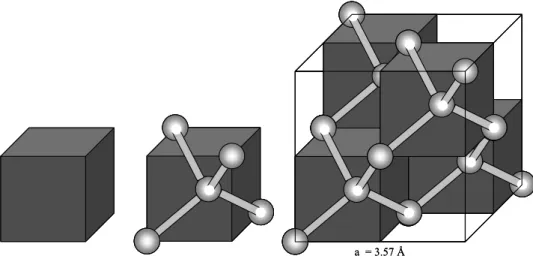
The diamond is constituted of carbon atoms in a tetrahedral lattice and is classified in crystallography as face cubic centered (fcc), the same as silicon. In particular, to any lattice point, a primitive base of two carbon atoms arranged in the (0,0,0) and (1/4,1/4,1/4) position is associated. The carbon atoms are hybridized sp3, anyone of them form four covalent bonds with the four nearest-neighbor, as illustrated in Fig. 2.1.
a = 3.57 Å a = 3.57 Å
Fig. 2.1 Crystalline structure of diamond obtained by repetition of blocks tetrahedrally
connected. The first neighbor define four faces of a cube, the cubs are grouped to make a cubic structure. In particular, it is reported the reticular constant a = 3.57 Å.
The nearest-neighbor distance is 1.54 Å, which is almost half of that of silicon. Because of that, diamond presents a remarkable lightness but a very compact structure, which confers a very interesting series of mechanical, thermal and chemical properties for a large number of applications.
Natural diamond is monochrystalline and depending of the nitrogen content and the form that it is placed in the crystal (substitutional, aggregate, etc.) it is classified according to the following scheme: type IA, IIA, IB and IIB. Type IA is the most abundant in nature and contents approximately 0.1% of nitrogen in the form of small aggregates; type IB contents nitrogen as interstitial impurity and almost all artificial diamond grown at high
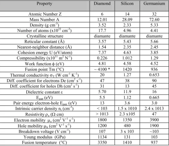
pressure and high temperatures are of this type. Types IIA and IIB are very rare in nature and are characterized by extremely low nitrogen concentrations. In particular, IIA diamond presents optical and thermal qualities superior to other types, while type IIB presents optimal properties as semiconductor and it’s of blue color. The main atomic, crystallographic, thermal and electrical properties of diamond are listed in Table 2.1, where are compared with that of silicon and germanium.
Table 2.1 Fundamental properties for diamond, silicon and germanium at 300 K.
Property Diamond Silicon Germanium
Atomic Number Z 6 14 32
Mass Number A 12.01 28.09 72.60
Density (g cm-3) 3.52 2.33 5.33
Number of atoms (x1022 cm-3) 17.7 4.96 4.41
Crystalline structure diamante diamante diamante
Reticular constant (Å) 3.57 5.43 5.66
Nearest-neighbor distance (Å) 1.54 2.35 2.45
Cohesion energy U (eV/atom) 7.37 4.63 3.85
Compressibility (x1011 m2 N-1) 0.226 1.012 1.29
Work function φ (eV) 4.81 4.58 4.52
Fusion point Tm (°C) ~ 4100 * 1420 936
Thermal conductivity σT (W cm-1 K-1) 20 1.27 0.653
Diff. coefficient for electrons De (cm2 s-1) 47 38 90
Diff. coefficient for holes Dh (cm2 s-1) 31 13 45
Dielectric constant ε 5.70 11.9 16
Egap (eV) 5.5 1.12 0.665
Pair energy electron-hole Epair (eV) 13 3.6 3.0
Intrinsic carrier density ni (cm-3) < 103 1.5 x 10¹⁰ 2.4 x 10¹³
Resistivity ρe (Ω cm) > 1013 2.3 x10⁵ 47
Electron mobility µe (cm2 V-1 s-1) 1800 1350 3900
Hole mobility µh (cm2 V-1 s-1) 1200 480 1900
Breakdown voltage (V cm-1) 107 3 x 10³ ~103
Young modulus (GPa) 1134 131 103
Fusion temperature (°C) 3350 1410 937
* Carbon graphitization it’s produced at 700 °C in presence of Oxygen.
2.2.1 Resistance to harsh environments
A fundamental aspect of diamond is his resistance to harsh environments. For example, in relation to chemical agents, it is inert to any chemical attack until the temperature of 900 °C, while for higher temperatures until the fusion temperature (3350 °C
at atmospheric pressure [19]) reacts in practice only with oxygen. The high fusion point represents another interesting aspect of diamond, allowing the engagement at high temperature environments. Diamond also shows a remarkable resistance to radiation of various types [20]; in particular, dose limits are always higher than then of silicon and it makes diamond attractive to operate in high intensity radiation fields.
2.2.2 Mechanical properties
Diamond is often used as abrasive in mechanical work due to his exceptional hardness. In fact, monochrystalline diamond is the harder material in nature, supporting pressures until 9000 Kg/mm2. Moreover, diamond has the higher atomic density (1.77x1023 cm-3) at atmospheric pressure and a mass density of 3.52 gcm-3. Another important characteristic of diamond is that it has the higher known Young’s modulus (1134 GPa) that results practically independent from both, direction in which is measured [21] and temperature until 800 °C approximately [22].
2.2.3 Electronic properties
A direct consequence of the high compact lattice structure of diamond is the wide energetic separation (gap) between valence band and conduction band, which is near 5.5 eV. This gap is highly greater than that of silicon and allows considering pure diamond as insulator when it’s maintained at room temperature [19]. In particular, this high difference in energy between valence band and conduction band allows to operate diamond microsystems in temperatures highly greater than room temperature, till 600 °C, without notice about a signal saturation linked to the pass of a high number of electrons in conduction band. However, in the case of silicon, temperatures little higher than room temperature are enough to produce a saturated signal, then destroying the semiconductor
properties of the material and avoiding the device operation. The high value of the energy gap Egap confers to the diamond a high resistivity (ρ ~ 1015 Ωcm, in light absence), that
allows to produce intrinsic diamond devices, different to silicon, for which is necessary to make junctions to obtain the same result. Also the high breakdown field, 107 V/cm approximately, depends on the value of the Egap. In particular, the union between these
properties with thermal characteristics, which follow, allows obtaining microsystems that are able to absorb high power respects to their own dimensions. This is a remarkable advantage, because high power dissipation requires non-trivial volumes. It is known that in presence of an opportune doping element diamond shows piezoresistive properties [23], useful to project a microsystem apt for electromechanical measurements (pressure, acceleration), also operating at high temperatures [24].
2.2.4 Thermal properties
Thermal conductivity of diamond is about 20 W/cm K and results 5 times greater than that of cupper and comparable with that of materials as lithium fluoride (LiF) and aluminum oxide (Al2O3). This good thermal conductivity is very important for the
mechanical elaboration, where is necessary to rapidly transfer the heat produced by the elaboration. We observe that high thermal conductivity seems to contrast with the fact that at room temperature diamond is practically an insulator. The point is that the particular diamond structure, extremely compact, joined to the lightness of carbon atoms from which it’s formed, made extremely easy phonon transport in diamond, for which, in effect, heat transport depends on the phonons instead of electrons [25]. In particular, the possibility of heat dissipation while being an insulator made possible, at least in perspective, the elaboration of mixed systems diamond/silicon (diamond as we will see grows on diamond)
in which on the silicon are made the electronics or the microsystems, while diamond act as heat dissipator.
2.2.5 Optical properties
Also from the point of view of optical properties diamond shows very interesting characteristics. It is practically transparent to radiation, from far infrared to the ultraviolet, corresponding to the gap at 225 nm (5.5 eV). In particular, it’s observed weak transitions at two or three phonons in the 1332 – 2664 cm-1 and 2665 – 3994 cm-1 intervals, which represent the only zones of intrinsic absorption. Other types of absorptions must be imputed to the impurities [26]. This optimal transparency characteristic, together with that of resistance, make diamond an ideal material for the production of optical windows for power lasers or connect optically harsh environments [22].
2.3 DIAMOND GROWTH
Diamond properties just reported allow to understand how could be important the application of this material in many fields. In the other hand, at it’s known, natural diamond besides being little abundant in nature could be also very expensive (if we think in IIB type) and it’s presented as monochrystalline type which geometries and dimensions are difficult to practical use. So, it was necessary to study production techniques of artificial diamond in order to obtain this material easy to use for microsystems production and with the possibility of modifying some specific properties only varying in the right way the growth process parameters. Then, it is presented the most common production techniques for diamond, both, monochrystalline, that is based in the engagement of high pressures and high temperatures, and polycrystalline, that use low pressure methods. We
note that in the first case the growth occurs in the region of the phase diagram of carbon, illustrated in Fig 2.2, for which diamond is in the stable state, while in the second case diamond grows, at smaller pressures, in the region where graphite is in the stable state and diamond in the metastable state [27].
Fig. 2.2 Phase diagram of carbon. Regions of metastable diamond and graphite are limited
by dot lines, that are extensions of the lines that separate diamond and graphite stable from liquid phase.
2.4 HIGH PRESSURE AND HIGH TEMPERATURE (HPHT) GROWTH
METHOD
This method is similar to the natural formation of diamond monocrystals; it means a high pressure (60 GPa approximately) and high temperature (till 1600 °C) environment for diamond growing from carbon. In the laboratory it is used the knowledge of the carbon phase diagram (Fig. 2.2) and graphite as base material. Nowadays with the HPHT [28] technique the biggest diamond crystals are produced (till some cubic millimeters), but are characterized for a high impurity level, irreducible in this growth conditions. This doesn’t limit the use in the microsystems field, for which mechanical elaboration represents the
main application field for this type of artificial diamond, but with production costs non-trivial, for which sometimes the use of natural diamond is more convenient.
2.5 LOW PRESSURE GROWTH METHODS
The introduction of low pressure methods allowed enormous progress in artificial diamond synthesis [29-31], for which the study and use of this methods is at the present very diffused and we can say that today artificial diamond growth with these methods presents many properties similar to those of natural diamond. In the low pressure methods diamond is deposited with the Chemical Vapor Deposition (CVD) technique. In particular, carbon is supplied as an opportune chemical composed (for ex: CH4) in gas or vapor
phase. Carbon is then chosen supplying energy to the gas in order to divide the molecule in which the gas is fixed. This could be obtain by heating or with radio frequency, and the use of a technique instead another, as well as the chose of the gas mix in gas or vapor phase, differentiates between the different available techniques for CVD diamond growth.
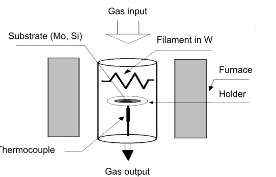
2.5.1 Hot filament method
In this method (Hot Filament Chemical Vapor Deposition or HFCVD), the general scheme is reported in Fig. 2.3 [32], the necessary energy for diamond deposition is provided by a hot metal filament (generally made of tungsten) placed some millimeters from substrate (made of silicon or molybdenum) where will take place diamond deposition [33]. In particular, the filament is electrically heated till 2000 °C approximately, while the deposition chamber is maintained at 700 – 1000 °C. The inlet gas mix is composed by methane (1% in volume) and hydrogen, diluted in nitrogen. The chamber pressure is maintained in the 1 – 10 KPa interval.
Holder Furnace Filament in W
Gas output Thermocouple
Substrate (Mo, Si)
Gas input
Fig. 2.3 General scheme of a hot filament deposition apparatus.
The HFCVD method is in principle very simple and economic and is surely the most diffuse. The most interesting aspect of this technique is represented by the flexibility in form and dimensions of the films that could be deposited. Moreover, the deposition rate is similar to others CVD techniques, being in the 0.1 – 1 µm/h interval. However, between the problems related with this technique must be noted the high impurity concentration and a low stability of the deposition process.
2.5.2 Combustion flame deposition
The Combustion Flame Deposition (CFD) owes his name to the fact that the necessary excitation energy for diamond growth is supplied by a flame generated from the combustion of a hydrocarbon gas (typically acetylene) with oxygen [34]. In particular, the growth substrate, mounted on an appropriate sample holder, is exposed directly to the flame and water cooled, as illustrated in Fig. 2.4.
INNER FLAME ACETYLENE FEATHER WATER COOLING OUTER FLAME OUTER FLAME INNER FLAME ACETYLENE FEATHER WATER COOLING OUTER FLAME OUTER FLAME
Fig 2.4 General scheme of a combustion flame deposition apparatus.
This method is very simple and presents high growth rates (till 50 µm/h); however, the quality of the obtained diamond, specially for optical, electronic and purity characteristics, cannot be compared with that obtained by hot filament nor that obtained by plasma enhanced deposition, which follows. Nevertheless, diamond obtained by CFD method maintains good thermal and mechanical properties that make it appropriate for instruments coating for mechanical work.
2.5.3 Plasma jet deposition
The Plasma Jet Deposition (PJD) is a technique that use a plasma to supply the necessary energy to the diamond growth [35]. The substrate is placed at the exit of a plasma source, in a vacuum environment (10 KPa approximately). The typical used gases are hydrocarbons with the addition of hydrogen. In particular, the use of oxygen could improve the quality of the produced films. The general scheme of some PJD deposition systems for diamond is illustrated in Fig. 2.5.
DC Supply RF Supply Substrate Substrate Substrate Gas Inlet Gas Inlet Gas Inlet Microwave Cavity DC Supply RF Supply Substrate Substrate Substrate Gas Inlet Gas Inlet Gas Inlet Microwave Cavity
Fig 2.5 General scheme of a plasma jet deposition apparatus.
The PJD presents a high growth rate (till 100 µm/h) and the quality of the films produced are superior to those obtained by combustion flame deposition, above all for optical properties. Problems become when it is intended to obtain homogeneous areas superior to 1 cm2.
2.5.4 Plasma enhanced deposition
Microwave Plasma Enhanced Chemical Vapor Deposition (MPECVD) [35,36] is
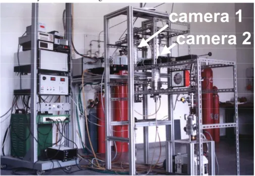
characterized by the high purity of produced films and then particularly interesting for microsystems production, even though, for problems related to the power density of the plasma, it’s not appropriated for large areas production (> 100 cm2) and could not be applied for non-planar areas production. The main idea is to use a plasma to supply the necessary energy for the activation of the chemical deposition of the vapor phase and in general microwaves at 915 MHz or 2.45 GHz are used. A typical reactor for plasma enhanced CVD diamond growth is illustrated in Fig. 2.6 and is referred to the apparatus that is used at the Mechanical Engineering Department of the University of Rome “Tor Vergata” laboratories [37,38].
MICROWAVE GENERATOR 2.45 GHZ MICROWAVE POWER SUBSTRATE TEMPERATURE GAS IN FLOW CONTROLLERS SAMPLE TO PUMP OPTICAL PYROMETER PRESSURE CONTROL PLUNGER QUARTZ TUBE QUARTZ WINDOW MICROWAVE GENERATOR 2.45 GHZ MICROWAVE GENERATOR 2.45 GHZ MICROWAVE POWER SUBSTRATE TEMPERATURE GAS IN FLOW CONTROLLERS GAS IN FLOW CONTROLLERS SAMPLE TO PUMP OPTICAL PYROMETER OPTICAL PYROMETER PRESSURE CONTROL PRESSURE CONTROL PLUNGER PLUNGER QUARTZ TUBE QUARTZ TUBE QUARTZ WINDOW QUARTZ WINDOW
Fig. 2.6 General scheme of the apparatus used in the present work for
CVD diamond films deposition.
It is constituted of a vacuum chamber, with gas flow controllers, inside which is a sample holder made of steel, water cooled, on which is placed the silicon substrate where diamond will grow. Microwaves, generated by a magnetron at 2.45 GHz, are propagated within the chamber (which acts as a resonant cavity) through a waveguide. Microwaves yield its energy to the plasma electrons, which at his time yield the energy to the gas through collisions and then heating it [39]. The chemical reactions, which follow the heating, move towards the formation, between others composed, of carbon, which is then deposited on the silicon substrate, giving place to a diamond film growth. It’s worth underline that diamond growth is obtained only if on the substrate surface are present nucleation centers (obtained by a pre-treatment of the substrate) and growth parameters (gas composition, pressure, plasma temperature, microwave power density, etc) are chosen in the appropriate way. In particular, the grow rate of diamond with this method vary from 0.2 µm/h to 10 µm/h, depending on growth parameters and chamber geometry.
2.6 CVD DIAMOND FILMS PRODUCTION
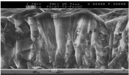
We’ve seen a typical scheme of a PECVD diamond film reactor (Fig. 2.6) and in particular we referred the diamond film deposition apparatus used for the present work. In this type of reactor, microwaves give energy to the electrons of the plasma, which, at his time, give energy to the gas through molecular collisions, heating it. The chemical reactions, which follow this heating, allow the formation of carbon that is deposited on the silicon substrate. The various monocrystals derived from the nucleation centers grow till make a continuous film. In particular, when growth goes on, some crystals are “submerged” from others called “dominants” and grains are always bigger. This gives, as a result, the typical columnar structure for diamond films, as it is clearly shown if we look a polycrystalline diamond film in section through a scanning electronic microscope (SEM) (Fig. 2.7).
Fig. 2.7 Cross section of a polycrystalline diamond film seen at the Scanning Electron
Microscope (SEM).
2.6.1 CVD diamond growth and nucleation
It is appropriate to notice that diamond growth occurs only if the substrate surface is the opportune one, it means if we’re in presence of nucleation centers. With this purpose, the silicon substrate is pre-treated in order to favor diamond nucleation. In
general, this pre-treatment is made through a technique called “scratching”, which consists in submerging the silicon substrate in an ultrasonic apparatus in which is contained an abrasive solution (typically micrometric diamond dust in acetone). The collision of abrasive particles produce on the substrate surface micro-scratches, which represent the nucleation centers. Alternatively it could be used the “biasing” technique, it consists in produce the nucleation centers directly on the silicon substrate placed in the vacuum chamber. In practice, in plasma presence, a potential difference of hundred of volts is applied in order to generate a high flux of plasma ions to the substrate. The collision of these ions on the silicon surface produces micro-scratches that remarkably increase the nucleation.
Once created the nucleation centers, the diamond growth could be done. It is worth notice that in low pressure methods the growth is obtained in the steady state of graphite in the phase diagram of carbon, while diamond is unsteady. Therefore, in order to allow diamond growth it’s necessary to create a formation barrier to the graphite and this is the role of the hydrogen in the growth process. In fact, most accepted theories [40] assume that is a simultaneous deposition of hybridized carbon sp3 (diamante) and sp2 (graphite). The formation of diamond is facilitated by the presence of hydrogen because it’s placed on the film surface reacting with the free bond of the carbon from the hybridization sp2 [41]; by this way it’s formed on the diamond surface an uniform saturated hydrocarbon layer that inhibits the single atom species to be deposited on the surface. So, hydrogen presence must suppress nucleation and growth of unsaturated graphitic structures. In fact, it’s noted that the presence of molecular hydrogen diminishes dramatically spontaneous nucleation and graphite deposition. Nevertheless, only molecular hydrogen cannot full suppress graphite growth: graphitic carbon can; in fact, nucleate on the diamond surface and ulterior
suppress the same diamond growth. Then, it is necessary to remove graphitic deposits using atomic hydrogen.
2.6.2 C/H/O Diagram
Theory and experience show that the choose of gas mix and his purity play a fundamental role in the produced diamond quality and in its growth rate. As it was told, the chemical species to be used are essentially carbon and hydrogen; the presence of oxygen could bring the increment of the growth rate. In particular, the concentration of the gases to be used for diamond growth could be visualized through a ternary diagram proposed by Bachmann [42] and shown in Fig. 2.8.
non diamond carbon growth region
no growth region H/(H+C ) C/ (C +O ) O/(O+H) C H Dia O mond dom ain 0.1 0.9 C2H2 CO 0.1 C2H4 C2H6 CH4 CO2 0.9 0.1 0.9 non diamond carbon growth region
no growth region H/(H+C ) C/ (C +O ) O/(O+H) C H Dia O mond dom ain 0.1 0.9 C2H2 CO 0.1 C2H4 C2H6 CH4 CO2 0.9 0.1 0.9
Fig. 2.8 Ternary diagram of gas concentration present in the growth chamber (Bachmann’s
diagram).
The diagram is a triangle in which any side reports the relative concentration of the three atomic species C, H and O generally present in the gas mix used for diamond growth. In particular, three regions are distinguished: a region of no growth, a graphite growth region but non-diamond and a diamond growth region. As is evident, the last one is closed
between the first two, that are preponderates. The diagram clearly shows how diamond could be obtain even in absence of oxygen. In this case, the most used gas mix is composed of little quantities of methane in hydrogen. However, it’s possible to obtain diamond also in presence of oxygen, but in this case growth is verified only if carbon concentration is lightly superior to that of oxygen, that’s because there is formation of CO and diamond is deposited only if sufficient carbon atoms remain. At the end, diagram reports the concentration lines of C, H and O for gas mix most common used (CO2 – CH4,
CO2 – C2H6, CO2 – C2H4, CO2 – C2H2).
It’s worth underline that a fundamental aspect to obtain good quality diamond is represented by the purity of the used gases. The presence of impurities in the gas mix allow their deposition and then to the formation of defects from various type and nature in the diamond crystal. To this purpose we notice that because CVD technique works at lower temperatures, diffusion and then concentration of polluting agents inside the crystal are lower than other production techniques of diamond.
We observed, as it was told before, diamond growth happens with the typical columnar structure and an interesting aspect of this type of growth is the growth rate dependence of the different crystallographic faces from growth parameters. In particular, it’s possible to vary the relative growth rate of various faces and then, controlling and acting on growth parameters (for ex: temperature or methane concentration [22]), it’s possible to favor some crystallographic orientations instead others and selecting, by this way, the characteristics of the desired film [43].
2.6.3 Optimization of growth parameters
The development and sharpening of the microwaves CVD technique at the Mechanical Engineering Department of the University of Rome “Tor Vergata” laboratories
and the characterization of obtained diamond films was discussed in three precedents PhD thesis [38,44]. In particular, growth parameters optimization studied in those works allowed to produce CVD diamond of excellent quality [45].
The present thesis is a natural continuation from precedents, emphasizing the reliability of the used growth technique, sample reproducibility and diamond doping.
In particular, during the PhD period, a new growth chamber was mounted, with the scope in deepening the knowledge acquired by the group in the last few years. The mounted apparatus is similar to that of Fig. 2.6. It’s composed by a tubular microwave CVD reactor, in which the growth chamber is constituted by a 60 mm quartz tube maintained in vacuum, microwaves are generated by a commercial magnetron of 2.45 GHz and a power of 2 KW. The silicon substrate (pre-treated with the scratching technique) is placed on a sample holder made of steel, in direct contact with the plasma, cooled by water. The substrate temperature (fixed in the 650 – 850 °C range) is continually measure through an optical infrared pyrometer and automatically controlled by a system ad-hoc, via software, which regulates, in retroactive way, the power of the magnetron in order to maintain constant the substrate temperature.
The gas flow is controlled by four flowmeters. It is worth notice that for the precedent growth chamber was used, through the time, different gas mix for purity and composition: CH4 – H2, CO2 – CH4 and CO2 – C2H6. In particular, a systematic study for the quality of
the produced film varying the methane concentration [44] had indicated as the optimal mix that of CH4 – H2 at 1% of methane, because of that it was chosen as the gas mix for
diamond growth in the new chamber.
It is important to underline that the new chamber has obtained immediately results of remarkable interest, allowing the realization of high quality diamond films, which made more promising future works in order to optimize growth parameters. Another important