A. Ronchi,1, 2, 3, ⇤ P. Franceschini,1, 2, 3 P. Homm,1 M. Gandolfi,4, 5 G. Ferrini,2, 3
S. Pagliara,2, 3 F. Banfi,6 M. Menghini,7, 1 J-.P. Locquet,1 and C. Giannetti2, 3, † 1Department of Physics and Astronomy, KU Leuven, Celestijnenlaan 200D, 3001 Leuven, Belgium 2Department of Mathematics and Physics, Università Cattolica del Sacro Cuore, Brescia I-25121, Italy
3ILAMP (Interdisciplinary Laboratories for Advanced Materials Physics), Università Cattolica del Sacro Cuore, Brescia I-25121, Italy
4CNR-INO, Via Branze 45, 25123 Brescia, Italy
5Department of Information Engineering, University of Brescia, Via Branze 38, 25123 Brescia, Italy 6Université de Lyon, Institut Lumière Matiére (iLM), Université Lyon 1 and CNRS,
10 rue Ada Byron, 69622 Villeurbanne Cedex, France 7IMDEA Nanociencia, Cantoblanco, 28049 Madrid, Spain
(Dated: April 14, 2021)
The insulator-to-metal transition in Mott insulators is the key mechanism for a novel class of electronic devices, belonging to the Mottronics family. Intense research efforts are currently devoted to the development of specific control protocols, usually based on the application of voltage, strain, pressure and light excitation. The ultimate goal is to achieve the complete control of the electronic phase transformation, with dramatic impact on the performance, for example, of resistive switching devices. Here, we investigate the simultaneous effect of external voltage and excitation by ultrashort light pulses on a single Mottronic device based on a V2O3epitaxial thin film. The experimental results, supported by finite-element simulations of the thermal problem, demonstrate that the combination of light excitation and external electrical bias drives a volatile resistivity drop which goes beyond the combined effect of laser and Joule heating. Our results impact on the development of protocols for the non-thermal control of the resistive switching transition in correlated materials.
I. INTRODUCTION
Mott insulators are a class of quantum materials exhibiting the most promising properties and functionalities for the next generation of solid-state devices belonging to the Mottronics family[1–4]. Correlated vanadium-oxides have been inten-sively studied due to the possibility of selectively controlling the resistive switching process at the core of resitive memories and neuromorphic computing[5–8]. The conventional route to control the resistive switching dynamics is based on the tuning of chemical doping[9–11], temperature [12, 13], pressure[14– 17], strain[18–20] and on the application of external electric fields[21–25]. More recently, the sudden excitation via ultra-short laser pulses[12, 26–33] has been introduced as a novel control parameter, although the nature of the photoinduced insulator-to-metal transition is still subject of intense debate. Much effort has been so far dedicated to the study of the tran-sient optical, electronic and lattice properties[12, 26–33] and on the role of intrinsic nanoscale inhomogeneities[12, 13, 34] with the goal of understanding to what extent the photoin-duced transition is similar to the thermally driven one. In contrast, little is known about the actual resistive state that is induced by light excitation possibly combined with external voltage. Recent theoretical works have suggested that, in the vicinity of the insulator-metal coexisting region, the applica-tion of voltage[23] and the excitaapplica-tion with light pulses capable of manipulating the band occupation[12, 35], can lead to the weakening of the insulating state and, eventually, to the com-plete collapse of the Mott insulating phase and the consequent
⇤[email protected]. †[email protected].
resistive switching along a non-thermal pathway.
Here we developed a Mottronic device, based on a micro-bridged V2O3epitaxial thin film, in which the resistance state
consequent to a controlled excitation by trains of ultrashort light pulses can be measured. V2O3 is a prototypical Mott
insulator that exhibits a first-order Insulator-to-Metal transi-tion (IMT) occurring at TIMT ⇠ 170 K and characterized by a
resistivity change of several orders of magnitude[14, 15, 17]. When a voltage larger than a temperature-dependent threshold DVth is applied in the insulating state (T < TIMT), the device
undergoes a resistive switching process, i.e. the resistance suddenly drops to the metallic value. However, the switch-ing process in V2O3devices is associated to the formation of
micrometric conductive filaments[25], which usually makes the evaluation of the local heating and the investigation of the thermal nature of the dynamics rather difficult. In order to avoid this additional complexity, we investigate the light in-duced volatile resistance drop for different applied voltages, always smaller than DVth. This below-threshold resistance
drop thus provides information about the weakening of the insulating phase, triggered by the combined voltage-light ex-citation, while avoiding the formation of the conductive chan-nels associated to the resistive switching process. Starting from the resistance vs temperature calibration curve of the de-vice, we are able to compare the photoinduced resistivity drop to the local heating effect, which is carefully estimated by finite-element simulations. Our main results can be summa-rized as follows. The application of a sufficiently long train of light pulses alone drives a volatile resistance drop that is com-patible with that predicted by finite-element simulations of the thermal problem. The minimum number of pulses necessary to observe a significant effect suggests that the light-induced local heating is mediated by the electronic specific heat, which
becomes extremely large as TIMTis approached. Furthermore,
when a significant below-threshold electrical bias (DV=0.5 V) is applied, the light-induced volatile drop of the resistance is twice than what is expected by considering both the laser-induced and Joule heating. This result leads to the conclu-sion that the combined voltage-light excitation protocol makes the system more fragile towards the collapse of the insulating electronic phase.
II. METHODS A. Mottronic device
An epitaxial V2O3 film with thickness d=67 nm is
de-posited by oxygen-assisted molecular beam epitaxy (MBE) in a vacuum chamber with a base pressure of 10 9Torr. A 37
nm Cr2O3buffer layer is interposed between the film and the
substrate to minimise lattice mismatch and optimise strain re-laxation in the film. A (0001)-Al2O3substrate is used without
prior cleaning and is slowly heated to a growth temperature of 700 °C. Vanadium is evaporated from an electron gun with a deposition rate of 0.1 Ås 1, and an oxygen partial pressure
of 6.2 · 10 6Torr is used during the growth [18]. Under these
conditions, a single crystalline film with the c-axis oriented perpendicular to the surface is obtained. A micro bridge, con-stituted by 40 nm Au/5 nm Ti thick electrodes with w=50µm width and s=2 µm separation, is nanopatterned on the film surface, as shown in Fig. 1a. Temperature-dependent resistiv-ity measurements (see Fig. 1b) are performed using a Keithley Sourcemeter 2634B in the 2-points configuration across the Au/Ti electrodes. The device temperature is controlled by a closed cycle cryostat equipped with a heater. The temperature sweep rate is set to 0.5 K per minute. When cooled down, the device undergoes the metal-to-insulator transition, character-ized by a resistance increase of almost three order of magni-tudes. In our device the resistance ranges from 20W at room temperature (metallic state) to 130 kW at T=140 K (insulating state). The heating and cooling branches evidence the typical hysteresis cycle of the IMT, which spans the insulator/metal coexistence region from 155 to 185 K. In the following, we will consider TIMT '170 K as the temperature corresponding
to the midpoint of the heating branch of the hysteresis cycle.
B. Photo-induced resistance drop measurements
Resistance measurements are combined with light excita-tion by focusing a train of infrared pulses (0.4µJ, 50 fs) at 800 nm wavelength (1.55 eV photon energy) generated by an optical parametric amplifier pumped by an Yb-laser system. A pulse picker allows to control both the repetition rate, set to 25 kHz, and the total number of pulses impinging on the sample. The laser output is focused on the device by a 10 cm lens. The Full-Width-Half-Maximum (FWHM) of the spot size on the device is 50µm, as measured using the knife-edge technique. The pump incident fluence on the device is of the order of 0.2 mJ/cm2, which is below the threshold necessary
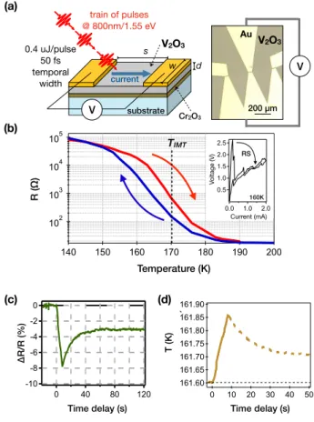
train of pulses @ 800nm/1.55 eV 0.4 uJ/pulse 50 fs temporal width V2O3 substrate Cr 2O3 V (a) 200 µm (b) (d) Time delay (s) T (K) 161.90 161.85 161.80 161.75 161.70 161.65 161.60 50 40 30 20 10 0 (c) -10 -8 -6 -4 -2 0 120 80 40 0 Δ R/R (%) Time delay (s) Au V 2O3 V current d w s R ( Ω ) Temperature (K) 102 103 104 105 200 190 180 170 160 150 140 TIMT 2.5 2.0 1.5 1.0 0.5 2.0 1.0 0.0 Voltage (V) Current (mA) RS 160K
FIG. 1. Working principle of the experiment. (a) Left: Cartoon of the experimental set-up. A finite train of laser pulses (¯hw = 1.55 eV, 50 fs temporal width,n = 25 kHz) is used to photoexcite the device. The change in the 2-points resistance of the device is simul-taneously measured before, during and after the laser excitation by means of Au/Ti electrodes. The contact resistance can be neglected since is very small (⇠ 5 W) with respect to the V2O3bridge resis-tance (⇠ 15 kW). Right: Microscopic image of the device used dur-ing the experiment. (b) Equilibrium 2-points resistance hysteresis measured as function of the temperature. The red (blue) arrows indi-cate the heating (cooling) branch. Inset: 2-points I-V curve showing volatile resistive switching at T =160 K. The measurement has been performed through the 2 µm gap shown in (a). (c) Relative vari-ation of resistance measured across the device as a function of the time delay at the base temperature T0=161.6 K. The time zero corre-sponds to the moment when the first pulse of the laser train arrives. (d) Result of the conversion of resistance drop measurements (see panel (c)) into effective local temperature (yellow solid line). The resistance vs temperature curve shown in Fig.1(b) has been inverted to obtain, for each value of resistance, the corresponding local tem-perature. As explained in the main text, the cooling down process takes place along a resistance-temperature curve which differs from the equilibrium one reported in panel (b). The dashed line, corre-sponding to the cooling down dynamics of the system, is the hypo-thetical local temperature obtained from the heating branch of the equilibrium resistance-temperature curve, but does not necessarily represents the actual local effective temperature of the system.
to photoinduce the complete insulator-to-metal transition[12]. In Fig. 1c we show the typical resistance drop measured af-ter excitation with a controlled number of light pulses (200 kpulses at 25 kHz rep. rate). Prior to the experiment the de-vice is cooled down to 100 K and then heated up to T '160 K, i.e. in the insulator-metal coexistence region. Before light excitation, the system is thus in a high resistivity state along the heating branch of the hysteresis curve shown in Fig. 1b. Laser excitation is then switched on and the time-dependent resistance is obtained by measuring the current flowing across the bridge at a fixed applied voltage (DV=5 mV) and at the nominal temperature T =160 K. After 8 s, i.e. at the end of the pulse train, the resistance drops by 8 % with respect to the initial value. Once the light excitation is removed, the rela-tive resistance variation, i.e. DR/R, starts to decrease, until it reaches a plateau corresponding to a non-volatile change of about 3%. The explanation of this effect resides in the inher-ent hysteresis of the IMT (see Fig.1 b): after the laser-induced warming up, which is not enough to drive the system out of the hysteresis region, the cooling-down takes place along a curve located somewhere between the complete warming up and cooling down curves (red and blue curves in Fig. 1b). The final resistance value is therefore smaller than the initial value, although the initial temperature is recovered. In order to restore the initial resistance value, the device must undergo a complete thermal cycle, corresponding to heating up to 300 K, followed by cooling down to 100 K and further heating up to T '160 K. The same thermal cycle protocol is applied be-fore any of the resistance drop measurements reported in the following.
The resistance-temperature curve shown in Fig.1b can be used to retrieve the precise local effective temperature of the V2O3device during the light excitation process, as shown in
Fig. 1d. The local effective temperature during the resistance drop is extracted by interpolating and inverting the heating branch of the resistance-temperature curve (Fig. 1b). The er-ror associated to the local effective temperature is obtained by considering the accuracy of the Keithley Sourcemeter (± 0.02 %) in the voltage range used during the experiments. We stress that the resistance-temperature relation is single-valued only along the heating branch. Therefore, the resistance value can be converted in the actual local temperature only during the heating up process in the 0-8 s time span. During the cool-ing down (8-120 ps) the resistance moves back along a non-equilibrium resistance-temperature curve, which differs from that used for calibration (Fig. 1b) and cannot therefore be used to retrieve the actual local temperature.
C. Finite Elements Method simulation of the thermal problem
The heating induced by the laser excitation is numerically simulated by finite-element methods (Comsol Multiphysics). In the simulations we consider the 67 nm thick V2O3film on
top of a 500µm thick (0001)-Al2O3 substrate. The Cr2O3
buffer-layer is omitted since its thermal and optical properties are very similar to the sapphire’s ones. The problem is solved in 2D axial symmetry in a region with 800µm diameter. A
Time (s)
Temperatur
e (K)
(a)
260 240 220 200 180 160 10-14 10-12 10-10 10-8 10-6 10-4 162.1 162.0 161.9 161.8 161.7 161.6 10-5 10-3 10-1 101(b)
Temperatur
e (K)
Time (s)
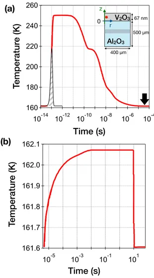
V2O3 Al2O3 400 µm 500 µm 67 nm z r 0FIG. 2. Finite elements method simulations. (a) The solid line represents the temperature increase due to the single pulse excitation (black dashed area) as function of the time (logarithmic scale). The black arrow indicates the instant (t = 40µs) at which the following pulse arrives. Inset: sketch of the geometry used in the Comsol sim-ulations. The red dot indicates the point at which the temperature has been evaluated (r = 50 nm; z=33.5 nm). (b) The temperature variation at saturation, induced by 2 · 105laser pulses, is shown. The temperature is evaluated at half of the total thickness, i.e. r = 50 nm and z=33.5 nm. The maximum temperature reached after the excita-tion with the pulse train is used as input to build the curves reported in Fig. 3.
representation of the sample cross section is reported in the inset of Fig. 2a. Thermal insulating boundary conditions are applied on the top and lateral boundaries, whereas the sap-phire bottom boundary (z = 500µm) is kept at the constant temperature T0=161.6 K, which corresponds to the actual
initial effective temperature of the device, as extracted from the resistance value.
The thermal problem for single pulse excitation is initially addressed. In this configuration, a single pulse with temporal
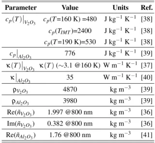
TABLE I. Summary of materials parameters values adopted in the present work for FEM simulations.
Parameter Value Units Ref.
cp(T )V2O3 cp(T =160 K) =480 J kg 1K 1 [38] cp(TIMT)=2400 J kg 1K 1 [38] cp(T =190 K)=530 J kg 1K 1 [38] cp Al 2O3 776 J kg 1K 1 [39] k(T)V2O3 k(T) (⇠3.1 @160 K) W m 1K 1 [37] k Al2O3 35 W m 1K 1 [40] rV2O3 4870 kg m 3 [39] rAl2O3 3980 kg m 3 [39] Re( ˜nV2O3) 1.997 @800 nm kg m 3 [36] Im( ˜nV2O3) 0.382 @800 nm kg m 3 [36] Re( ˜nAl2O3) 1.76 @800 nm kg m 3 [41]
and spatial gaussian profiles matching the experimental ones, excites the sample. We consider an energy density delivered to the system (0.66 kJ/cm3) such that the time and spatial
integral matches the total energy released by the laser pulse upon accounting for reflection losses. The estimated energy absorbed within the 67 nm V2O3film is calculated with a
mul-tireflection model (total absorption A= 0.22), assuming the op-tical constants reported in the literature[36]. Using Fourier’s law, the energy balance within the volume of the V2O3 film
reads:
— ·⇥ k(T(r,z,t))—T(r,z,t)⇤+
+P(r,z,t) =r cp((r,z,t))∂T(r,z,t)∂t (1)
where P(r,z,t) is the absorbed pulsed power density profile, k(T) is the temperature dependent thermal conductivity[37], r the mass density, and cp(T ) the temperature-dependent total
specific heat at constant pressure[38]. For sake of complete-ness, the parameters used in the simulation are reported in Ta-ble I. The following heat flux continuity boundary condition is used at the V2O3/ Al2O3interface:
kV2O3 ∂T ∂z z=0+ =kAl2O3 ∂T ∂z z=0 . (2)
The initial condition is T0=161.6 K throughout the sample
and the substrate. The equation is solved via the finite el-ement method, covering a time scale spanning seven orders of magnitude. Since the presence of a thermal boundary re-sistance (TBR) at the V2O3/ Al2O3 interface can affect the
temperature of the V2O3film, simulations with different TBR
values were performed. Assuming a TBR (10 7 m2KW 1)
one order of magnitude larger than typical values reported for
similar materials[42], leads to a correction of the V2O3
tem-perature profile smaller than 10%, i.e. within the experimental uncertainty. The thermal dynamics of the single pulse excita-tion is shown in Fig. 2a. We remark that we are interested in thermal dynamics on timescales longer than the pulse du-ration and electron-phonon coupling. Therefore, we assume the complete thermalization between the electron and lattice subsystems, as implied by the use of the total specific heat and thermal conductivity values.
After the impulsive energy absorption, the temperature reaches its maximum value (⇠ 250 K) within few picosec-onds. Subsequently, the energy diffusion through the sapphire substrate drives the slower cooling down process. If we con-sider the time needed to reduce the initial temperature varia-tion by a factor 2, we obtain a half-life of about 2 ns. The cooling down to the initial temperature T0=161.6 K is almost
completed within ⇠ 40 µs, although a small temperature in-crease ⇠ 0.04 K persists. The simulations also demonstrate that, in the device region, the temperature variation within the V2O3 film is rather homogeneous, with less than 1%
differ-ence between the top and bottom temperatures. For sake of simplicity, in the following we will refer to the temperature of the point at 33.5 nm distance from the device surface (see Fig. 2a).
In the multi-pulse experimental configuration, the heating associated to each pulse accumulates on top of the tempera-ture increase triggered by the previous ones. Considering a pulse distance of 40 µs (25 kHz rep. rate), the small tem-perature difference accumulated after each pulse leads to a progressive increase of the local effective temperature, until the external heat flux is balanced by the dissipation. In this condition, the average effective temperature does not further increase and it reaches a saturation value, which ultimately drives the resistance drop across the bridge observed after the light excitation. For simplicity, the effect of the total thermal heating induced by the multi-pulse excitation is simulated by considering a laser beam with step-like temporal profile ex-tending over the same time span of the pulse train and with the same average power [40, 43, 44]. An example of the tem-perature dynamics, for a train of 2·105pulses, is shown in Fig.
2b. The heat accumulation leads, at saturation, to a final tem-perature of 162.1 K. The discrepancy between this value and the experimental one (see Fig. 2b) will be clarified in the next section. Once the input power is removed, the system rapidly cools down to the initial temperature. For a better comparison with the experimental data, the time-dependent temperature curves obtained by the simulations and reported in Fig. 2b were subsequently filtered by a low-pass filter with a band-width corresponding to the cut-off frequency (10 Hz) of the electrical circuit used for the resistance measurements.
III. RESULTS AND DISCUSSION
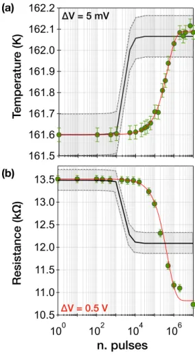
The comparison between the experimental results and the numerical simulations is shown in Fig. 3a. The applied volt-age for the resistance measurements isDV=5 mV, i.e. much smaller than the thresholdDVth'2.5 V necessary to obtain the
resistive switching at the working temperature. The experi-mental points (green circles) represent the maximum effective temperature increase, estimated by the volatile resistance drop described in Sec II B, as a function of the number of excita-tion pulses. We stress that each experimental point is obtained after a complete thermal cycle, necessary to restore the ini-tial resistance of the device (see Sec. II A). The data show that no significant temperature increase is detectable below ⇠ 104pulses. Above this threshold the temperature increases and saturates after approximately 106pulses. The temperature
achieved in the saturation regime, i.e. when the excitation av-erage power matches the thermal losses towards the substrate, is ⇠ 162.06 K.
On general grounds, the dynamics of the V2O3temperature
T (t) can be described in terms of a simple lumped-element model:
Ctd(T Tdt 0)=W R1
th(T T0) (3)
where T0=161.6 K is the initial temperature, Ct represents
the total heat capacity of the device, W is the total absorbed power, Rthis a constant with the dimensions of a thermal
re-sistance and effectively accounts for the total heat dissipation. Independently of the specific values of the effective coeffi-cients entering in the lumped-element model, the general so-lution of Eq. 3 is the exponential function T (t)=T0+dTsat
(1-e t/t), wheret=RthCt is the time constant of the heating up
process anddTsat=RthW is the temperature variation at
sat-uration. This exponential function can be used to fit the data and retrieve the experimental time constant of the system. The red solid line in Fig. 3a is the exponential fit, which provides t=18.5±0.8 s corresponding to (4.6±0.2)⇥105pulses.
The local effective temperature retrieved by the resistance drop is compared to the results of calculations of the full ther-mal problem, as described in Sec. II C. The black solid line in Fig. 3a represents the saturation temperature increase ob-tained by finite-element calculations, when an average power corresponding to that of the pulse train exciting the device is considered. The calculated saturation temperature increase, i.e. dTsat=0.5 K perfectly matches the experimental value.
Considering thatdTsat depends only on the adsorbed power
W and on Rth, we can conclude that the finite element
calcu-lations perfectly account for the heat dissipation, which is ul-timately regulated by the heat diffusion throughout the V2O3
film and the substrate.
The difference between the calculated and measured time constants of the exponential heating dynamics can be at-tributed to an underestimation of the total heat capacity Ct.
Throughout the calculations of the thermal problem, we as-sumed perfect electron-phonon thermalization and we have thus considered the V2O3 temperature-dependent total
spe-cific heat [38]. Nonetheless, the absorption of each single light pulse is mediated by the electronic population which undergoes a large temperature increase. The effective elec-tronic temperature dynamically overcomes the Mott insulator-to-metal transition temperature TIMT, which is accompanied
by a divergence of the electronic effective mass m⇤.
Con-sidering that the electronic specific heat of an electron gas celµ m⇤3/2, the dynamical crossing of TIMT is naturally
ac-companied by a large increase of cel[38], which is
character-ized by a narrow cusp centered at TIMT (see Tab. I). In the
vicinity of the Mott transition, the electron gas thus behaves like a reservoir capable of absorbing a large quantity of energy but limiting the impulsive increase of the effective tempera-ture of the electron-phonon system. Our experimental results are compatible with cel=(30±6)⇥cp(TIMT)V2O3, which
sug-gests an effective mass increase of 10, perfectly compatible with what recently observed in VO2[45] and attributed to the
strong electronic correlations.
Once assessed the validity of the thermal model to eval-uate the laser induced heating in the saturation regime, we can compare the expected thermally induced resistance drop to what is actually measured when the laser pulses are com-bined to a voltage that is no longer negligible with respect toDVth. In Fig. 3b we report the resistance drop, measured
following the procedure previously described, withDV=0.5 V applied voltage. In this case, although the resistance drop is described by an exponential function (solid red line) with the same time constant (t=18.7±1.6 s), the value achieved in the saturation regime (dRsat'2.6 kW) is twice the value
mea-sured (dRsat'1.3 kW) for DV =5 mV.
The resistance drop measured under the applied bias DV=0.5 V is compared to the value expected by consider-ing the laser-induced heatconsider-ing (the parameters of the thermal calculations are the same than the previous low-voltage case) and also including the effect of Joule heating induced by the current flowing throughout the V2O3 bridge. We stress that
the voltage applied through the device is smaller than thresh-old value necessary for the resistive switching. Therefore, in this regime no metallic filaments[25], possibly responsible for large local Joule heating, are created and the system can be treated as homogeneous. The additional dissipated power can be thus written as:
DPJ=DV ⇥Iswd (4)
where DPJ is the power density dissipated by the electrical
current I flowing through the electrodes and swd is the device effective volume (see Fig. 1a).DPJis added to the total power
density P(r,z), provided by the pulse train, in Eq 1. The black solid line in Fig. 3b represents the result of the numerical sim-ulation converted in the expected resistance drop by means of the resistance vs temperature calibration curve (see Fig. 1b). We note that the Joule heating induced by the current is of the order of 2⇥10 5W and is negligible as compared to the
laser power, which amounts to ⇠ 10 2 W. As a conclusion,
the additional Joule heating does not account for the measured resistivity drop in the stationary regime, which is twice than that expected from heating alone.
The present results can be rationalized on the basis of re-cent theoretical work[23], which showed that in the insulator-metal coexistence region, the application of a significant elec-tric field is able to induce the non-thermal weakening of the Mott insulating phase via the formation of new metallic states
Temperatur
e (K)
(a) 162.2 162.1 162.0 161.9 161.8 161.7 161.6 161.5 100 102 104 106n. pulses
(b)Resistance (k
Ω
)
13.5 13.0 12.5 12.0 11.5 11.0 10.5 103 100 102 104 106 ΔV = 0.5 V ΔV = 5 mVFIG. 3. Comparison between experimental and numerical re-sults. (a) Maximum variation of the sample’s temperature induced by the laser pulses as function of the total number of pulses (green circles). The applied voltage isDV=5 mV. The solid black line rep-resents the simulated data where the maximum temperature has been extracted for each finite number of pulses. The grey area shows the error interval associated to the model assumptions and numerical ap-proximations. The red solid line represents the exponential fit to the experimental data.(b) Maximum laser-induced drop of the device re-sistance when a constant voltage biasDV=0.5 V is applied across the Au/Ti electrodes (green circles). The solid black line represents the outcome of numerical simulations, from which the expected resis-tance drop is retrieved from the local effective heating for each finite number of pulses. The dissipated power related to the Joule heating has been added to the power dissipated by the laser excitation. The grey areas show the error interval associated to the model assump-tions and numerical approximaassump-tions. The solid red line represents the exponential fit to the experimental data.
at the Fermi level with no counterpart at equilibrium. This mechanism is in sharp contrast with the conventional Zener tunneling mechanism that is usually invoked to describe the resistive switching dynamics. Interestingly, the state variable that characterizes the transition and controls the free energy of the system is the orbital polarization, defined as p=nepg
-na1g, where nepg is the occupation of the lowest energy V-3d epg orbitals and na1gis the occupation of the V-3d a1gorbitals. The Mott insulating phase is characterized by p=2, whereas the application of an electric field induces the formation of a metallic state with p=1.2-1.6 [23]. As recently shown[12], the excitation with infrared light pulses with 1.55 eV photon en-ergy can induce a further orbital polarization decrease of the order ofd p '-10 3 10 2, which in turns leads to a change
of 1.3-13 meV of the difference between the free energies of the insulating and metallic phases. The photo-induced change of the free energy difference largely overcomes the thermal effect, i.e. kBdT '50 µeV, thus inducing the growth of
al-ready existing metallic domains in the insulator-metal coex-istence region. The combination of below-threshold voltage and the excitation with infrared light pulses capable of mod-ifying the occupation of vanadium orbitals thus weakens the insulating state well beyond what can be ascribed to thermal effects. The scenario emerging from our results can be un-derstood also within the resistor network model [21], which is commonly adopted to describe the insulator-to-metal switch-ing dynamics. In this model, the physical system is divided in nanometric cells representing small regions, which are either in the insulating (high-resistance) or metallic (low-resistance) states. The combined action of voltage and laser excitation leads to a non-thermal increase of the number of the metal-lic cells, thus triggering the observed volatile resistance drop. Working with below-threshold voltage and with weak laser excitation avoids the creation of connected filamentary metal-lic paths which are responsible for the resistive switching pro-cess observed aboveDVth.
IV. CONCLUSIONS
In conclusion, we investigated the simultaneous action of a train of infrared light pulses and an external voltage on a Mottronic device based on V2O3, which undergoes an IMT
at TIMT '170 K. When the device is in the insulator-metal
coexisting region (T '160 K) and a 0.5 V voltage is applied across the device, the measured resistance drop induced by a pulse number exceeding 106is twice than that expected from
the simple local heating of the device. Our results suggest that although the 0.5 V applied voltage is below the threshold (DVth=2.5 V) necessary for inducing the complete and
irre-versible resistive switch, it brings the insulating phase close to the insulator-to-metal instability. The simultaneous weak excitation with a sufficient number of infrared pulses modifies the occupation of the vanadium 3d orbitals enough to trigger the non-thermal growth and proliferation of already existing metallic nodes, well beyond what can be ascribed to the total local heating induced by the laser/voltage combination. The present results also call for the development of time-resolved microscopy techniques to investigate the real time dynamics of the metallicity in Mottronics and resistive switching de-vices subject to the simultaneous application of electric fields and light pulses.
ACKNOWLEDGMENTS
C.G., A.R. and P.F. acknowledge Andrea Tognazzi for the support in the development of the experimental set-up. C.G. and A.R. acknowledge Dr. Alessandro Bau’ and Prof. Vitto-rio Ferrari (Information Engeenering Dept., Università degli Studi di Brescia) for the support given during the wirebond-ing of the device. We thank Frederik Ceyssens for his help with the fabrication of electrical contacts on the samples. C.G., A.R., P.F. acknowledge financial support from MIUR through the PRIN 2017 program (Prot. 20172H2SC4_005).
G.F., and C.G. acknowledge support from Università Cattolica del Sacro Cuore through D.1, D.2.2, and D.3.1 grants. F.B. acknowledges financial support from Université de Lyon in the frame of the IDEXLYON Project-Programme Investisse-ments d’Avenir (ANR-16-IDEX-0005) and from Université Claude Bernard Lyon 1 thorugh the BQR Accueil EC 2019 grant. P.H., M.M., and J.-P.L. acknowledge support from EU-H2020-ICT-2015 PHRESCO Project, Grant agreement No. 688579. P.H. acknowledges support from Becas Chile-CONICYT. M. G. acknowledges financial support from the CNR Joint Laboratories program 2019-2021.
[1] Yoshinori Tokura, Masashi Kawasaki, and Naoto Nagaosa. Emergent functions of quantum materials. Nature Physics, 13(11):1056–1068, September 2017.
[2] Zheng Yang, Changhyun Ko, and Shriram Ramanathan. Oxide electronics utilizing ultrafast metal-insulator transitions. An-nual Review of Materials Research, 41(1):337–367, 2011. [3] J. Zhang and R.D. Averitt. Dynamics and control in complex
transition metal oxides. Annual Review of Materials Research, 44(1):19–43, 2014.
[4] D. N. Basov, R. D. Averitt, and D. Hsieh. Towards properties on demand in quantum materials. Nature Materials, 16(11):1077– 1088, November 2017.
[5] Y. Zhou and S. Ramanathan. Mott memory and neuromorphic devices. Proceedings of the IEEE, 103(8):1289–1310, 2015. [6] Etienne Janod, Julien Tranchant, Benoit Corraze, Madec
Querré, Pablo Stoliar, Marcelo Rozenberg, Tristan Cren, Dim-itri Roditchev, Vinh Ta Phuoc, Marie-Paule Besland, and Lau-rent Cario. Resistive switching in mott insulators and correlated systems. Advanced Functional Materials, 25(40):6287–6305, 2015.
[7] Javier del Valle, Juan Gabriel Ramírez, Marcelo J. Rozenberg, and Ivan K. Schuller. Challenges in materials and devices for resistive-switching-based neuromorphic computing. Journal of Applied Physics, 124(21):211101, 2018.
[8] Pavel Salev, Javier del Valle, Yoav Kalcheim, and Ivan K. Schuller. Giant nonvolatile resistive switching in a mott oxide and ferroelectric hybrid. Proceedings of the National Academy of Sciences, 116(18):8798–8802, 2019.
[9] H. Kuwamoto, J. M. Honig, and J. Appel. Electrical properties of the (V1 – xCrx)2O3system. Phys. Rev. B, 22:2626–2636, Sep 1980.
[10] P. Homm, L. Dillemans, M. Menghini, B. Van Bilzen, P. Bakalov, C.-Y. Su, R. Lieten, M. Houssa, D. Nasr Esfahani, L. Covaci, F. M. Peeters, J. W. Seo, and J.-P. Locquet. collapse of the low temperature insulating state in cr-doped V2O3thin films.
[11] Javier del Valle, Yoav Kalcheim, Juan Trastoy, Aliaksei Char-nukha, Dimitri N. Basov, and Ivan K. Schuller. Electrically induced multiple metal-insulator transitions in oxide nanode-vices. Phys. Rev. Applied, 8:054041, Nov 2017.
[12] A. Ronchi, P. Homm, M. Menghini, P. Franceschini, F. Mac-cherozzi, F. Banfi, G. Ferrini, F. Cilento, F. Parmigiani, S. S. Dhesi, M. Fabrizio, J.-P. Locquet, and C. Giannetti. Early-stage dynamics of metallic droplets embedded in the nanotextured Mott insulating phase of V2O3. Phys. Rev. B, 100:075111, Aug 2019.
[13] A. S. McLeod, E. van Heumen, J. G. Ramirez, S. Wang, T. Saerbeck, S. Guenon, M. Goldflam, L. Anderegg, P. Kelly, A. Mueller, M. K. Liu, Ivan K. Schuller, and D. N. Basov. Nan-otextured phase coexistence in the correlated insulator V2O3. Nature Physics, 13(1):80–86, September 2016.
[14] D. B. McWhan, T. M. Rice, and J. P. Remeika. Mott transition in Cr-doped V2O3. Phys. Rev. Lett., 23:1384–1387, Dec 1969. [15] A. Jayaraman, D. B. McWhan, J. P. Remeika, and P. D. Dernier. Critical behavior of the Mott transition in cr-doped V2O3. Phys. Rev. B, 2:3751–3756, Nov 1970.
[16] I. Valmianski, Juan Gabriel Ramirez, C. Urban, X. Batlle, and Ivan K. Schuller. Deviation from bulk in the pressure-temperature phase diagram of V2O3thin films. Phys. Rev. B, 95:155132, Apr 2017.
[17] P. Limelette, A. Georges, D. Jérome, P. Wzietek, P. Metcalf, and J. M. Honig. Universality and critical behavior at the Mott transition. Science, 302(5642):89–92, 2003.
[18] L. Dillemans, T. Smets, R. R. Lieten, M. Menghini, C.-Y. Su, and J.-P. Locquet. Evidence of the metal-insulator transition in ultrathin unstrained V2O3thin films. Applied Physics Letters, 104(7):071902, 2014.
[19] D. Lee, B. Chung, Y. Shi, G.-Y. Kim, N. Campbell, F. Xue, K. Song, S.-Y. Choi, J. P. Podkaminer, T. H. Kim, P. J. Ryan, J.-W. Kim, T. R. Paudel, J.-H. Kang, J. J.-W. Spinuzzi, D. A. Tenne, E. Y. Tsymbal, M. S. Rzchowski, L. Q. Chen, J. Lee, and C. B. Eom. Isostructural metal-insulator transition in VO2. Science, 362(6418):1037–1040, 2018.
[20] Yoav Kalcheim, Nikita Butakov, Nicolas M. Vargas, Min-Han Lee, Javier del Valle, Juan Trastoy, Pavel Salev, Jon Schuller, and Ivan K. Schuller. Robust coupling between structural and electronic transitions in a Mott material. Phys. Rev. Lett., 122:057601, Feb 2019.
[21] Pablo Stoliar, Laurent Cario, Etiene Janod, Benoit Corraze, Catherine Guillot-Deudon, Sabrina Salmon-Bourmand, Vin-cent Guiot, Julien Tranchant, and Marcelo Rozenberg. Univer-sal electric-field-driven resistive transition in narrow-gap Mott insulators. Advanced Materials, 25(23):3222–3226, 2013. [22] S. Guénon, S. Scharinger, Siming Wang, J. G. Ramírez,
D. Koelle, R. Kleiner, and Ivan K. Schuller. Electrical break-down in a V2O3device at the insulator-to-metal transition. EPL (Europhysics Letters), 101(5):57003, mar 2013.
[23] G. Mazza, A. Amaricci, M. Capone, and M. Fabrizio. Field-driven Mott gap collapse and resistive switch in correlated in-sulators. Phys. Rev. Lett., 117:176401, Oct 2016.
[24] Javier del Valle, Pavel Salev, Federico Tesler, Nicolás M. Var-gas, Yoav Kalcheim, Paul Wang, Juan Trastoy, Min-Han Lee, George Kassabian, Juan Gabriel Ramírez, Marcelo J.
Rozen-berg, and Ivan K. Schuller. Subthreshold firing in Mott nanode-vices. Nature, 569(7756):388–392, May 2019.
[25] Yoav Kalcheim, Alberto Camjayi, Javier del Valle, Pavel Salev, Marcelo Rozenberg, and Ivan K Schuller. Non-thermal resis-tive switching in Mott insulator nanowires. Nature Communi-cations, 11(1):2985, 2020.
[26] B. Mansart, D. Boschetto, S. Sauvage, A. Rousse, and M. Marsi. Mott transition in cr-doped V2O3 studied by ul-trafast reflectivity: Electron correlation effects on the transient response. EPL (Europhysics Letters), 92(3):37007, nov 2010. [27] M. K. Liu, B. Pardo, J. Zhang, M. M. Qazilbash, Sun Jin Yun,
Z. Fei, Jun-Hwan Shin, Hyun-Tak Kim, D. N. Basov, and R. D. Averitt. Photoinduced phase transitions by time-resolved far-infrared spectroscopy in V2O3. Phys. Rev. Lett., 107:066403, Aug 2011.
[28] Elsa Abreu, Siming Wang, Juan Gabriel Ramírez, Mengkun Liu, Jingdi Zhang, Kun Geng, Ivan K. Schuller, and Richard D. Averitt. Dynamic conductivity scaling in photoexcited V2O3 thin films. Phys. Rev. B, 92:085130, Aug 2015.
[29] Vance R. Morrison, Robert. P. Chatelain, Kunal L. Tiwari, Ali Hendaoui, Andrew Bruhács, Mohamed Chaker, and Bradley J. Siwick. A photoinduced metal-like phase of monoclinic VO2 revealed by ultrafast electron diffraction. Science, 346(6208):445–448, 2014.
[30] Elsa Abreu, Stephanie N. Gilbert Corder, Sun Jin Yun, Siming Wang, Juan Gabriel Ramírez, Kevin West, Jingdi Zhang, Salin-porn Kittiwatanakul, Ivan K. Schuller, Jiwei Lu, Stuart A. Wolf, Hyun-Tak Kim, Mengkun Liu, and Richard D. Averitt. Ultra-fast electron-lattice coupling dynamics in VO2and V2O3thin films. Phys. Rev. B, 96:094309, Sep 2017.
[31] G. Lantz, B. Mansart, D. Grieger, D. Boschetto, N. Nil-foroushan, E. Papalazarou, N. Moisan, L. Perfetti, V. L. R. Jacques, D. Le Bolloc’h, C. Laulhé, S. Ravy, J-P Rueff, T. E. Glover, M. P. Hertlein, Z. Hussain, S. Song, M. Chollet, M. Fab-rizio, and M. Marsi. Ultrafast evolution and transient phases of a prototype out-of-equilibrium Mott–Hubbard material. Nature Communications, 8(1):13917, January 2017.
[32] Martin R. Otto, Laurent P. René de Cotret, David A. Valverde-Chavez, Kunal L. Tiwari, Nicolas Émond, Mohamed Chaker, David G. Cooke, and Bradley J. Siwick. How optical excitation controls the structure and properties of vanadium dioxide. Pro-ceedings of the National Academy of Sciences, 116(2):450–455, 2019.
[33] Flavio Giorgianni, Joe Sakai, and Stefano Lupi. Overcoming the thermal regime for the electric-field driven Mott transition in vanadium sesquioxide. Nature Communications, 10(1):1159, March 2019.
[34] S Lupi, L Baldassarre, B Mansart, A Perucchi, A Barinov, P Dudin, E Papalazarou, F Rodolakis, J P. Rueff, J P. Itié, S Ravy, D Nicoletti, P Postorino, P Hansmann, N Parragh,
A Toschi, T Saha-Dasgupta, O K Andersen, G Sangiovanni, K Held, and M Marsi. A microscopic view on the Mott tran-sition in chromium-doped V2O3. Nature Communications, 1:105, 2010.
[35] Matteo Sandri and Michele Fabrizio. Nonequilibrium gap col-lapse near a first-order Mott transition. Phys. Rev. B, 91:115102, Mar 2015.
[36] M. M. Qazilbash, A. A. Schafgans, K. S. Burch, S. J. Yun, B. G. Chae, B. J. Kim, H. T. Kim, and D. N. Basov. Electrody-namics of the vanadium oxides VO2and V2O3. Phys. Rev. B, 77:115121, Mar 2008.
[37] V. N. Andreev, F. A. Chudnovskii, A. V. Petrov, and E. I. Terukov. Thermal conductivity of VO2, V3O5, and V2O3. phys-ica status solidi (a), 48(2):K153–K156, 1978.
[38] H.V. Keer, D.L. Dickerson, H. Kuwamoto, H.L.C. Barros, and J.M. Honig. Heat capacity of pure and doped V2O3single crys-tals. Journal of Solid State Chemistry, 19(1):95 – 102, 1976. [39] M. J. Weber. Handbook of Optical Materials. CRC Press, Boca
Raton, FL, 2001.
[40] Claudia Caddeo, Claudio Melis, Andrea Ronchi, Claudio Gian-netti, Gabriele Ferrini, Riccardo Rurali, Luciano Colombo, and Francesco Banfi. Thermal boundary resistance from transient nanocalorimetry: A multiscale modeling approach. Phys. Rev. B, 95:085306, Feb 2017.
[41] Irving H. Malitson. Refraction and dispersion of synthetic sap-phire. J. Opt. Soc. Am., 52(12):1377–1379, Dec 1962. [42] Georges Hamaoui, Nicolas Horny, Cindy Lorena
Gomez-Heredia, Jorge Andres Ramirez-Rincon, Jose Ordonez-Miranda, Corinne Champeaux, Frederic Dumas-Bouchiat, Juan Jose Alvarado-Gil, Younes Ezzahri, Karl Joulain, and Mi-hai Chirtoc. Thermophysical characterisation of VO2thin films hysteresis and its application in thermal rectification. Scientific reports, 9(1):8728, jun 2019.
[43] C. Giannetti, F. Banfi, D. Nardi, G. Ferrini, and F. Parmigiani. Ultrafast laser pulses to detect and generate fast thermomechan-ical transients in matter. IEEE Photonics Journal, 1(1):21–32, 2009.
[44] F. Banfi, F. Pressacco, B. Revaz, C. Giannetti, D. Nardi, G. Fer-rini, and F. Parmigiani. Ab initio thermodynamics calculation of all-optical time-resolved calorimetry of nanosize systems: Evidence of nanosecond decoupling of electron and phonon temperatures. Phys. Rev. B, 81:155426, Apr 2010.
[45] Sangwook Lee, Kedar Hippalgaonkar, Fan Yang, Jiawang Hong, Changhyun Ko, Joonki Suh, Kai Liu, Kevin Wang, Jef-frey J. Urban, Xiang Zhang, Chris Dames, Sean A. Hartnoll, Olivier Delaire, and Junqiao Wu. Anomalously low electronic thermal conductivity in metallic vanadium dioxide. Science, 355(6323):371–374, 2017.