Alma Mater Studiorum
· Università di Bologna
Scuola di Scienze
Corso di Laurea Magistrale in Fisica
Looking for silicene: studies of silicon
deposition on metallic and semiconductor
substrates
Relatore:
Dott. Luca Pasquini
Supervisore dell’ internship:
Dott. Geoffroy Prévot
(UPMC - Paris VI)
Presentata da:
Alberto Curcella
Sessione II
It’s barely yours on loan, what you think you own. The place that you call home, the ideas in your bones. In your bones.
Contents
Abstract 1
1 About silicene 3
1.1 Introduction . . . 3
1.2 Properties of silicene . . . 5
1.3 Experimental observations of silicene . . . 8
1.4 Silicene nanoribbons (NRs) on clean Ag(110) . . . 9
1.5 Silicene growth on Ag(111) . . . 10
1.6 2D Silicon nanosheets on MoS2 . . . 15
1.7 Self-assembled nanostructure on HOPG . . . 17
2 Techniques 21 2.1 The UHV technology . . . 21
2.2 STM - Scanning Tunnelling Microscopy . . . 23
2.2.1 Tip Preparation by Chemical Etching . . . 25
2.3 AES - Auger Electron Spectroscopy . . . 27
2.4 Spot Profile Analysis - Low Energy Electron Diffraction (SPA-LEED) 29 2.5 Surface Differential Reflectance Spectroscopy (SDRS) and Ther-moreflectance (TR) . . . 31
3 Experiments and results 35 3.1 Ag(111) . . . 36
3.1.1 SDRS and thermoreflectance (TR) measurements on thick deposit of silicon onto Ag(111) at 200 °C . . . 41
3.3 Si(111)1x1-H . . . 47 3.4 MoS2 . . . 50 Conclusions 57 Appendix A 61 Appendix B 63 Bibliografy 65
Abstract
Nel presente lavoro espongo i risultati degli esperimenti svolti durante la mia internship all’Institut des NanoSciences de Paris (INSP), presso l’Università Pierre et Marie Curie (Paris VI), nel team "Phisico-Chimie et Dynamique des Surfaces", sotto la supervisione del Dott. Geoffroy Prévot. L’elaborato è stato redatto e in-tegrato sotto la guida del Dott. Pasquini, del dipartimento di Fisica e Astronomia dell’Università di Bologna. La tesi s’inserisce nel campo di ricerca del silicene, i.e. l’allotropo bidimensionale del silicio. Il cosidetto free-standing silicene è stato predetto teoricamente nel 2009 utilizzando calcoli di Density Functional Theory, e da allora ha stimolato un’intensa ricerca per la sua realizzazione sperimentale. La sua struttura elettronica lo rende particolarmente adatto per eventuali appli-cazioni tecnologiche e sperimentali, mentre lo studio delle sue proprietà è di grande interesse per la scienza di base.
Nel capitolo 1 presento innanzitutto la struttura del silicene e le proprietà previste dagli studi pubblicati nella letteratura scientifica. In seguito espongo alcuni dei risultati sperimentali ottenuti negli ultimi anni, in quanto utili per un paragone con i risultati ottenuti durante l’internship.
Nel capitolo 2 presento le tecniche sperimentali che ho utilizzato per effettuare le misure. Molto tempo è stato investito per ottenere una certa dimistichezza con gli apparati in modo da svolgere gli esperimenti in maniera autonoma.
Il capitolo 3 è dedicato alla discussione e analisi dei risultati delle misure, che sono presentati in relazione ad alcune considerazioni esposte nel primo capitolo.
Infine le conclusioni riassumono brevemente quanto ottenuto dall’analisi dati. A partire da queste considerazioni propongo alcuni esperimenti che potrebbero ulteriormente contribuire alla ricerca del silicene. I risultati ottenuti su Ag(111) sono contenuti in un articolo accettato da Physical Review B [1].
Chapter 1
About silicene
This chapter is mainly aimed to give a general overview about silicene. In the last years a great effort has been invested in research in order to better characterize it from a theoretical point of view and, of course, try to observe it experimentally. The main features expected shall be presented along with the state-of-art of re-search in this field, focusing mainly on the experimental aspects. In many cases, the theoretical investigation requires usually a thorough knowledge of Density Functional Theory (DFT). Its description doesn’t belong to the aim of the present work. Anyway, the results of DFT calculations will be used in order to provide a description of the properties predicted for silicene.
1.1
Introduction
Since the first observation of graphene in 2004 [2], a lot of interest has been focused on its characterization and on its possible applications in technological devices. Indeed, this global commitment is well-founded as this 2-D sheet of hon-eycomb arranged carbon atoms shows exotic properties, such as linear electronic dispersion, scalability to nm sizes, ballistic transport, linear I-V characteristic, sustainable currents higher than 10−8 A/cm2 and eventually it is a zero gap semi-conductor, which explains its metallic-like behaviour. Nevertheless, along with this discovery several research groups around the world have begun to wonder whether a 2-D arrangement of atoms was possible also for other atomic species of
Figure 1.1: Predicted sil-icene structure: due to the buckling the Si atoms in the A sites and in the B sites lay onto two different planes separated by ∆LB=0,44 Å. dSi−Si is predicted to 2.25 Å by Cahangirov et al. [5]. The unit cell and the basis vectors are shown in the figure, too.
2 x y d !2(1) A !3(1) !1(1) (b) (a) a1 a2
FIG. 1. (Color online) Lattice of Si (111). (a) Two-dimensional representation of a Si (111) sheet. The atoms labeled as A are all in the xy plane (zA= 0) and all the B atoms are located below the plane!z =−a/(2√6)". Hence, the sheet is composed by two atomic planes: one of A atoms and another of B atoms. The A plane is above the B plane. Notice that the z axis points towards the reader. The vectors a1 and a2 are the two-dimensional basis vectors and the shaded area is the Si (111) unit cell. (b) First-nearest neighbors of Si (111).
TABLE I. Silicon two-center parameters obtained from Vogl et al.19 and Grosso and Piermarocchi.20 Blank spaces
corre-spond to parameters that do not belong to the model. Parameter Vogl et al.19 Grosso and Piermarocchi.20
Es −4.2000 −4.0497 Ep 1.7150 1.0297 Es∗ 6.6850 (ssσ)AB1 −2.0750 −2.0662 (spσ)AB 1 2.4808 2.0850 (ppσ)AB1 2.7163 3.1837 (ppπ)AB 1 −0.7150 −0.9488 (s∗pσ)1AB 2.3274 (ssσ)AA2 0.0000 (spσ)AA2 0.0000 (ppσ)AA2 0.8900 (ppπ)AA 2 −0.3612
tated by the availability of good Si TB parameters which correspond to Vogl et al.19 (sp3s∗) and to Grosso and Piermarocchi 20(sp3). The authors are aware of newer TB parametrizations,21,22 however, these parametriza-tions do not reproduce well the Si bulk bands along the KΓ direction, which is important for the Si nanostruc-tures.
Like silicene and graphene, the wavevector k of Si (111) in the Hamiltonian is two dimensional, however, their dispersion functions gj(k), differ due to the σ− π cou-pling (see Appendix A). Furthermore, we use the two-center approximation (TCA) in order to obtain the an-gular dependence in the TB parameters. For the sake
for Si (111): δ(1)1 = ! a √ 3, 0,− a 2√6 " , δ(1)2 = ! − a 2√3, a 2,− a 2√6 " , (1) δ(1)3 = ! − a 2√3,− a 2,− a 2√6 " ,
and for the 2NN:
δ(2)1 = (0, a, 0) , δ(2)2 = (0,−a, 0) , δ(2)3 = # a√3 2 ,− a 2, 0 $ , δ(2)4 = # −a √ 3 2 , a 2, 0 $ , (2) δ(2)5 = # a√3 2 , a 2, 0 $ , δ(2)6 = # −a √ 3 2 ,− a 2, 0 $ .
For simplicity, Fig. 1(b) only shows the position vectors of the 1NN. Notice that the x- and y-components of the 1NN in Si (111) correspond to the ones of graphene. The non-zero z-components are the vertical displacements of the B atoms of the Si (111) sheet. In other words, the choice of the coordinate system facilitates the transition from Si (111) and silicene by making the z component of the position vectors in Eq. (1) equal to zero. The 2NN coincide for both sheets.
dSi-Si
the 14th group, especially for silicon and germanium. In analogy with graphene they shall be addressed to as silicene and germanene, respectively. Thus, in the last years theoretical investigations have predicted stable bi-dimensional config-uration for this kind of materials assumed they could actually be obtained in laboratory [3–5,7]. Comparing silicon and germanium with carbon, an important difference emerging is the tendency to form sp2hybridization for the latter, and sp3 in the case of the first two materials. Our attention will focus on silicene, for which calculations have shown it should present similar properties to the ones observed for graphene, as the linear dispersion and zero gap at the Brillouin zone corners, resulting in high-efficiency electronic transport. Thus, all the possible technolog-ical implementations studied for graphene would suit also for silicene with the non negligible advantage of being already compatible with existing semiconductor technologies [3]. An heavy drawback of silicene and germanene, which is also the reason why observing them is such a difficult task, is that layered structure of these materials, as graphite is for graphene, have never been observed in nature. Moreover, the impact on the market following eventually this discovery has not to be underestimated. Just consider that in 2014, the global market of graphene has reached USD 15-20 millions [8], with most sales in semiconductor electronics, energy batteries and composite material industries. For the reasons listed above silicene appears to be of great interest both for fundamental research and industry applications.
1.2
Properties of silicene
In this section an overview of the most remarkable properties of silicene shall be given, trying to put in evidence drawbacks and advantages in comparison with graphene. DFT calculations done by Cahangirov et al. [5] investigate the equi-librium structure of silicene and discuss, in particular, planar (PL), low-buckered (LB) and high-buckled (HB) honeycomb arrangements. The PL structure results to be the least energetic configuration, but it is not stable as it presents phonon modes with imaginary frequencies.
2
FIG. 1: (Color online) Upper panel: Energy versus hexago-nal lattice constant of 2D Si and Ge are calculated for var-ious honeycomb structures. Black (dark) and dashed green (dashed light) curves of energy are calculated by LDA using PAW potential and ultrasoft pseudopotentials, respectively. Planar and buckled geometries together with buckling dis-tance ∆ and lattice constant of the hexagonal primitive unit cell, b are shown by inset. Lower panels: Phonon dispersion curves obtained by force-constant and linear response theory are presented by black (dark) and dashed green (dashed light) curves, respectively.
displaced along random directions from their optimized
positions and subsequently the structure is relaxed) is
re-sulted in the atomic configuration with periodic rippling
for l > 3. The stability of LB structures of Si and Ge
are further tested by extensive ab-initio finite
tempera-ture molecular dynamics calculations using time steps of
δt = 2
× 10
−15seconds. In these calculations the (4
× 4)
supercell is used to lift the constraint of (1
× 1) cell.
Pe-riodic 2D LB structure of Si (Ge) is not destroyed by
raising the temperature from T=0 K to 1000 K (800 K)
in 100 steps, and holding it at T=1000 K (800K) for 10
picoseconds (ps). A finite size, large hexagonal LB flake
of Si (Ge) with hydrogen passivated edge atoms is not
destroyed upon raising its temperature from 0 K to 1000
K (800 K) in 100 steps and holding it for more than 3 ps.
We believe that the present analysis together with
cal-TABLE I: Binding energy and structural parameters calcu-lated for the bulk and 2D Si and Ge crystals. abulk [in ˚A], Ec,bulk [in eV per atom], ∆HB [in ˚A], ∆LB, bLB, dLB and Ec,LB, respectively, stand for bulk cubic lattice constant, bulk cohesive energy, high-buckling distance, low-buckling distance, hexagonal lattice constant of 2D LB honeycomb structure, corresponding nearest neighbor distance and cor-responding cohesive energy.
abulk Ec,bulk △HB △LB bLB dLB Ec,LB Si 5.41 5.92 2.13 0.44 3.83 2.25 5.16 Ge 5.64 5.14 2.23 0.64 3.97 2.38 4.15
culated phonon dispersion curves provides stringent test
for the stability of LB honeycomb structure of both Si
and Ge. In this respect, LB structures of Si and Ge
ap-pear to be a contrast to 2D C and BN forming only
sta-ble planar honeycomb structure [16]. The situation with
three different minima corresponding to PL, LB and HB
geometries of 2D Si and Ge in Fig.1 is reminiscent of those
of 1D atomic chains. Earlier, it has been shown that
while several elements and III-V compounds form
lin-ear, wide-angle (i.e. LB) and low-angle (i.e. HB) atomic
chains [13, 14], only C and BN form stable linear atomic
chains [14, 15]. That C and BN form linear 1D atomic
chains and 2D planar honeycomb structures arises from
the strong π-bonding. Despite the weakened π-bonding,
the stability of Si and Ge LB structures are maintained by
puckering induced dehybridization. As a result, the
per-pendicular p
z-orbital, which forms π-bonding and hence
π- and π
∗-bands, combines with the s-orbital. Relevant
lattice parameters and cohesive energies of LB Si and Ge
honeycomb structures are given in Table I. Different
po-tentials (PAW or ultrasoft pseudopotential) [11] yielded
values which differ only 1%.
The calculated electronic band structures and
corre-sponding density of states (DOS) of LB Si and Ge are
presented in Fig.2. For the sake of comparison bands for
unstable planar and HB structures are also given. Two
dimensional HB Si and Ge are metallic. The bands of
PL and LB structures are similar except that specific
de-generacies split due to lowering of point group rotation
symmetry from C
6in PL geometry to C
3in LB geometry.
Similar to graphene, π- and π
∗-bands of LB Si crossing
at K- and K
′-points at E
Fare semimetallic. For PL Ge,
since the s-like lowest conduction band of planar Ge dips
into the Fermi level, π- and π
∗-bands cross at K- and
K
′-points above the Fermi level. Therefore, PL
struc-ture of Ge is metallic. Upon a structural transformation
from PL to LB structure, the crossing point of the
π-and π
∗-bands of Ge shifts to Fermi level. At the end, LB
structure of Ge becomes also semimetallic. Around the
crossing point, these bands are linear. This behavior of
bands, in turn, attributes a massless Dirac fermion
char-W a ve n u mb e r (1 /cm)
(a) Phonon dispersion for PL and LB silicene. Black and green curves are obtained using two different DFT models. The general trend is retained.
3
FIG. 2: (Color online) Energy band structure of Si and Ge
are calculated for high-buckled (HB), planar (PL) and
low-buckled (LB) structures. For LB structure the density of
states (DOS) is also presented. The crossing of the π- and
π
∗- bands at K- and K
′-points of BZ is amplified to show
that they are linear near the cross section point. Zero of
en-ergy is set at the Fermi level, E
F. s, p
x,yorbital character of
bands are indicated.
acter to the charge carriers. Interestingly, by neglecting
the second and higher order terms with respect to q
2
, the
Fermi velocity is estimated to be v
F
∼ 10
6
m/s for both
Si and Ge by fitting the π- and π
∗
- bands at k = K + q
to the expression
v
F
≃ E(q)/¯h|q|
(1)
We note that v
F
calculated for LB honeycomb
struc-tures of Si and Ge are rather high and close to that
cal-culated for graphene using the tight-binding bands. In
addition, because of the electron-hole symmetry at
K-and K
′
-points of BZ, LB Si and Ge are ambipolar for
E(q)= E
F
± ϵ, ϵ being small. The ambipolar effect and
high v
F
of LB Si and Ge are remarkable properties.
While LB crystals of Si and Ge are of fundamental
im-portance, any application involving these materials
re-quires only a small piece of them or a flake, but not an
infinite size. In this respect, their ribbons of nanometer
scale with well-defined shape may be crucial for device
applications. Whether nanoribbons of Si and Ge show
behaviors similar to graphene is the next question to be
answered. Here we consider Si and Ge armchair and
zigzag nanoribbons of different widths, in terms of the
number of Si or Ge atoms n forming a continuous chain
between two edges. The ribbons having width n > 7,
∼1
nm, preserve their LB honeycomb structure upon
struc-ture relaxation. The value of the buckling decrease near
the edges. Their both edges, undergo a (2
×1)
reconstruc-tion, which is different for different orientation. Whereas
the reconstruction disappear when the dangling bonds at
the edges are terminated by hydrogen atoms.
In Fig.3(a), we show the minimum energy
reconstruc-tion pattern of n = 10 armchair nanoribbons among
four other (2
× 1) patterns. Si armchair nanoribbons
FIG. 3: (Color online) Ideal and relaxed atomic structure
displaying a (2
× 1) asymmetric dimer like reconstruction (a);
electronic energy bands and isosurface charge density of
se-lected states (b); variation of band gap, E
Gwith the width
n of bare Si armchair nanoribbons (c); and similar variation
of E
Gfor the hydrogen saturated nanoribbons showing
os-cillations depending on whether n = 3p, 3p + 1 or 3p + 2 (p
being an integer) (d). Bare Si zigzag nanoribbons showing two
different (2
× 1) reconstruction geometries [18] indicated by
”1” and ”2” and the band structure of metallic non-magnetic
(NM) ground state corresponding to ”1” (e). Isosurfaces of
spin density difference [∆ρ = ρ
↑− ρ
↓] for spin-up (red/light)
and spin-down (blue/dark) states in different magnetic
ex-cited states together with up (solid-red/light) and
spin-down (dashed-blue/dark) bands: Antiferromagnetic (AFM)
state (f); and ferromagnetic (FM) state (g) together with their
calculated total energies and magnetic moments. Zero of the
energy is set to E
F.
are nonmagnetic semiconductors with band gaps
rela-tively smaller than those of graphene. Generally, owing
to quantum confinement effect the band gap E
G
increases
with decreasing width n. However, similar to graphene,
the variation of E
G
with n shows an oscillatory (or
fam-En e rg y (e V) 6 3 0 -3 -6 0.0 -0.4 0.4 Γ M K Γ EF K
(b) Electronic dispersion, DOS and focus onto the
K-point for LB silicene. s, px,py orbitals trends are
indi-cated.
Figure 1.2
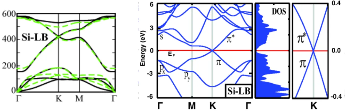
These imaginary frequencies can be interpreted as a dissipation of the energy which causes the instability of the system. The phonon dispersion is shown in figure 1.2(a) [5] in the case of a buckling ∆LB = 0,44 Å, for which optical branches have positive frequencies. At the center of the first Brillouin zone (FBZ) one can observe a linear trend of the acoustical branches. Moreover, the calculations show that the structure is stable in a temperature range quite wide, that is 0 K ≤ T ≤ 1000 K. The most stable structure is found to have a buckling ∆LB = 0,44 Å and a Si-Si distance of 2,25 Å. In figure 1.2(b) [5] the electronic dispersion calculated for LB silicene is presented next to the corresponding density of states (DOS). The most striking feature is the crossing of the π- and π∗-bands at the K and K0 symmetry points of the FBZ, where, moreover, E=EF. This means that silicene
is predicted to have a semi-metallic behaviour, i.e. it is a zero-gap semiconductor. On the very right side of figure 1.2(b) it is shown also a focus on the K-point at the Fermi energy. The evident linear trend implies that electrons near this symmetry point act like massless Dirac Fermions. Fitting the linear trend in the proximity of the K- and K0-point, one estimates the Fermi velocity:
vf ' E(q)/~|q| (1.1)
DFT calculations predict a velocity of ∼ 106 m/s [5], while a tight-binding ap-proach leads to ∼ 105 m/s, that is lower than the one found in graphene (2,5 106 m/s [6]). It has been argued that this is due to the π-bonds, responsible for the conduction inside the sheets, which are weaker in silicene than graphene [4]. Another remarkable consideration pointed out by Cahangirov et al. is that LB
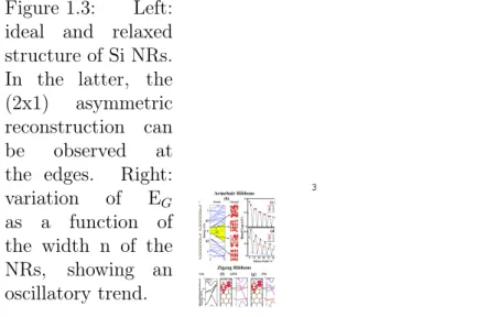
Figure 1.3: Left: ideal and relaxed structure of Si NRs. In the latter, the (2x1) asymmetric reconstruction can be observed at the edges. Right: variation of EG as a function of the width n of the NRs, showing an oscillatory trend. 3 Ban d G ap ( eV )
silicene is ambipolar in the region close to the Fermi level.
Concerning eventual applications, nanoribbons (NRs) of silicene would be of great interest [3]. It is predicted that for n>7, being n the width of the ribbons in terms of number of Si atoms, the structure still shows a LB honeycomb pattern. Considering an armchair arrangement, figure 1.3, the objects appear to be a non-magnetic semiconductor with a non-zero band gap [5]. Of course the quantum confinement effect results in an increase of EG with decreasing values n. Anyway, it can be observed from the plot in figure 1.3 that, just as in graphene, the band
gap shows an oscillatory behaviour as a function of n. The remarkable property of gap engineering can lead to the creation of quantum dots and multiple quantum wells.
Another interesting comparison between graphene and its silicon counterpart is the defects formation. A very common feature one has to deal with when growing ultra-thin films of atoms arranged in honeycomb pattern is the Stone-Wales (SW) defect.
2
TABLE I: Calculated structural and electronic properties for silicene and SW-defected silicene: lattice parameter (a), Si-Si distance (dSi−Si), angle between two of the lattice vectors of a 6×6 supercell (α), total magnetic moment of the system (µT ot), formation energy (Ef), cohesive energy (Ecoh) and the band gap (Egap).
a dSi−Si α µT ot Ef Ecoh Egap ˚
A ˚A deg (µB) (eV ) (eV ) (meV ) Silicene 23.21 2.28 60.0 0 0.00 -3.98 1.5 SW-Silicene 23.04 2.19-2.28 61.5 0 1.64 -3.96 20
for the total energy ground state calculations were cal-culated with the tetrahedron methodology with Bl¨ochl corrections.38
Periodic boundary conditions were employed for sil-icene with a vacuum region of 15 ˚A between neighboring slabs. For supported silicene on a Ag (111) surface the height of the supercell has been set to 29 ˚A in order to conveniently include 4 layers of the Ag crystal. In order to determine the equilibrium configuration of sil-icene with defects, we relaxed all the atomic coordinates and the supercell geometry using the conjugate gradient (CG) algorithm with the maximum residual force of less than 0.01 eV/˚A. The sampling of the Brillouin zone was done for the supercell with the equivalent of 24×24×1 Monkhorst-Pack39 k-point mesh for a silicene unit cell
composed of two Si atoms. In order to minimize the in-teractions between the neighboring SW defects, for the calculation of geometric and electronic properties, we em-ployed a large supercell derived from a 6×6 supercell of silicene where the distance between neighboring defects is at least 14.6 ˚A. The calculations of the formation energet-ics of a SW defect for supported silicene were performed with a 6×6 supercell of silicene on top of 8×8 supercell of Ag (111) surface.
III. RESULTS AND DISCUSSION A. Formation and Stability of Stone-Wales Defects
in Silicene
Since the formation of defects is inevitable in crys-tals, understanding their effect on the mechanical, elec-tronic and structural characteristics plays a key role in nanoscale device applications. The most common defects that have been observed in low-dimensional graphene-like structures are missing atoms, adatom impurities and SW type of disorders. Here we investigate the forma-tion and stability of SW defects in a single layer struc-ture of silicene shown in Fig. 1(a). Compared to the graphitic materials such as graphite, graphene and car-bon nanotubes, the inter-atomic distance is larger in sil-icene. Furthermore, due to the buckled hexagonal lattice structure, easier formation of various defects in silicene can be expected. 0 0.5 1 1.5 2 2.5 3 0° 15° 30° 45° 60° 75° 90° Energ y (eV) a) b) c) 2.31 2.26 116.3° 2.28 117.7° 2.19 120.1° d) 0° 45° 90°
FIG. 1: (Color online) The top and side view of (a) perfect and (b) SW-defected silicene. (c) Energetics of formation of a SW defect in silicene via the bond rotation (highlighted). The black (open squares) curve is obtained by relaxing the first nearest hexagons to the silicene dimer in free-standing silicene layer. Red (open circles) and blue (open triangles) curves are obtained by relaxing up to the second nearest hexagons to the silicon dimer in the free-standing and supported silicene (on a Ag (111) surface), respectively. (d) The actual bond rotation steps (0◦, 45◦and 90◦) in silicene supported on the Ag (111) surface. The uppermost and lower-lying Ag atoms are shown by gray (light) and black (dark).
As shown in Fig. 1(b) a SW defect can be created by the rotation of a silicon dimer by 90◦ around the
cen-ter of the Si-Si bond. From the experimental point of view, such a defect can be formed during the growth process or upon application of irradiation. After the for-mation of the SW defect, four neighboring hexagons of silicene are transformed into a pentagon and a heptagon pair. As can be seen from Fig. 1(b), even after the creation of the SW defect, silicene maintains its buckled two-dimensional structure with only a local out-of-plane displacement of the Si atoms. Conversely, large local bumps in the graphene lattice are formed due to the ex-istence of SW defects. Through 90◦rotation of a dimer,
the Si-Si bond becomes stronger than in defect-free sil-icene and its length decreases from 2.28 to 2.19 ˚A. After the shortening of the bond lengths along the direction parallel to the pentagons, the lattice constant decreases
(a) 4 -1.5 -1 -0.5 0 0.5 1 M K M Energ y (eV) Silicene K M SW silicene a) b) (CB) (CB)K (CB)M (CB) (CB)K(CB)M c)
FIG. 3: (Color online) The electronic band structure for a 6×6 supercell of (a) perfect and (b) SW-defected silicene. (c) Band decomposed charge densities of the conduction band around the Fermi level at Γ, K and M symmetry points (the isosurface is set to 0.57· 10−3e/˚A3)
mation of the SW defect breaks the six-fold symmetry of the silicene lattice, that results in linearly crossing bands and the existence of highly mobile fermions in the vicin-ity of the Dirac point, a band gap opening occurs at the crossing point.40The band gap opening for SW-defected silicene in a 6×6 supercell is calculated to be 0.02 eV. It correspond to the system with a defect concentration of 1.9·1013cm−2. The actual value of the band gap de-pends on the concentration of the SW defects. In the case of a 5×5 supercell with a single SW defect (2.7·1013 cm−2) the energy band gap increases to 0.1 eV. Here it is also worth to note that the choice of a hexagonal super-cell results in band edges that appear at the K symmetry point (Γ for 3n×3n supercells) and a temporarily ordered defect configuration may result in a different band disper-sion. Since there are no dangling bonds introduced into the silicene lattice with the creation of a SW defect, all the atomic orbitals of the Si atoms at the vicinity of the defect are paired and hence there is no defect-originated magnetism.
B. N-doped Silicene: Effect of Stone-Wales Defects
Doping materials with foreign atoms is an efficient way to manipulate their electronic, magnetic and chem-ical properties. For carbon-based materials such as graphite, graphene and nanotubes the doping especially with Group III or V atoms is desirable since they induce n or p type doping and the density of the charge carriers can be tuned by the concentration of the substituents. It has
-1 -0.5 0 0.5 M K M Energ y (eV)
Difference charge density (e -3)
a) b) c) 0.0 0.004 0.011 0.027 0.068 0.170 -0.004 0.003 -0.003
FIG. 4: (Color online) (a) The electronic band structure of N-doped silicene, (b) top and side view of the structure. (c) 3D and contour plot of difference charge density (ρ↑− ρ↓).
The slicing plane is marked by dot-dashed line in (b).
been demonstrated that synthesis of N doped graphene samples can be achieved by annealing in the presence of pyridine or NH3 molecules and by chemical vapor de-position (CVD) and the observed features of N-doped graphene are quite desirable for device applications.41–45 The formation energy of N substitution in graphene is 0.32 eV per N atom.46Since N atom in graphene forms three σ bonds and pzorbital is filled by two electrons, N-doped graphene shows nonmagnetic behavior.41The N doping induces n-type doping of graphene and shifts the Fermi level up by∼ 0.6 eV for the case of 2 % N concentration.42
The substitutional doping of silicene with a N atom is of a different nature as compared to the doping of graphene. The N-Si bond length in substituted silicene (1.83 ˚A) is significantly shorter than the Si-Si bond length in pristine silicene (2.28 ˚A) and the shorter bonds induce a local in plane shrink deformation in the structure as presented in Fig. 4(b). The nitrogen bonds with the neighboring Si atoms are in the plane, which reduces the amount of local buckling. However, perfect silicene’s lat-tice structure is restored just several bonds away from the substituent atom. The formation energy of N-doping in silicene is defined as
Ef= ET ot− (ESilicene− µSi)− µN (3) where Etotis the total energy of the N-doped silicene and ESiliceneis the total energy of perfect silicene, µSi is the chemical potential of a single silicon atom (calcu-lated from the total energy of monolayer silicene), and
(b)
Figure 1.4: (a) structure of free standing silicene and relative calculated equi-librium distances, in the absence (left) and presence (right) of SW defects. (b) Dispersion curves associated to the structures in (a), top left and top right respec-tively. On the bottom are plotted the charge densities of the conduction band near the Fermi energy at high symmetry points of the FBZ. [9]
This defect consists in the 90° rotation of two bounded atoms of the layer, which results in the formation of two heptagons and two pentagons surrounding the rotated couple, figure 1.4(a). The potential barrier for the formation of defects is substantially smaller in silicene compared to graphene, ∼2,4 eV and ∼9,2 eV respectively. Moreover, the inverse process, that is the relaxation of the defects, still shows a potential barrier of ∼0,76 eV, which guarantees the stability of such defects also at modest temperatures [9]. The dispersion curves for ideal and SW silicene are plotted in figure 1.4(b). The K and K0 symmetry points are folded onto the Γ point. The most interesting effect of the presence of defects in the layer is that a gap is opened in the vicinity of the Dirac point. Its value depends on the concentration of defects; for example, considering a 6x6 supercell with a defect concentration of 1,9 1013 cm−2 the gap is calculated to be 0,02 eV. These considerations can be pushed more forward speculating about the possibility of doping in the presence of defects. In particular Sahin et al. [9] prove that the doping of silicene with N atoms transform the classical semi-metallic material into a ferromagnetic metal with total magnetization 1,0 µB.
More properties, even more exotic than the ones cited, have been predicted and are still investigated, but their description lies outside the general purpose of this work.
1.3
Experimental observations of silicene
The first claim of an experimental observation of silicene dates back to 2010. The first studies dealt mainly with silicon deposition on Ag(110) and Ag(111), for which a description will be given. Nevertheless, it is worth noting that the electronic properties showed by silicon deposited on metal surfaces are altered by strong silicon-metal interaction, which makes questionable the silicene nature of the structures studied. In particular in this section and in the next chapter, the possibility of a misleading interpretation of some results obtained in the last years will be discussed, concerning the presumed observation of epitaxially grown silicene sheets on Ag(111) and MoS2 [10,25] and silicene NRs on Ag(110) [11].
1.4
Silicene nanoribbons (NRs) on clean Ag(110)
It has been observed that the deposition of silicon onto a clean Ag(100) results in the formation of one dimensional silicene structures, i.e. nanoribbons, well aligned along the (-110) direction and with a characteristic width of 16 Å [11,12]. It has been reported that changing the substrate temperature, NRs form with different widths, i.e. 0,8 and 1,6 nm figure 1.5 [14].
RAPID COMMUNICATIONS
ROMAIN BERNARDet al. PHYSICAL REVIEW B88, 121411(R) (2013)
FIG. 1. (Color online) (a)–(d) Sequence of STM images (234 × 234 nm2) of the same area showing the evolution of the Ag(110) surface
upon Si deposition at RT. I = 510 pA, Vsample = 1.5 V. (a) Bare silver surface. Colors correspond to the different terraces separated by
monoatomic Ag steps. The upper terrace is at the right side of the image (red). (b) θSi = 0.1 ML. (c) θSi = 0.2 ML. (d) θSi = 0.3 ML.
(e) evolution of the density of Ag atoms incorporated as a function of the Si coverage. (f) STM image recorded at TLN2of nanoribbons grown
on Ag(110) upon Si deposition at RT. θSi∼ 0.3 ML. I = 300 pA, Vsample= 1 V.
same width of 2ax (∼0.8 nm) and the same apparent height.
Few of the observed NRs present a width of 4ax (∼1.6 nm),
corresponding to four rows of protrusions. We emphasize that these NRs differ only in width from the single ones and will be denoted hereafter double NRs (DNRs).
Figures1(a)–1(d)show a series of four large scale STM
im-ages of the bare surface and the same surface area immediately after three successive Si depositions performed in the same
conditions at RT. Figure1(a)corresponds to the bare Ag(110)
surface and shows flat terraces separated by monoatomic steps. Some portions of steps, close to the [1¯10] direction, are straight while others, pinned by defects or impurities, are misoriented from this dense direction. Steps appear slightly frizzy due to adatoms moving along the step edges. After the first Si
evaporation corresponding to θSi= 0.1 ML, a clear motion of
the step edges is visible in Fig.1(b), leading to an increase
of their meandering. Isolated NRs, parallel to the straight parts of steps can also be distinguished. After the second Si deposition, the deformation of steps is more pronounced [see
Fig. 1(c)]. Misoriented parts of step edges appear serrated
with the formation of fingers. Upon further Si evaporation, these fingers continue to grow and additional elongated shape islands form on the terraces [see Fig.1(d)].
The detailed view in Figs.2(a)and2(b)provides valuable
information on the features observed. These STM images have been recorded after the second and the third Si depositions
FIG. 2. (Color online) (a),(b) STM images (75 × 82 nm2)
show-ing the growth of fshow-ingers from steps perpendicular to the NRs upon Si deposition at RT. I = 510 pA, Vsample= 1.5 V. (a) θSi= 0.2 ML.
(b) θSi= 0.3 ML. (c) and (d) Height profiles along the white transverse
lines in (a) and (b), respectively.
121411-2
Figure 1.5: Single nanoribbons (SNR) of ∼0,8 nm, and double nanoribbons (DNR) of 1,6 nm of width. ax and ay are the basis vector of the Ag surface.
It has been reported [12] that performing evaporation with a substrate temperature of 230 °C a better structural ordering can be obtained. In figure 1.6(a) filled-states STM image is presented next to the model for its description. The shortest distance between protrusions is 0,335 nm, much larger than the expected 0,235 nm for bulk silicon [3] or 0,225 nm for silicene [5], from which it can be argued that it doesn’t represent the Si-Si distance. Assigning this protrusions to the second neighbour atoms, the more realistic silicon distance of 0,193 nm is obtained, figure 1.6(b). Thus, assuming that not all the atoms are resolved in the STM images, a realistic model is obtained. Nevertheless, two recent works [14,15] undermine the hypothesis of the silicene nature of the NRs mentioned above, when they cover completely the silver substrate. Bernard et al. have observed, by means of grazing incident X-ray diffraction (GIXD) and STM studies, that the silicon deposition induces a reconstruction of the Ag substrate, despite the non-miscibility of the two-elements. Moreover, Borensztein et al. exploit surface differential reflectance spectroscopy to observe important differences between the absorption predicted for
the 0.193 nm value measured in this study and previously [15, 29].
Figure 3. a) Atomically resolved filled-states STM image of silicene NRs grown at 230 C
on a Ag(110) surface (6x6 nm2, V = -0.2 V, I = 1.9 nA). b) Proposed model where the grey
and yellow atoms correspond to the first and the second silver layers, respectively. The blue honeycomb structure corresponds to the internal structure of silicene NRs while the red one corresponds to the structure observed in the STM image.
The second explanation is an electronic contribution to the periodic structure in the STM images, which is controlled by the interaction between the atoms of the silicene and the rows of underlying Ag atoms. The graphene and silicene honeycomb structure has a Bravais lattice containing two atoms which leads to an inequivalence between the sub-lattices ”a” and ”b”. Inspection of Figure 3a immediately shows that the red hexagons occupy 2/3 of the atoms of one lattice and the central ”chains” are aligned between the Ag atom rows. Recently, theoretical calculations indicate that electron transport occurs coherently via atoms of the same sub-lattice [31]. Also, the 1D nanoribbon confines the 2D electron gas giving rise to electron scattering at armchair edges with the formation of quantum interferences localized on the bonds [25]. These two related e↵ects indicate that the electron density is channeled along the nanoribbons. 4. Conclusion
In conclusion, we have presented a detailed experimental study of the epitaxial growth of silicon on Ag(110), held at 230 C. The STM images reveal a self-assembled compact array of silicene nanoribbons with a very low density of defects. The NRs are tens of nanometers in length with a uniform width of 1.6 nm, and commensurate with the Ag(110) surface giving a (2x5) periodicity in the LEED measurements at saturation (1ML). We propose an atomic model of silicene nanoribbon with arm-chair edges. Careful scrutiny of the atomically resolved STM images, taken at several imaging conditions, indicates that not all silicon atoms in the NRs are observed. This is explained by a substantial buckling of the NRs and an electronic contribution due to the quantum confinement of the electrons in the NRs.
d
Figure 1.6: (a) Filled-state image of silicene NRs grown at 230 °C on Ag(110) (6x6 nm2, V=-0,2 V, I=1.9 nA). (b) Proposed model to interpret the STM images of Si NRs: the red honeycomb net represents the Si atoms evident in the acquired images; the blue net represents the actual configuration of the silicon atoms. It seems reasonable to think that the non-resolved atoms are the buckled ones in the NRs structure.
silicene and the one observed for the NRs. Thus, these two last observations make highly questionable the silicene nature of the nanoribbons, as silver contribution in the assembling process cannot be excluded.
1.5
Silicene growth on Ag(111)
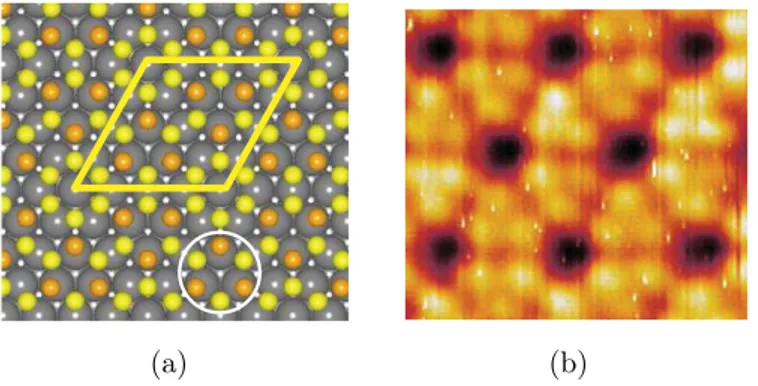
Given the hexagonal close packed arrangement of its atoms and its smooth surface potential [3], the (111) face of the transition metals appears to be ideal for the growth of 2D thin films and sheets. It appears particularly suited for Si deposition, as the two materials are almost non-miscible [16]. Silicon grown on Ag(111) bare substrates has been studied exploiting atomic resolved scanning tunnelling microscopy and LEED [17]. The images obtained show that a rotated honeycomb arrangement of atoms appears on the sample after silicon evaporation, figure 1.8(b). A LEED analysis, figure not shown by Lalmi et al. [17], confirms that this pattern is associated to a (2√3 x 2√3)R30° superstructure, leading to
the model shown in figure 1.8(c). It is worth noting that the Si-Si distance found in this study is 0,19 nm, that is 17% shorter than the one in bulk silicon (0,235 nm) [17].
of 0.22 nm (! 0:01 nm), in excellent agreement with the theoretical predictions for silicene [9].
In order to clarify the energetic stability of the suggested structure model, ab initio calculations based on DFT were performed, including full structural relaxations. These cal-culations reveal that the total energy for the structure model shown in Fig. 4(c) has a negative value and an adhesion energy of "0:48 eV for each Si atom, demon-strating that the silicene arrangement on Ag(111) is ener-getically stable. The obtained relaxed geometry is depicted in Fig.5(a) (top view) and Fig.5(b) (side view). It can be seen that the Si atoms of the silicene layer which are located directly on top of underlying Ag atoms are slightly displaced in z direction with respect to the bottom Si atoms. The distance between the top (bottom) Si atoms and the average height of the first Ag layer is 0:292! 0:002 nm and 0:217! 0:003 nm, respectively. As a result of this displacement, triangular structures are formed in the silicene top layer consisting of three Si atoms, which are separated by 0.38 nm. This is in very good agreement with the experimental STM observations that show the same triangular structure and a separation of approximately 0.40 nm. In Fig. 5(c), a hexagonal silicene ring from (a) [indicated by the white circle in (a)] is shown in top and side view. The theoretically determined Si-Si distance is 0.232 nm, which also agrees very well with the experimen-tally determined value of 0.22 nm, and top and bottom Si atoms are separated by 0.075 nm. Following these
calculations, we have also determined the bond angles of the Si atoms, which also give information on the hybrid-ization state of the respective atom. In detail, we find, for the six top Si atoms of the (4# 4) unit cell, bond angles of $ 110% (!), which is very close to an angle of 109.5% for
an ideally sp3-hybridized Si atom. From the remaining 12 bottom Si atoms, six are purely sp2hybridized (bond angle
of $ 120%) and six have bond angles of between $ 112% and$ 118%("), indicating a sp3=sp2hybridization. These
different bond angles of the Si atoms result from the displacement of the Si atoms in z direction caused by the interaction with the Ag(111) substrate. However, most of the atoms are sp3=sp2 hybridized, which is probably the
equilibrium state, in agreement with calculations for free-standing Si [9].
Based on the relaxed geometry, STM images were simulated by calculating the local electron density of states according to the Tersoff-Hamann approach [24]. In Fig. 5(d), it can be seen that the simulated STM image exhibits the same structural features as those observed experimentally, i.e., a hexagonal arrangement of the trian-gular structure around dark centers. By looking at the charge density around top and bottom Si atoms (not shown here), we find that they are electronically very similar. That means that the STM corrugation is mainly dominated by geometrical aspects rather than by electronic effect, which
FIG. 4 (color). Construction of the atomic structure model for
the 2D Si adlayer. Filled-states STM images of (a) the initial
clean Agð111Þ-ð1 # 1Þ surface (Ubias ¼ "0:2 V, I ¼ 1:93 nA)
and (b) the (4# 4) silicene sheet (Ubias ¼ "1:4 V, I ¼
0:29 nA). (c) Model of silicene on Ag(111). Si atoms sitting on top of Ag atoms are highlighted as larger orange balls, resembling the measured STM image. In the bottom right corner, the ball-and-stick model for the freestanding silicene layer is shown with an Si-Si distance of 0.22 nm.
(a)
(d)
(c)
(b)
FIG. 5 (color). DFT results for the silicene on Ag(111). (a) Top
view of the fully relaxed atomic geometries of the model for
silicene on the Ag(111) surface from Fig.3. (b) Side view of (a).
c) Enlarged image of the hexagonal silicene ring indicated by the white circle in (a). (d) Simulated STM image (left) for the structure shown in (a). The simulated image exhibits the same structural features as those observed in the experimental STM image (right), i.e., a hexagonal arrangement of the triangular structure around dark centers.
PRL 108, 155501 (2012) P H Y S I C A L R E V I E W L E T T E R S 13 APRIL 2012week ending
155501-4
(a)
of 0.22 nm (
! 0:01 nm), in excellent agreement with the
theoretical predictions for silicene [
9
].
In order to clarify the energetic stability of the suggested
structure model, ab initio calculations based on DFT were
performed, including full structural relaxations. These
cal-culations reveal that the total energy for the structure
model shown in Fig.
4(c)
has a negative value and an
adhesion energy of
"0:48 eV for each Si atom,
demon-strating that the silicene arrangement on Ag(111) is
ener-getically stable. The obtained relaxed geometry is depicted
in Fig.
5(a)
(top view) and Fig.
5(b)
(side view). It can be
seen that the Si atoms of the silicene layer which are
located directly on top of underlying Ag atoms are slightly
displaced in z direction with respect to the bottom Si
atoms. The distance between the top (bottom) Si atoms
and the average height of the first Ag layer is 0:292
!
0:002 nm and 0:217
! 0:003 nm, respectively. As a result
of this displacement, triangular structures are formed in the
silicene top layer consisting of three Si atoms, which are
separated by 0.38 nm. This is in very good agreement with
the experimental STM observations that show the same
triangular structure and a separation of approximately
0.40 nm. In Fig.
5(c)
, a hexagonal silicene ring from (a)
[indicated by the white circle in (a)] is shown in top and
side view. The theoretically determined Si-Si distance is
0.232 nm, which also agrees very well with the
experimen-tally determined value of 0.22 nm, and top and bottom
Si atoms are separated by 0.075 nm. Following these
calculations, we have also determined the bond angles of
the Si atoms, which also give information on the
hybrid-ization state of the respective atom. In detail, we find, for
the six top Si atoms of the (4
# 4) unit cell, bond angles of
$ 110
%(!), which is very close to an angle of 109.5
%for
an ideally sp
3-hybridized Si atom. From the remaining 12
bottom Si atoms, six are purely sp
2hybridized (bond angle
of
$ 120
%) and six have bond angles of between
$ 112
%and
$ 118
%("), indicating a sp
3=sp
2hybridization. These
different bond angles of the Si atoms result from the
displacement of the Si atoms in z direction caused by the
interaction with the Ag(111) substrate. However, most of
the atoms are sp
3=sp
2hybridized, which is probably the
equilibrium state, in agreement with calculations for
free-standing Si [
9
].
Based on the relaxed geometry, STM images were
simulated by calculating the local electron density of
states according to the Tersoff-Hamann approach [
24
]. In
Fig.
5(d)
, it can be seen that the simulated STM image
exhibits the same structural features as those observed
experimentally, i.e., a hexagonal arrangement of the
trian-gular structure around dark centers. By looking at the
charge density around top and bottom Si atoms (not shown
here), we find that they are electronically very similar. That
means that the STM corrugation is mainly dominated by
geometrical aspects rather than by electronic effect, which
FIG. 4 (color). Construction of the atomic structure model for
the 2D Si adlayer. Filled-states STM images of (a) the initial
clean Agð111Þ-ð1 # 1Þ surface (Ubias¼ "0:2 V, I ¼ 1:93 nA)
and (b) the (4# 4) silicene sheet (Ubias¼ "1:4 V, I ¼
0:29 nA). (c) Model of silicene on Ag(111). Si atoms sitting on top of Ag atoms are highlighted as larger orange balls, resembling the measured STM image. In the bottom right corner, the ball-and-stick model for the freestanding silicene layer is shown with an Si-Si distance of 0.22 nm.
(a)
(d)
(c)
(b)
FIG. 5 (color). DFT results for the silicene on Ag(111). (a) Top
view of the fully relaxed atomic geometries of the model for
silicene on the Ag(111) surface from Fig.3. (b) Side view of (a).
c) Enlarged image of the hexagonal silicene ring indicated by the white circle in (a). (d) Simulated STM image (left) for the structure shown in (a). The simulated image exhibits the same structural features as those observed in the experimental STM image (right), i.e., a hexagonal arrangement of the triangular structure around dark centers.
PRL 108, 155501 (2012)
P H Y S I C A L
R E V I E W
L E T T E R S
13 APRIL 2012week ending155501-4
(b)
Figure 1.7: (a) Ideal organisation of silicon atoms on Ag(111) in a 4x4 superstruc-ture and corresponding STM image reported (b).
These results, of course, are far from being conclusive regarding the silicene na-ture of the 2D arrangement observed. In order to prove or disprove this hypothesis, Vogt et al. [19] presented a combined STM and angular-resolved photoemission spectroscopy (ARPES) work, claiming to have observed a linear dispersion at the K-point of the FBZ, after having evaporated silicon on an Ag(111) substrate, from which a Fermi velocity of 1,3 · 10−6 m/s was deduce, which is even higher than the one reported for graphene. The superstructure observed this time with STM, and confirmed by LEED, showed a 4x4 supercell, figure 1.9(a). Nevertheless, the expected sp band of the bare Ag(111) is not shown and further studies assigned the linear dispersion to the folding of such a band into the FBZ and confirmed that the Dirac cone in the 4x4 silicene phase is destroyed as a consequence of strong Si-Ag interaction [3].
Following the first observation of an epitaxial layer grown on Ag(111), more experiments have been performed, focusing the attention on the role of the tem-perature of the substrate. It has been observed [20] that employing temtem-peratures above 330 °C no superstructure was observed. On the contrary, at temperatures below this one, an evolution from the (4x4) surface pattern, at T=150 °C, to the (2√3 x 2√3)R30°, at T=300 °C, was noted. In the range between these temper-atures, both phases are present, plus a (√13 x √13)R13,9°. These considerations
9
Figure 3
Figure 1.8: Filled-state images of the bare Ag(111) substrate (a) and of (2√3 x 2√3)R30° superstructure observed after the evaporation of silicon. In (c) it is made more clear 2√3ratio between the new lattice vectors (red arrows) and the ones of the hcp silver structure. The rotation between the two honeycomb arrangement is highlighted, too.
are deduced by means of LEED, figure 1.9, and STM measurements performed after the deposition of about 1 ML of silicon.
Concerning the role of the coverage into the reconstructions, it has been ob-served [21] that maintaining the substrate in the temperature range 200-220 °C, the first layer deposited shows a 4x4 superstructure. Increasing the coverage, a (√3x√3) pattern appears to be more and more important until it finally becomes dominant after ∼5 MLs deposition. Note that this reconstruction has been never observed for silicon. Just relying on the step height observed for the (√3 x √3), the superstructure has been interpreted as a silicene monolayer.
Anyway, a recent STM study showed also that the growth of silicene-like sheets on Ag(111) comes along with the release of about 65% of the silver atoms from the Si covered areas [24], showing that the two materials do interact, despite
J. Phys.: Condens. Matter24 (2012) 172001 Fast Track Communication
Figure 1. LEED diagrams obtained after the deposition of about one silicon monolayer on Ag(111) maintained at different temperatures: (a) a quasi-pure (4 ⇥ 4) at 150 C; a mixture of (4 ⇥ 4), (p13 ⇥p13)R13.9 and (2p3 ⇥ 2p3)R30 superstructures, respectively, at (b) 210 C and (c) 270 C, and (d) a quasi-pure (2p3 ⇥ 2p3)R30 at 300 C.
Figure 2. (a) Filled-states atomically resolved STM image after deposition of one silicon monolayer at 150 C showing a (4 ⇥ 4) superstructure (I = 1.0 nA, U = 1.4 V). Inserted in the right corner is a filled-states atomically resolved STM image of the clean Ag(111) surface at the same scale and recorded before the silicon deposition. (b) Line profile showing the distance between two black neighboring holes giving the periodicity.
3.3. Ball models of the three superstructures
From STM images, which only reflect a map of the surface density of states, it is generally difficult to deduce an atomic model. Nevertheless, the observation of regular hexagons on these superstructures on the one hand and the previous results obtained on the Ag(110) face showing silicene nanoribbons on the other hand, let us assume that the same structure
can exist on silver (111), i.e. a silicene layer with a honeycomb structure grown on top of the Ag(111) surface. This assumption is strongly supported by the intrinsic perfect match between four nearest-neighbor Ag distances (1.156 nm) and three unit cells of the (111) surface of silicon (1.152 nm) forming a natural (4 ⇥ 4) superstructure (see the model of figure6(a)) [17]. In the unit cell of this ball model, many silicon atoms are situated in threefold sites or in bridge 3
Figure 1.9: LEED images acquired after the deposition of ∼1 ML of silicon on a Ag(111) substrate at different temperatures. (a) 4x4 superstructure, T=150 °C. (b)-(c) spots originating from (4x4), (2√3 x 2√3)R30° and (√13 x √13)R13,9°, respectively at 210 °C and 270 °C. (d) (2√3x 2√3)R30° superstructure.
their immiscibility. In particular large scale STM images show that at the very beginning of Si evaporation at T=167 °C, step edges undergo stabilization and faceting along the h110i direction figure 1.10(a). This is caused by the diffusion of silicon atoms which interact with Ag at the step edges, modifying their shape. Further evaporation causes the nucleation of islands on the terraces and strips at the step edges. At higher coverages, dentritic features develop, which appear very smooth with no atomically resolved structure, figure 1.10(e). The height of these features is 0,236 nm that is exactly the height of a single Ag(111) step, figure 1.10(f). Thus, these features clearly involve silver.
Concerning multi-layers silicene structures, it has been recently argued [22] that long silicon evaporation on a Ag(111) substrate results in the formation of a thin film of bulk-like silicon terminated with the Si(111) √3 x √3-Ag surface. LEED analysis shows that after the first monolayer deposition a 4x4 superstructure is
Figure 1.10: Si evaporation on Ag(111) at T=167. (a) clean silver surface. (b) Very beginning of the evaporation: note the faceting of the step edges along the h110i direction. Coverage: 0,09 MLs. (c)-(e) Increasing Si deposition: 0,28; 0,49; 0,74 respec-tively. (f) Profiles relative to the black line in (a) and the red one in (e).
Thus, when one region was being scanned, the other one was fully exposed to the Si beam, which allowed us to follow the evolution of both regions during the growth process. Surface morphologies obtained in this way were identical to those observed on regions far from the shadow of the tip for simi-lar coverages.
The evolution of one region during Si deposition at Tsample¼ 167"C is shown in Figure1(see also the movie27).
STM images are drift-corrected and extracted from larger images using the surface defects as reference points in order to show the evolution of a very precise and well defined area. Prior to evaporation (Figure1(a)), the Ag(111) surface displays large flat terraces which are represented by different colours as a function of their vertical position. Successive images of the same region before the deposition did not show any significant difference, demonstrating the low mo-bility of the step edges and the stamo-bility of the surface before the deposition. Despite the high mobility of Ag adatoms on the (111) surface, step fluctuations are reduced due to the pinning of their edges at surface defects, leading to curved shapes.28At the very beginning of evaporation (Figure1(b)),
stabilization and faceting of step edges towards theh110i orientations occurs. This indicates that Si atoms diffuse on the Ag(111) terraces and strongly interact with Ag atoms at a step edge, resulting in a change of its equilibrium shape. A detailed image of such step edge (Inset of Figure1(b)) shows a periodicity equal to twice the Ag-Ag distance (0.578 nm). This is in agreement with STM studies after Si deposition on Ag(110), which showed faceting of the (110) surface into a (211) surface composed by small (111) terraces, with the same#2 periodicity along the [1!10] step edges separating the terraces.25DFT calculations suggest that Si atoms
par-tially substitute Ag atoms in the step edges.25Faceting of
steps on Ag(111) is therefore a first hint of the strong Si-Ag interaction. In Figure1(b), the formation of islands on terra-ces and of strips along step edges is also visible. They dis-play a very similar rough aspect on STM images and both appear at a lower apparent height than the surrounding ter-race. They result from the nucleation of Si on the terraces or at the step edges. However, as there is no direct relationship between the actual topography of a surface and the STM ob-servation, which probes the electron density of the surface, we cannot determine the relative position of the Si atoms with respect to the Ag surface plane. The region in the vicin-ity of a step on the upper terrace remains free of Si-islands, which is not the case on the lower terrace. It suggests that the nucleation of strips at step edges is mainly due to Si atoms diffusing from the upper terraces. Similar observations are made for growth at 205"C (see Figure S1 (Ref.27)). At this higher temperature, the Si-island density at the end of the nucleation phase is lower ($4 # 10%5nm%2instead of
$10%4nm%2) and the ratio between the areas covered by
Si-strips and Si-islands is higher.
Figures1(c)–1(e)show the further growth of these struc-tures during the deposition. Strips thicken nearly homogene-ously while islands adopt a triangular shape with edges along theh110i directions, especially at 205"C (see Figure S1 (Ref.27)). We have also followed their evolution at a lower scale. For small sizes, they do not show any long range atomic ordering. For sizes larger than 30–50 nm, ordered structures begin to form. A detailed view of a Si-strip grow-ing at 205"C is presented in Figure2for two coverages (0.6 ML and 0.8 ML). Although the resolution is poorer for Figure2(a)than for Figure2(b), one can distinguish between different structured domains and observe their evolution with increasing Si amount. In order to better visualize the reconstructions, the different domains have been colored, whereas disordered domains and the bare Ag substrate are shown in grey. From the angle and distance measurements, domains ofð4 # 4Þ (pink) and ðpffiffiffiffiffi13#pffiffiffiffiffi13Þ R13.9"(blue) are identified. In addition, a structure formed by apparent dots appears with a period around 1.006 0.02 nm, in agree-ment with possibleð2pffiffiffi3# 2pffiffiffi3Þ R30"and (3.5# 3.5) R26" reconstructions previously proposed (yellow). However, no specific orientation with respect to the substrate is clearly found for this latter structure. Comparison between Figures
2(a)and2(b)shows that the Si strip undergoes several modi-fications upon growth.ð4 # 4Þ and ðpffiffiffiffiffi13#pffiffiffiffiffi13Þ domains grow at the expense of disordered regions. The dotted struc-ture is also not stable. Such strucstruc-ture has been previously assumed to be a precursor of theð4 # 4Þ structure.8Here, we
FIG. 1. Evolution, during Si evaporation at 167"C, of the same region of the
Ag(111) surface. (a) Bare surface. (b)–(e) For Si coverages of 0.09, 0.28, 0.49, and 0.74 ML, respectively. Size of the images: 325# 325 nm2
. Tunneling conditions: 1.5 V, 30 pA. The inset in (b) (4.3# 4.3 nm2
) is a detail of a step edge on another part of the surface at the very beginning of Si evaporation. (f) Profiles for bare surface (black) and 0.74 ML (red) along the same line drawn in (a) and (e). The Ag step height is 0.236 nm.
213106-2 Pr"evot et al. Appl. Phys. Lett. 105, 213106 (2014)
This article is copyrighted as indicated in the article. Reuse of AIP content is subject to the terms at: http://scitation.aip.org/termsconditions. Downloaded to IP: 134.157.36.20 On: Mon, 08 Jun 2015 16:47:16
present at the surface. Afterwards, for longer Si evaporation, the (√3x √3) spots emerge in the images, in agreement with the previous work. At this point, LEED I-V curves were acquired and compared to the ones calculated for silicene layers, highlighting important differences between them. Thus, it was noted that these IV curves resemble the same kind of curves obtained for Si(111) √3x√3-Ag surface. Calculated and experimental result gave this time a good agreement.
As the Ag(111) substrate was made from the deposition of silver onto Si(111), in order to be sure that during the process of annealing no break in the Ag(111) occurred causing the Si(111)√3x√3-Ag surface to form, further verifications have been made, excluding this eventuality. Thus, it was concluded that Ag acts as a surfactant in the Si growth process, meaning that silver atoms remain segregated at the surface.
These considerations will be useful in the third chapter when LEED, AES and SDRS results after long silicon evaporation on Ag(111) will be presented.
RAPID COMMUNICATIONS
TERUFUSA SHIRAI et al. PHYSICAL REVIEW B 89, 241403(R) (2014)
) b ( ) a ( ) d ( ) c ( (e) Ag 1× 1 Si 1× 1 Silicene 3× 3 Single-Layer Silicene (f) Silicene 3× 3 Multi-Layer Silicene V e 2 8 V e k 5 1 a* b*
FIG. 1. (Color online) RHEED and LEED patterns for Ag(111)-1 × Ag(111)-1 [(a) and (b)], single-layer silicene (3 × 3) [(c) and (d)], and
multilayer (∼4 MLSi) silicene (√3 ×√3) [(e) and (f)], respectively.
The RHEED (LEED) patterns were taken at room temperature (100 K). The incident electron energy is 15 keV, and 82 eV, respectively.
throughout this Rapid Communication. The LEED patterns
shown in Fig.
1
were taken at 82 eV. After Si deposition at
500 K, additional spots appear, as shown in Figs.
1(c)
and
1(d)
. Red arrows or circles correspond to spots for the Si
1 × 1 periodicity. The yellow circles in the LEED pattern of
Fig.
1(d)
correspond to the 3 × 3 (or 4 × 4 in terms of the Ag
lattice) spots that have been identified as the signature of the
completion of the first Si layer on Ag(111) [
7
,
18
]. However
in the RHEED pattern of Fig.
1(c)
, there is no clear 3 × 3
periodicity, and only some additional spots at the zeroth Laue
zone (yellow arrows) appear. This may be due to the fact
that the sample was cooled down in the LEED measurements
to 100 K, while the RHEED observation was done at room
temperature (Debye-Waller effect). Since the yellow arrow
spots were observed every time the silicene sample was
fabricated, we regard this as the signature of the completion of
the single-layer silicene on Ag(111). After further deposition
of Si, namely, about twice the amount of deposition time
as that shown in Figs.
1(c)
and
1(d)
, clear
√
3 ×
√
3 spots
appear as can be seen in Figs.
1(e)
and
1(f)
(green arrows and
circles). Even the first Laue zone of the Si(111) periodicity
can be observed in Fig.
1(e)
(short green arrows), and the
1 × 1 spots of the Ag(111) lattice become weak (orange
arrows and circles). This is consistent with previous reports
and can be regarded as the formation of multilayer silicene
[
10
,
18
]. We have also found that the
√
3 ×
√
3 is preserved
even when Si is further deposited and the Si thickness for the
sample shown in Figs.
1(e)
and
1(f)
is 4 ML
Si. We will call it
“M-silicene” hereafter.
The red curves in Figs.
2(a)
and
2(b)
show the
experimen-tally determined LEED I V curves for the M-silicene sample
shown in Figs.
1(e)
and
1(f)
. Eight different spots in the LEED
pattern have been plotted. Despite the threefold symmetry of
the
√
3 ×
√
3 structure, the symmetrically inequivalent spots,
such as (1 0) and (0 1) spots, exhibited almost the same
I V
curves. This is because there are twin domains on the
surface, which are mirror reflected to each other, and thus their
superposition leads to the apparent twofold symmetry. Taking
this double-domain surface into account, we took the average
of the I V curves both in the calculation and in the experimental
data such that {hk} is the average of the two double-domain
symmetric points (hk) and (kh). Note that some spots such as
(2/3 2/3) do not need averaging. The details concerning the
symmetry will be discussed further later in Fig.
3
.
Now let us move on to the analysis of the experimental
data. As a starting point for the analysis, we have adopted
structure models that have been proposed in the literature
[
12
,
23
,
24
]. They are basically multilayer buckled silicene
structures stacked in different sequences [
12
]. The substrate Ag
atoms are considered in some models [
23
,
24
]. We have
varied the amount of buckling (0.05–0.8 ˚A) and the interlayer
distances between the layers (1.0–3.0 ˚A) considering the
height difference reported in STM studies [
9
,
15
]. Four topmost
buckled Si layers were allowed to relax. However, we were not
able to reproduce the experimental data for any of the proposed
models (R
pwas 0.6–0.8).
Therefore, we reached the conclusion that it is likely that the
M-silicene we experimentally fabricated is not only composed
of Si. In fact, we realized that the experimental curves of
Figs.
2(a)
and
2(b)
are similar to those of the Si(111)
√
3 ×
√
3-Ag surface reported in Refs. [
28
] and [
29
]. Hence we have
adopted the honeycomb-chain triangle (HCT) [Fig.
2(c)
] [
30
]
and inequivalent triangle (IET) models [Fig.
2(d)
] [
31
] as
the initial structure and performed the LEED I V analysis
[
32
]. The topmost Ag layer as well as the four Si bilayers
below were allowed to relax and below it, the parameters
for the diamondlike Si(111) bilayers (buckling = 0.78 ˚A
and interlayer distance = 2.35 ˚A) were used [Fig.
2(e)
]
[
33
]. The comparison between experiment and calculation is
shown in Figs.
2(a)
and
2(b)
, which show nice agreement
[R
p= 0.22 ± 0.03 in (a) and R
p= 0.19 ± 0.03 in (b)]. The
optimized structure is shown in Fig.
2(e)
, and we can say that
the structure is close to a diamondlike silicon terminated with
√
3 ×
√
3-Ag structure at the surface. The Debye temperature
and other parameters are also shown in Fig.
2(e)
, and they are
close to those reported in Refs. [
28
–
30
].
Our analysis above suggests that M-silicene is basically
a diamond-lattice silicon film with Si(111)
√
3 ×
√
3-Ag at
the surface. However one needs to be careful before reaching
241403-2
Figure 1.11: LEED im-age acquired after the deposition of ∼4 MLs of silicon on a Ag(111) substrate. The spots relative to bulk-like sil-icon are highlighted in red, while in green it has been highlighted the spots of the √3 x √3 superstructure. The or-ange circle is associated to the bare silver sub-strate.
1.6
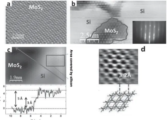
2D Silicon nanosheets on MoS
2So far it has been showed that the interaction between silver and silicon ham-pers the silicene nature of the 1D and 2D structures observed after Si evaporation on Ag(110) and Ag(111). Obviously, it is desirable to find a substrate which could provide a template for the growth of silicene, avoiding as much as possible their mutual interaction, so that the Si-induced features could realistically show a silicene nature, not only in the structure, but also in the properties.
Figure 1.12: MoS2 sandwich stack structure. 15
Layered graphite-like materials with hexagonal crystal symmetry appear to be promising candidates for such a task, being non-metallic substrates quite suitable for the 2D growth of silicon with an honeycomb arrangement. The cleavage of such layered compounds does not create dangling bonds, making them ideal inert surfaces for van der Waals epitaxy of weakly interacting silicon films [25]. For ex-ample, MoS2comprises a stack of S-Mo-S sandwiches and the basal surface consists of a chemically-inert layer of sulphur atoms [40]. The absence of orbitals suitable for bondings between the MoS2 sandwiches accounts for the lack of reactivity of the material. Each molybdenum atom is bonded to three sulphur atoms above and below, figure 1.12.
Figure 1.13: (a) Clean MoS2. (b) Partially covered MoS2after 0,8 ML Si deposition and relative RHEED pattern (inset). (c) Image acquired with different parameters (higher bias, lower set current) of a partially covered surface. In the inset is presented the profile taken along the arrow in the STM image. (d) Atomically resolved image acquired onto a silicon covered area and proposed model, in which the honeycomb silicon lattice is superimposed to the one of the substrate.