1
Abstract— In this work, the implication of the incremental
pulse and verify (IPV) algorithm onto the Forming, Set and Reset read current distributions is studied in terms of inter-cell variability and reliability of 4kbit RERAM arrays with Ti/HfO2/Ti/TiN stack. It is shown that the IPV algorithm causes
an initial generalized Pareto distribution (GPD) for Forming, Set and Reset current. Due to read-induced fluctuations, the GPD evolves to a bimodal distribution for all cases. The separation value between the two distributions coincides with the threshold current of the IPV algorithm. The main problem arises from the minor distribution, which does not respect the algorithm stop condition. The percentage of the unwanted minor distribution is in the order of a few percentage points for Reset and lower than 1% for Set.
Index Terms—RERAM, inter-cell variability, Incremental
Pulse and Verify, 4kbit array, generalized Pareto distribution.
I. I
NTRODUCTIONesistive Random Access Memories (RERAM) is considered as one of the most promising nonvolatile memory technology due to its compatibility with CMOS processes, high-speed operations, low power consumption, and high scalability potential [1-4]. RERAM behavior is based on the possibility of electrically modifying the conductance of a Metal-Insulator-Metal (MIM) stack: Set operation moves the cell in a low resistive state (LRS), whereas Reset brings the cell in a high resistive state (HRS) [5], [6]. The resistance switching is ascribed to the formation/rupture of a conductive filament with a diameter lower than 10 nm [7], [8]. To activate such a switching behavior, some technologies require a preliminary Forming operation [9-11]. Although memory arrays integrating the one transistor – one resistor (1T-1R) cell
This work was supported in part by the European Union’s H2020 research and innovation programme under Grant Agreement No. 640073.
F. Crupi and F. Filice are with the Department of Computer Engineering, Modeling, Electronics and Systems Engineering, University of Calabria, Rende 87036, Italy (e-mail: [email protected]).
A. Grossi, C. Zambelli, and P. Olivo are with the Department of Ingegneria ENDIF, Universitá degli Studi di Ferrara, Ferrara 44122, Italy (e-mail: [email protected]; [email protected]; [email protected]).
E. Perez and Ch. Wenger are with IHP GmbH – Leibniz institute for innovative microelectronics, Frankfurt 15236, Germany (e-mail: [email protected]; [email protected]).
architecture demonstrated excellent performance parameters [12], [13], the inter-cell variability (variations between cells) and the intra-cell variability (cycle-to-cycle variations of any given cell) still prevent RERAM manufacturing from fast commercialization [14-17]. In memory arrays, where large cells subsets are considered, the statistical analysis of the switching parameters is required in order to understand and model the reliability and variability properties of the technology. In order to counteract the inter-cell variability, several algorithms have been proposed [18-22]. In particular, the Incremental Pulse and Verify (IPV) algorithm allows to bring the cells into an electrically comparable state during Forming, Set and Reset operations. In case of Pulse and DC sweep operations the modeling of the read current distributions, which mainly depends on the switching properties of the conductive filament, has been deeply investigated in literature [23-26]. Deora et al. [26] reported that the HfO2 based RRAM devices exhibit normal distribution in the LRS and lognormal distribution in the HRS. However, when the IPV algorithm is considered also the selected Forming, Set and Reset thresholds and the read current fluctuations play a role into the final measured current distributions: in this case, a deep understanding and a statistical modeling of the switching parameters and read current distributions still lacks.
In this work, the Forming, Set and Reset current distributions obtained with the IPV algorithm are studied and modeled, in order to analyze the impact of this algorithm on the inter-cell variability and reliability of 4kbit RERAM arrays. Moreover, the impact of the read-induced fluctuations onto the Forming and switching distributions is investigated.
II. E
XPERIMENTALS
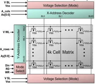
ETUPThe 4kbit array is composed by four architectural blocks, as depicted in Fig. 1: the 1T-1R RRAM cells matrix, a wordline (WL) address decoder, a bitline (BL) address decoder, and the operation control circuitry. The 1T-1R memory cells in the array are constituted by a select NMOS transistor manufactured with a 0.25 µm BiCMOS technology whose drain is in series to a MIM stack. The current compliance is defined through the WL voltage, which allows setting the gate voltage of the NMOS transistor. The cross-sectional Scanning Transmission Electron Microscopy (STEM) image of a 1T-1R cell and the cell schematic are
Implications of the Incremental Pulse and
Verify Algorithm on the Forming and Switching
Distributions in RERAM Arrays
Felice Crupi, Senior Member, IEEE, Francesco Filice, Alessandro Grossi, Cristian Zambelli, Member,
IEEE, Piero Olivo, Eduardo Perez and Christian Wenger
R
reuse of any copyrighted component of this work in other works.
This is the accepted version of the paper. The published version can be found at http://ieeexplore.ieee.org/document/7523250/ The DOI of the published version is: 10.1109/TDMR.2016.2594119
reported in Fig. 2. The variable MIM resistor is composed by 150 nm TiN top and bottom electrode layers deposited by
Fig 1. Block diagram of the memory array.
(a)
(b)
Fig. 2. Cross-sectional STEM image (a) and schematic (b) of the 1T-1R cell integrated in the arrays.
magnetron sputtering, a 7 nm Ti layer, and 8 nm HfO2 layer deposited with an Atomic Vapour Deposition (AVD) process resulting into a polycrystalline HfO2 film. The resistor area is equal to 0.4 μm2. The Forming/Set/Reset operations on the arrays were performed by using an IPV algorithm, as sketched in Fig. 3. The sourceline (SL), BL and WL voltages applied during Forming, Set, Reset and Read operations are reported in Table I. Reset operations were performed by applying the highest WL voltage available (VWL=2.8 V) to maximize the cell switching yield while avoiding the breakdown of the MIM [1]. Pulses were applied during Forming by increasing VBL with ∆VBL=0.01V, whereas during Set and Reset ∆VBL=0.1V and ∆VSL=0.1V have been used, respectively. Forming was done with smaller step compared to Set/Reset in order to have the highest cell-to-cell uniformity after Forming. However, using such step in Set/Reset would drastically increase the cycling time, hence a larger step was used on Set/Reset. Each pulse featured a duration of 10µs, with a rise/fall time of 1µs to avoid overshoot issues. Forming and Set operation were stopped on a cell when the read-verify current reached a value higher than 20μA, whereas Reset was stopped when a value lower than 10μA was reached. The measurement system continued to read all the cells until all the cells reached the stop condition. In other words, for each cycle, the cells which
didn’t reach the stop condition were pulsed and read, while the cells which reached the stop condition were only read.
Fig. 3. IPV algorithm scheme.
III. R
ESULTS ANDD
ISCUSSIONFig. 4(a) and (b) show the histogram of the Forming voltage and the corresponding cumulative distribution function (cdf) in a normal probit scale, respectively. Since the algorithm starts from 2 V, values of Forming voltage lower than 2 V are cumulated in the first bin of the histogram. Unless the first bin, the histogram exhibits a normal shape. The normal distribution in the explored voltage interval, ranging from 2V to 3.2 V, is clearly confirmed by the linear behavior observed in Fig. 4(b).
Fig. 4. Histogram of the forming voltage (a) and the corresponding cdf (b) in a normal probit scale. A normal distribution is observed in the explored voltage range. 2.0 2.2 2.4 2.6 2.8 3.0 3.2 0 100 200 300 400 500 600 700 Forming Voltage (V) Numb er of Even ts Maximum Voltage Minimum Voltage (a) 2.0 2.2 2.4 2.6 2.8 3.0 3.2 -4 -3 -2 -1 0 1 2 3 4 Maximum Voltage Probi t Forming Voltage (V) Minimum Voltage (b) TABLEI
FORMING,SET,RESET AND READ PARAMETERS Operation VSL [V] VBL [V] VWL [V]
Forming 0 2→3.2 1.5
Set 0 0.2→3.2 1.5
Reset 0.2→3.2 0 2.8
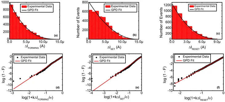
Fig 5. Histogram of the initial distribution of the Forming (a), Set (b), Reset (c) current shift and the corresponding cumulative distribution function (d,e,f). The observed linear behaviors of the cdf confirm that the three initial distributions follow a GPD.
Two distributions for the Forming, Set and Reset current were analyzed. The initial distribution was obtained by considering the values of the current exactly when the stop condition was reached. The final distribution was obtained by considering the values of the current at the end of the programming procedure. Therefore, in the case of the final distribution, almost all the cells were read several times after the stop condition was reached. As it will be shown in the following, the final distribution is significantly different from the initial distribution due to read-induced fluctuations.
In the case of the initial distribution, we considered the shift between the measured current and the threshold current of the IPV algorithm, as follows
∆𝐼𝐹𝑂𝑅𝑀𝐼𝑁𝐺= 𝐼𝐹𝑂𝑅𝑀𝐼𝑁𝐺− 𝐼𝑇𝐻(𝐹𝑂𝑅𝑀𝐼𝑁𝐺) (1)
∆𝐼𝑆𝐸𝑇= 𝐼𝑆𝐸𝑇− 𝐼𝑇𝐻(𝑆𝐸𝑇) (2)
∆𝐼𝑅𝐸𝑆𝐸𝑇 = 𝐼𝑇𝐻(𝑅𝐸𝑆𝐸𝑇) − 𝐼𝑅𝐸𝑆𝐸𝑇 (3)
where ITH(FORMING)=ITH(SET)=20A, ITH(RESET)=10A. As shown in Fig.5, the initial distributions of the Forming, Set and Reset current shift exhibit a monotonic decreasing behavior, which is well fitted by a generalized Pareto distribution (GPD). It is worth noting that the simple exponential distribution fails to fit the experimental data (see Fig. 6).
The probability density function (pdf) and the cdf of the GPD, with shape parameter k≠0, scale parameter , and threshold parameter , are given respectively by
𝑓 =1 𝜎(1 + 𝑘 𝑥−𝜃 𝜎 ) −1−1 𝑘 (4) 𝐹 = 1 − (1 + 𝑘𝑥−𝜃 𝜎 ) −1𝑘 (5)
Fig. 6. The initial distribution of the Forming (a), Set (b), Reset (c) current shift do not follow an expoential distribution, as highlighted by the deviation of experimental data (symbols) by the linear behavior (red line).
0.0 5.0µ 10.0µ 15.0µ 0 200 400 600 800 1000 N u mb e r o f Ev e n ts (a) Experimental Data GPD Fit IFORMING (A) 0.0 5.0µ 10.0µ 15.0µ 0 200 400 600 800 N u mb e r o f Ev e n ts (b) Experimental Data GPD Fit ISET (A) 0.0 3.0µ 6.0µ 9.0µ 0 200 400 600 800 1000 1200 (c) Experimental Data GPD Fit N u mb e r o f Ev e n ts IRESET (A) -3 -2 -1 0 -12 -10 -8 -6 -4 -2 0 Experimental Data GPD Fit log ( 1 F) log(1+kIFORMING/) (d) -4 -3 -2 -1 0 -12 -10 -8 -6 -4 -2 0 (e) Experimental Data GPD Fit log ( 1 F) log(1+kISET/) -2 -1 0 -10 -8 -6 -4 -2 0 (f) Experimental Data GPD Fit log ( 1 F) log(1+kIRESET/) 0.0 2.0µ 4.0µ 6.0µ 8.0µ 10.0µ 0 2 4 6 8 (c) -log(1-F) IRESET (A) 0.0 5.0µ 10.0µ 15.0µ 0 2 4 6 8 -log(1-F) ISET (A) (b) 0.0 5.0µ 10.0µ 15.0µ 0 2 4 6 8 (a) -lo g(1-F) IFORMING (A)
for x>, when k>0, or for x<-/k, when k<0. The first two moments are related to the three GPD parameters (k, , ) by the following equations
𝑚𝑒𝑎𝑛 = 𝜃 + 𝜎
1 − 𝑘 𝑘 < 1
𝑣𝑎𝑟𝑖𝑎𝑛𝑐𝑒 = 𝜎
2
(1 − 𝑘)2(1 − 2𝑘) 𝑘 < 1/2
Obviously, since we considered current shift values as defined by (1)-(3), the threshold parameter is equal to 0 in all cases. By using the maximum likelihood estimation method, we obtain values for the shape parameter k equal to -0.257 (Set), -0.322 (Set) and -0.282 (Reset), and values for the scale parameter equal to 3.88 A (Forming), 4.76 A (Set) and 2.81 A (Reset).
Fig. 7 shows an example of read variability of Forming current measured after the stop condition was reached. We observe that some values of the read current are lower than the threshold current of the IPV algorithm. Similar problems of read instability have been observed also for Set and Reset current (not shown). Read variability has been ascribed to numerous physical mechanisms such as disturbs induced by the read electric field, capture and emission of trapped electrons, and diffusion of traps or vacancies [27].
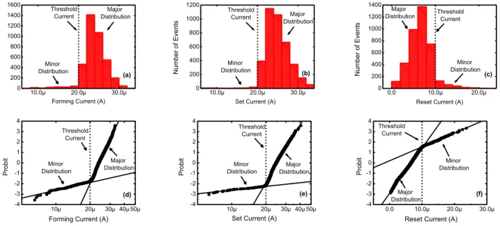
Due to read variability, the GPD evolves to a bimodal distribution for all cases (see Fig. 8). The cdf exhibits a dual slope linear behavior in the lognormal probit scale for Forming and Set and in the normal probit scale for Reset. The separation between the major and the minor distribution is highlighted by the change of slope. As expected, the separation value corresponds to the threshold current of the IPV algorithm: 20 A for Forming and Set and 10 A for Reset.
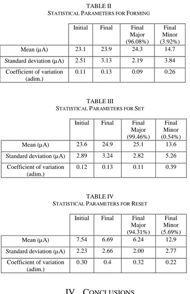
Tables II-IV compare the basic statistical parameters (mean, standard deviation and their ratio, referred as coefficient of
variation) for the initial and the final distribution of Forming, Set and Reset, respectively. In the case of the final distribution, the statistical parameters for the major and the minor distribution are also reported. The main difference between the initial and the final distribution is clearly the appearance of the unwanted minor distribution, which does not respect the algorithm stop condition. The percentage of the minor distribution is in the order of a few percentage points for Forming and Reset and lower than 1% for Set. In other words, the use of different thresholds for Set and Reset in the IPV algorithm does not guarantee the absence of overlap between the two populations, due to fluctuations induced by the readings occurring after the cell programming. On the one hand, the mean value of the final distribution for Set and Reset is better respect to the initial distribution, since it is higher for Set and lower for Reset. On the other hand, the standard deviation and the coefficient of variation of the final distribution for Set and Reset are worst (higher) respect to the initial distribution.
Fig. 7. Read variability of Forming current after the stop condition was reached.
Fig 8. Histogram of the final distribution of the Forming (a), Set (b), Reset (c) current and the corresponding cumulative distribution function (d,e,f). A clear bimodal distribution is observed in all cases.
0 20 40 60 80 100 10 15 20 25 30 Read Curr ent ( A ) Number of Readings Threshold Current 10.0µ 20.0µ 30.0µ 0 200 400 600 800 1000 1200 1400 1600 Numb er of E vent s (a) Threshold Current
Forming Current (A) Minor Distribution Major Distribution 10.0µ 20.0µ 30.0µ 0 200 400 600 800 1000 1200 Numb er of E vent s (b)
Set Current (A) Minor Distribution Major Distribution Threshold Current 0.0 10.0µ 20.0µ 0 200 400 600 800 1000 1200 1400 Numb er of E vent s (c)
Reset Current (A) Threshold Current Minor Distribution Major Distribution 10µ 20µ 30µ 40µ 50µ -4 -3 -2 -1 0 1 2 3 4 (d) Probi t
Forming Current (A) Minor Distribution Major Distribution Threshold Current 10µ 20µ 30µ 40µ 50µ -4 -3 -2 -1 0 1 2 3 4 (e) Probi t
Set Current (A) Minor
Distribution Major Distribution
Threshold Current 0.0 10.0µ 20.0µ 30.0µ -4 -3 -2 -1 0 1 2 3 4
Reset Current (A) (f) Minor Distribution Major Distribution Prob it Threshold Current
IV. C
ONCLUSIONSIn this paper, we have analyzed the implications of the incremental pulse and verify (IPV) algorithm on the Forming and switching distributions of 4kbit RERAM arrays with Ti/HfO2/Ti/TiN stack.
It is shown that the IPV algorithm causes an initial generalized Pareto distribution (GPD) for Forming, Set and Reset current. The threshold current fixed by the IPV algorithm coincides with the GPD threshold parameter. This value is the maximum probability point of the pdf, which exhibits a monotonic decrease for higher (lower) values in the case of Forming and Set (Reset).
Due to read-induced fluctuations, the GPD evolves to a bimodal distribution for all cases. The separation value between the two distributions coincides with the threshold current of the IPV algorithm. The main difference between the initial and the final distribution is the appearance of the unwanted minor distribution, which does not respect the algorithm stop condition. The percentage of the minor distribution is in the order of a few percentage points for Reset and an order of magnitude lower for Set. Moreover, the final distribution exhibits higher values of standard deviation and coefficient of variation for all cases. This experimental study points out that the initial control of the LRS and HRS obtained
by the IPV algorithm is significantly degraded by successive reading
-
induced fluctuations.R
EFERENCES[1] B. D. Salvo, Silicon Non-Volatile Memories: Paths of Innovation. WileyISTE, 2009.
[2] R. Waser, Nanoelectronics and Information Technology: Advanced
Electronic Materials and Novel Devices. Wiley-VCH, 2012.
[3] S. Tanachutiwat, M. Liu, and W. Wang, “FPGA Based on Integration of CMOS and RRAM,” in IEEE Trans. on Very Large Scale Integration
(VLSI) Systems, vol. 19, no. 11, pp. 2023–2032, Nov 2011.
[4] D. Garbin et al., “HfO2-Based OxRAM Devices as Synapses for Convolutional Neural Networks,” in IEEE Trans. on Electron Devices, vol. 62, no. 8, pp. 2494–2501, Aug 2015.
[5] C. Zambelli et al., “Statistical analysis of resistive switching characteristics in ReRAM test arrays,” in IEEE Int. Conf. on
Microelectronics Test Structures (ICMTS), Mar 2014, pp. 27–31.
[6] C. Zambelli et al., “Electrical characterization of read window in ReRAM arrays under different SET/RESET cycling conditions,” in
IEEE Int. Memory Workshop (IMW), May 2014, pp. 1–4.
[7] D.H. Kwon, K.M. Kim, J.H. Jang, J.M. Jeon, M.H. Lee, G.H. Kim, X.S. Li, G.S. Park, B. Lee, S. Han, M. Kim, and C.S. Hwang, “Atomic structure of conducting nanofilaments in TiO2 resistive switching memory,” Nature Nanotechnol., vol. 5, pp. 148–153, Feb. 2010. [8] L.M. Procel, L. Trojman, J. Moreno, V. Maccaronio, F. Crupi, R.
Degraeve, L. Goux, E. Simoen, “Experimental evidence of the quantum point contact theory in the conduction mechanism of bipolar HfO2-based resistive random access memories”, Journal of Applied Physics, vol. 114, 074509, 2013.
[9] P. Lorenzi, R. Rao, and F. Irrera, “Forming kinetics in HfO2-based RRAM cells,” IEEE Trans. on Electron Devices, vol. 60, no. 1, pp. 438– 443, 2013.
[10] N. Raghavan et al., “Statistical insight into controlled forming and forming free stacks for HfOx RRAM,” in Microelectron. Eng., vol. 109, pp. 177–181, Sep. 2013.
[11] D. C. Gilmer et al., “Effects of RRAM stack configuration on forming voltage and current overshoot,” in Proc. 3rd IEEE Int. Memory
Workshop (IMW), May 2011, pp. 1–4.
[12] S.-S. Sheu et al., “A 4 Mb embedded SLC resistive-RAM macro with 7.2 ns read-write random-access time and 160 ns MLC-access capability,” in ISSCC Dig. Tech. Papers, Feb. 2011, pp. 200–202. [13] T.-Y. Liu et al., “A 130.7 mm2 2-layer 32 Gb ReRAM memory device
in 24 nm technology,” in ISSCC Dig. Tech. Papers, Feb. 2013, pp. 210– 211.
[14] S. Yu, X. Guan, and H.-S. P. Wong, “On the switching parameter variation of metal oxide RRAM—Part II: Model corroboration and device design strategy,” in IEEE Trans. Electron Devices, vol. 59, no. 4, pp. 1183–1188, Apr. 2012.
[15] A. Chen and M.-R. Lin, “Variability of resistive switching memories and its impact on crossbar array performance,” in Proc. IEEE Int. Rel.
Phys. Symp. (IRPS), Apr. 2011, pp. MY.7.1-MY.7.4.
[16] A. Grossi et al., “Impact of Intercell and Intracell Variability on Forming and Switching Parameters in RRAM Arrays,” in IEEE Trans. on
Electron Devices, vol. 62, no. 8, pp. 2502–2509, Aug 2015.
[17] A. Grossi et al., “Relationship among current fluctuations during forming, cell-to-cell variability and reliability in RRAM arrays,” in
IEEE Int. Memory Workshop (IMW), May 2015, pp. 1–4.
[18] A. Grossi et al., “Electrical characterization and modeling of pulse-based forming techniques in RRAM arrays,” in Solid-State Electronics, vol. 115, Part A, pp. 17 – 25, 2016. [Online]. Available: http://www.sciencedirect.com/science/article/pii/S0038110115002828 [19] K. Higuchi, T. O. Iwasaki, and K. Takeuchi, “Investigation of verify
programming methods to achieve 10 million cycles for 50 nm HfO2 ReRAM,” in Proc. 4th IEEE Int. Memory Workshop (IMW), May 2012, pp. 1–4.
[20] G. Wang, S. Long, Z. Yu, M. Zhang, Y. Li, D. Xu, H. Lv, Q. Liu, X. Yan, M. Wang, X. Xu, H. Liu, B. Yang, M. Liu, “Impact of program/erase operation on the performances of oxide-based resistive switching memory”, Nanosc. Res. Lett., vol. 10, no. 1, pp. 1–7, Feb. 2015
TABLEII
STATISTICAL PARAMETERS FOR FORMING Initial Final Final
Major (96.08%) Final Minor (3.92%) Mean (A) 23.1 23.9 24.3 14.7
Standard deviation (A) 2.51 3.13 2.19 3.84 Coefficient of variation
(adim.)
0.11 0.13 0.09 0.26
TABLEIII
STATISTICAL PARAMETERS FOR SET Initial Final Final
Major (99.46%) Final Minor (0.54%) Mean (A) 23.6 24.9 25.1 13.6
Standard deviation (A) 2.89 3.24 2.82 5.26 Coefficient of variation
(adim.)
0.12 0.13 0.11 0.39
TABLEIV
STATISTICAL PARAMETERS FOR RESET Initial Final Final Major (94.31%) Final Minor (5.69%) Mean (A) 7.54 6.69 6.24 12.9
Standard deviation (A) 2.23 2.66 2.00 2.77 Coefficient of variation
(adim.)
[21] F. M. Puglisi, C. Wenger and P. Pavan, "A Novel Program-Verify Algorithm for Multi-Bit Operation in HfO2 RRAM", in IEEE Electron Device Letters, vol. 36, no. 10, pp. 1030-1032, Oct. 2015.
[22] A. Belmonte, A. Fantini, A. Redolfi, M. Houssa, M. Jurczak, L. Goux, "Optimization of the write algorithm at low-current (10µA) in Cu/Al2O3-based conductive-bridge RAM", 2015 45th European Solid State Device Research Conference (ESSDERC), Graz, 2015, pp. 114-117.
[23] L. Larcher et al., “A compact model of program window in HfOx RRAM devices for conductive filament characteristics analysis,” in
IEEE Trans. Electron Devices, vol. 61, no. 8, pp. 2668–2673, Aug.
2014.
[24] F. M. Puglisi et al., “An empirical model for RRAM resistance in low and high-resistance states,” in IEEE Electron Device Lett., vol. 34, no. 3, pp. 387–389, Mar. 2013.
[25] S. Balatti et al., “Understanding pulsed-cycling variability and endurance in HfOx RRAM,” in IEEE Int. Reliability Physics Symposium
(IRPS), pp.5B.3.1-5B.3.6, 19-23 April 2015.
[26] S. Deora, G. Bersuker, K. Matthews, D.C. Gilmer, P.D. Kirsch, “AC Variability and Endurance Measurement Technique for Resistive Switching Memories,” IEEE Trans. on Device Mater. Rel.s, vol. 14, no. 1, pp. 300–303, March 2014.
[27] T. O. Iwasaki, S. Ning, K. Takeuchi, “Stability Conditioning to Enhance Read Stability 10x in 50nm AlxOy ReRAM”, IEEE International Memory Workshop (IMW), 2013, pp. 43-47, 2013.