Abstract
SiGe BiCMOS semiconductor technology has been increasing its application domain especially for the development of complex microwave monolithically integrated circuits (MMIC) required for modern telecommunication systems. This thesis presents a set of building blocks developed in different SiGe BiCMOS technologies for reconfigurable antenna applications. The developed blocks are oriented to the implementation of electronically scanned phased arrays or of switched beam antenna systems. The red thread that links the different topics is the next generation mobile communication systems, namely 5G systems. However, 5G networks instead of providing specific requirements for each block are employed as an application context that is adopted to provide a real employment scenario for each device proposed in this work.
The thesis is organized as follows. In the first chapter, an overview about development opportunities of 5G technology is illustrated. In the second chapter, a brief introduction in the world of MMIC and SiGe technology has been provided. In the third chapter, beam-forming networks are dealt introducing the design of an 8x8 Butler matrix and a Wilkinson combiner/divider in SiGe BiCMOS technology. In the fourth chapter, a quarter wavelength resonant filter phase shifter is presented. An innovative technique to realize a phase shifter using the peculiarity of the pass-band filters. In the fifth chapter, it is presented a study on metamaterial structures based on Split Ring Resonators integrated with on-chip Coplanar Wave guides. In the last chapter, a FDD technique is illustrated along with the design of a Duplexer in K/Ka-band with High/Low pass filter.
Table of contents
Abstract ... 2
Table of contents ... 3
... 6
...12
Technical characteristics for 5G mobile communications systems ... 13
Fundamentals on 5G ... 15
MMIC and SiGe BiCMOS technology ... 18
Monolithic Microwave Integrated Circuit ... 18
BiCMOS technology ...21
Antenna array beam forming networks ... 23
Butler Matrix and a switched array system ... 24
Butler Matrix: state of the art... 27
Design of an 8x8 BiCMOS Butler Matrix ... 30
3.3.1 Hybrid coupler: theory and different topologies evaluation ... 31
3.3.2 Hybrid coupler design ... 36
3.3.3 Phase delay line ... 40
3.3.4 Crossover ...41
3.3.5 Simulation results ... 42
3.3.6 Measurement setup and final results ... 44
Wilkinson power divider ... 52
Wilkinson power divider state of art ... 53
Design of a multi Stage WPC/D ... 55
3.6.1 Schematic ... 56
3.6.2 Layout ... 58
3.6.3 Comparison of measurements and simulations ... 59
Phase shifter ... 63
Phase shifter classification ... 63
Phase shifter state of art ... 67
Quarter Wavelength Reflect Type Phase Shifter ... 71
4.3.1 Quarter-wavelength transmission lines design ... 73
4.3.2 LC resonator and varactor diode design ... 74
4.3.3 Simulation and measurements results of QWRF PS ... 81
Metamaterials transmission line loaded with a Split Ring Resonator ... 85
Metamaterials transmission line ... 86
Metamaterials filters ... 89
Split Ring Resonator state of art ... 91
Design of capacitively-loaded Split Ring Resonators transmission line filters 92 5.4.1 SRR Coplanar Waveguide ... 93
5.4.2 SRR-CPW equivalent circuit ... 94
5.4.4 Capacitively Loaded Split Ring Resonator (SRR) ... 96
5.4.5 New configuration of the capacitively loaded Split Ring Resonator (SRR) 98 5.4.6 Capacitive Loaded Split Ring Resonator (SRR) with integration of the varactor ... 102
Duplexer for SAT-COM On-the-Move application ... 105
Duplexer state of art ... 106
Design of a duplexer for SAT-COM On-the-Move application ... 108
6.2.1 Measurement and simulation comparison ... 112
6.2.2 Comparison with the state of art ... 115
Conclusions ... 116
Figure 1-1 Possible solutions for MMB architecture. ...14
Figure 1-2 5G system architecture ... 15
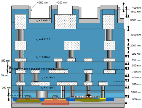
Figure 2-1 IHP SiGe BiCMOS SG25H3 stack-up with upper part for passive and the bottom part for active device. ... 19
Figure 2-2 SiGe wafer ...21
Figure 3-1 (a) Analog phased array system, (b) switched array system ... 23
Figure 3-2 Block diagram of a 4x4 Butler matrix ... 25
Figure 3-3 Simultaneous radiation patterns of phased array connected to an 8x8 Butler matrix. ... 27
Figure 3-4 Die photograph of the 4-way CMOS Butler matrix [13] ... 28
Figure 3-5 Microphotograph of the proposed Butler matrix in [14]... 28
Figure 3-6 Die photograph of the 4x4 CMOS Butler matrix presented in [15] . 29 Figure 3-7 Microphotograph of the 8x8 Butler matrix [13] ... 30
Figure 3-8 Block diagram of a 8x8 Butler matrix ... 30
Figure 3-9 Ideal transformer ... 32
Figure 3-10 Non-ideal transformer: physical model ... 33
Figure 3-11 Tapped transformers ... 34
Figure 3-12 Stacked transformer ... 34
Figure 3-13 Interleaved transformer ... 35
Figure 3-14 Quadrature coupler equivalent circuit ... 35
Figure 3-15 ST BiCMOS9MW BEOL Stack-up ... 37
Figure 3-16 Designed interleaved transformer: (a) Top view (b) Top view (zoom) (c) side view (d) table with the values geometrical parameters. ... 38
Figure 3-17 Simulated transmission parameter and output phase deviation of the
quadrature hybrid ... 39
Figure 3-18 45° Delay line: (a) layout (b) Output phase. ...41
Figure 3-19 Crossover isolation ... 42
Figure 3-20 Simulated input return loss of Butler matrix ... 42
Figure 3-21 Simulated input insertion loss of Butler matrix ... 43
Figure 3-22 Final layout of the 8x8 Butler matrix ... 43
Figure 3-23 Transmission Phase (a) Simulated radiation pattern using all input ports (b) ... 44
Figure 3-24 Submitted (left) and manufactured (right) layout of the 8x8 BiCMOS Butler matrix ... 44
Figure 3-25 PCB test board section. ... 45
Figure 3-26 Butler matrix integrated in a PCB board by wire bonding ... 45
Figure 3-27 Butler matrix integrated in a PCB board, zoom to the chip area and wire bonding ... 46
Figure 3-28 PCB designed test boards of Butler Matrix and Hybrid Coupler. It has been designed de-embedding circuit for the connector and for each branch of the BM and Hybrid Coupler... 47
Figure 3-29 De-embedded measurement of Insertion Loss from all input ports trough all output of the Butler matrix ... 47
Figure 3-30 De-embedded measurement of input and output return loss of the Butler Matrix. ... 48
Figure 3-31 De-Embedded measurement of output phase distribution of the Butler matrix fed though different input ports ... 48
Figure 3-32 Simulated 24 GHz array factor based on the de-embedded measurement of the Butler matrix with isotropic antenna elements ... 49
Figure 3-33 Post measurements study on the test board: ADS representation of
part of the board including coupling effect of wire bonding and microstrip ... 50
Figure 3-34 Possible solution for a future test board design with SMD connector ... 51
Figure 3-35 RX chip of a SAT-COM on the move application ... 52
Figure 3-36 General Wilkinson combiner ... 53
Figure 3-37 Schematic of the lumped-element equivalent circuit of the line section (left) and Microphotograph (right) of the WPD presented in [24] ... 54
Figure 3-38 Schematic (left) and Microphotograph (right) of the four way WPD presented in [25] ... 54
Figure 3-39 The prototypes of the proposed CMOS WPD using synthetic transmission lines ... 55
Figure 3-40 Distributed element Wilkinson combiner/divider ... 56
Figure 3-41 Distributed element WPD ... 56
Figure 3-42 Return loss of 20 GHz (red line) and 30 GHz (blue line) WPD ... 57
Figure 3-43 Schematic of 2 stages WPD... 58
Figure 3-44 Final layout of a 30GHz Wilkinson combiner/divider ... 59
Figure 3-45 Wilkinson combiner on chip measurement setup... 59
Figure 3-46 Simulation (blue) vs measurement (red) results of Tx Wilkinson combiner ... 60
Figure 3-47 Simulation (blue) vs measurement (blue) results of Rx Wilkinson combiner ... 61
Figure 4-1 Beam Forming network TX architecture ... 63
Figure 4-2 PS with constant phase ... 66
Figure 4-4 (a) QWRF-PS simple model. (b) Amplitude and phase transmission responses of a QWRF-PS obtained with the varactor diodes biased to achieve the
lowest (solid line) and highest (dashed line) capacitance values [30]. ... 71
Figure 4-5 Single cell results swiping C and keeping L fixed (@23.5 GHz) ... 72
Figure 4-6 (a) Schematic model of QWRF-PS (b) Lumped elements transmission line (c) Simplified varactor model ... 73
Figure 4-7 (a) HFSS layout of a lumped elements λ/4 transmission lines and (b) simulation results of Phase delay and S-Parameter ... 74
Figure 4-8 (a) Symbol, (b) equivalent circuit and (c) C-V characteristic of a varactor diode ... 76
Figure 4-9 C-V curve of a varactor done by 1 or 2 diodes ... 77
Figure 4-10 Full schematic of a 23GHz PN junction varactor for QWRF PS ... 78
Figure 4-11 C-V curve of the designed varactor at 23.5 GHz ... 79
Figure 4-12 Quality factor performance versus 𝑉𝐷𝐶 ... 80
Figure 4-13 Plot of 𝑆11 on the Smith Chart of the proposed Varactor ... 80
Figure 4-14 (a) Submitted layout and a (b) microphotograph picture of the QWRF-PS ... 81
Figure 4-15 Sim. (solid) and Meas. (dashed) of insertion loss versus bias voltage ... 82
Figure 4-16 Simulation (solid) and Measurement (dashed) return loss versus bias voltage ... 82
Figure 4-17 Simulation (solid) and Measurement (dashed) phase shift and RMS error phase. ... 83
Figure 4-18 Simulation (solid) and measurement (dashed) of amplitude transmission responses of a QWRF-PS obtained varying varactor diodes voltage feeding ... 83
Figure 5-1 Metamaterials classification according the signs of 𝜀 and µ ... 85 Figure 5-2 Equivalent circuit model of transmission line (a) Conventional RH transmission line. (b) Dual LH transmission line.(source [42]) ... 87 Figure 5-3 Unit-cell equivalent T-circuit models of the transmission lines according to the sign of the series reactance and shunt suscepetance. (source [42]) ... 89 Figure 5-4 SiGe BiCMOS Split Ring Resonator (SRR) loaded Coplanar Waveguide (CPW) geometry: a) SiGe BiCMOS stack up; b) SRR (TM1) and CPW (TM2) geometrical parameters. ... 93 Figure 5-5 Equivalent circuit of the SRR loaded CPW line ... 94 Figure 5-6 SRR-CPW line unloaded pass-band filter: simulated ... 96 Figure 5-7 Capacitively loaded CPW-SRR line. MIM capacitor between the outer SRR gap ... 97 Figure 5-8 Miniaturized loaded CPW-SRR line: full wave simulated results. ... 98 Figure 5-9 CPW loaded SRRs with lumped capacitors: (a) MIM capacitors shown in the top view; (b) size view including the vertical interconnections from the MIM capacitors, the CPW ground, and the SRRs. ... 99 Figure 5-10 Equivalent circuit of the CPW line and the loaded SRRs. ... 100 Figure 5-11 Simulated equivalent circuit and full-wave scattering parameters of the unit cell. ... 101 Figure 5-12 CPW loaded SRRs with lumped capacitors (𝐶𝐵𝑡𝑤𝑛) ... 102 Figure 5-13 Final layout of SRR CPW and frequency shift changing 𝐶𝐵𝑡𝑤𝑛 ... 103 Figure 5-14 C-V curve and Q-V curve of the varactor designed for the SRR CPW ... 103 Figure 5-15 Schematic e return loss of the SRR CPW with varactor ... 103
Figure 6-1 General architecture of a Ka band chip with 6 core (4 Tx and 2 Rx) ... 108 Figure 6-2 Design of the duplexer using HI/LOW pass filter ... 109 Figure 6-3 Duplexer equivalent circuit. (a) Schematic and (b) layout optimized. ... 110 Figure 6-4 Top view and 3D view of the final layout of the designed duplexer. 111 Figure 6-5 HFSS simulation results of the designed duplexer ... 112 Figure 6-6 Microphotograph picture of the duplexer ... 113 Figure 6-7 Measured and simulated results of the designed duplexer ... 114
Table 3-1 Phase distribution of an 8x8 Butler matrix ... 31
Table 3-2 Inductance and capacitance needed for phase delay ... 40
Table 3-3 Specification set of WPDs designed for SAT-COM on the move application ... 55
Table 3-4 Lumped element values of a WPD designed at 20GHz and 30 GHZ . 57 Table 3-5 Comparison the major characteristics of the proposed Wilkinson power combiners and other works ... 62
Table 4-1- State of art of analog phase shifter ... 68
Table 4-2 - State of art of digital phase shifter ... 69
Table 4-3 - Typical qualitative performance of integrated phase shifter approaches. TL: transmission lines, LP: low-pass filter, HP: high-pass filter, gm: trans-conductance, Z: impedance, L: inductance [29]. ... 70
Table 4-4 Design component values of QWRF PS ... 81
Table 4-5 Comparison of tunable phase shifters ... 84
Table 5-1 SRR CPW line dimensions ... 95
Table 5-2 Equivalent Circuit Parameters ... 101
Table 6-1 Comparison of designed Wilkinson Power combiner/divider with the state of art ... 115
Technical characteristics for 5G mobile
communications systems
A 7-fold increase of the worldwide mobile traffic is expected between 2016 and 2021. This rate will soon go beyond the capacity of currently available mobile communication networks thus demanding a new high-capacity system which is referred to as 5G [1]. Researchers around the world are exploring possible ideas and technologies for the fifth-generation mobile networks (5G). Many cases of use have been summarized in various white papers and reveal demanding requirements. The possible technologies and ideas under discussion to meet these requirements are very different. There is no doubt that there is a need to improve the understanding of any new air interface at frequencies above existing cellular network technologies, from 6 GHz up to 100 GHz, as well as advanced antenna technologies such as massive MIMO and beam forming.
The current fourth generation for mobile communications already use advanced technology, such as orthogonal frequency division multiplexing (OFDM) or multiple input multiple output (MIMO), in order to achieve spectral efficiency close to theoretical limits in terms of bits per second per Hertz per cell [2]. One possibility to increase capacity per geographic area is to deploy many smaller cells such a femtocells and heterogeneous networks. However, because capacity can only scale linearly with the number of cells, small cells alone will not be able to meet capacity required to accommodate orders of magnitude increases in mobile data traffic. As the mobile data demand grows, the sub-3GHz spectrum is becoming crowded. On the other hand, a vast amount of spectrum in the 3-300GHz range remains underutilized. This portion of spectrum is called millimeter-wave band. Millimeter-wave communications system that can achieve
multi-gigabit data rates at a distance of up to a few kilometers already exist for point-to point communications. However, the electronics component used in this field are too big in size and consume too much power to be applied in mobile communications. In order to ensure good coverage MMB (millimeter-wave mobile broadband) base stations need to be deployed with higher density than macro-cellular base stations. The transmission and reception in an MMB system are based on narrow beams, which suppress the interference from neighboring MMB base stations and extend the range of an MMB link. This allows significant overlap of coverage among neighboring base stations. Unlike cellular systems that partition the geographic area into cells with each cell served by one or a few base stations, the MMB base stations form a grid with a large number of nodes to which an MMB mobile station can attach. For example, with a site-to-site distance of 500m and a range of 1 km for an MMB link, an MMB mobile station can access up to 14MMB base stations on the grid, as shown in Figure 1-1.
Figure 1-1 Possible solutions for MMB architecture.
This possible solution has the advantage to eliminate the problem of poor link quality at the cell edge that is inherent in cellular system and enables high-quality equal grade of service. However, the main disadvantages are related to the cost of
wired network necessary to connect every MMB base station. To avoid the problems related to costs the more attractive solution could be the utilization of some MMB base stations to connect to the backhaul via other MMB base stations.
Figure 1-2 5G system architecture
As illustrated by Figure 1-2, 5G will be a truly converged system supporting a wide range of applications from mobile voice and multi‐Giga‐bit‐per‐second mobile Internet to D2D and V2X (Vehicle‐to‐X; X stands for either Vehicle (V2V) or Infrastructure (V2I)) communications, as well as native support for MTC and public safety applications [1].
Fundamentals on 5G
The 5G is really on the horizon and clearly has a major role in global research and pre-development. Constant demand for higher data rates and faster connections from users require much more wireless network capabilities, especially in high-density areas. The industry expects a 100 times higher data rate per user and a capacity greater than 1000 times, and has defined these goals for the fifth generation mobile network (5G). An example is sports events or concerts, where
many viewers want to share their experience instantly through sharing images or videos. The event itself could also offer additional services to viewers, such as basic information about playing music or replaying to the slower sports sequences.
In addition to the infinite demands for a larger offer, faster data rates at rush hours, greater capacity, better cost efficiency, especially the new Internet Things of Things (IOT), proposes new challenges to face. It is expected that millions of devices will "talk" to each other, including machine-to-machine (M2M), vehicle-to-vehicle (V2V), or general-use x-2-y.
This will require different requirements than those currently faced by 4G systems, which have been optimized to provide access to mobile broadband data. However, not just the number of devices is crucial: high reliability, long battery life (years instead of days) and very short response times (latency) require a further "G" in the future. Reducing energy consumption in cellular networks is another important requirement. This is particularly difficult since peak capacity and speed data must be increased at the same time.
The ongoing research is revealing a series of technological components aimed at achieving ambitious goals, including:
Millimeter waves: Exploring the higher frequency ranges would allow the use of higher bandwidths, which would lead to higher peak data rates and system capabilities.
New air interfaces: The LTE based air interface based on OFDM will not be adequate for some cases of use and therefore a certain number of new air interface candidates is being discussed.
Massive MIMO / Beam forming, active antennas: particularly at higher frequencies, the significant increase in leakage in the propagation path
should be compensated by higher antenna gains. In addition, adaptive beam training algorithms, even on a per-user basis, are needed and can be implemented using active antenna technology.
Device-to-Device Communications (D2D): An already existing use case to meet public security needs through LTE. Implementing D2D communications could also allow low latency for specific scenarios.
Network Virtualization (Cloud Based Network): The goal is to run the current dedicated hardware such as virtualized software functionality on general-purpose hardware in the central network. This is extended to the radio network by separating base stations into radio units and baseband units (i.e. fiber-connected) and gathering baseband units to handle a large number of radio units.
Control of division and user plane and / or decoupling downlink and uplink: the goal is to use heterogeneous networks, making it possible to control all user devices on a macro level, while user data is provided independently by a small cell.
Light MAC and RRM strategies optimized: Considering the high number of potentially very small cells, radio resource management needs to be optimized. Planning strategies would potentially require stack of slower protocols, which could also be used in uncoordinated scenarios.It is significant that the European Research Program 5G is called Horizon 2020. It gives an idea of the timeline foreseen for the dissemination of this new technology[3].
MMIC and SiGe BiCMOS technology
As the frequency of operation of electronic circuits increases, the parasitic impedance plays a major role in the circuit performance. In circuit simulation, these factors are generally neglected. Soldering of the components, leads etc. also contributes to the parasitic effect. Other than performance degradation, circuit repeatability is also lost, as the effect of soldering will not be exactly same for each iteration. To get rid of these effects and to enable higher integration densities, MMIC circuits are used at high frequency.
Monolithic Microwave Integrated Circuit
“Monolithic Microwave Integrated Circuit” (MMIC) are integrated circuits (IC) operating at microwave frequencies (300 MHz to 300 GHz) with active and passive components fabricated on one semiconductor substrate. The term monolithic comes from the possibility to realize passive and active structures not in a planar way, but MMICs offer to the designers several metallization layers as it is shown in Figure 2-1.
In this technology, all the elements are grown on a common wafer. The circuit size is small resulting in negligible parasitic. As no soldering is involved, repeatability of circuit is also achieved.
Therefore, MMIC results in low mass-size, less parasitic and repeatable circuits. Other than active devices, capacitor, inductors and transmission lines are the components mostly involved in any high frequency circuit.
Figure 2-1 IHP SiGe BiCMOS SG25H3 stack-up with upper part for passive and the bottom part for active device.
The manufacturing process of the wafers entails forming micrometric or even nanometric features on their surface. Because of this reason, the fabrication process is costly and time consuming. MMIC technology provides the core components for many applications of microwave and telecommunication. There are some advantages of applying MMIC technology that listed below [4]:
Cheap in large quantities; Good reproducibility; Small;
Light;
Less parasitic; Larger bandwidth.
MMICs were originally fabricated using gallium arsenide (GaAs), a III-V compound semiconductor. It has two fundamental advantages over silicon (Si),
the traditional material for IC realization: device (transistor) speed and a semi-insulating substrate. Both factors help with the design of high-frequency circuit functions. However, the speed of Si-based technologies has gradually increased as transistor feature sizes have reduced, and MMICs can now be fabricated in Si technology. The primary advantage of Si technology is its lower fabrication cost compared with GaAs. Silicon wafer diameters are larger (typically 8" or 12" compared with 4" or 6" for GaAs) and the wafer costs are lower, contributing to a less expensive IC.
The advances in silicon transistor performance from 1998 to 2004, for both the MOSFET and the Silicon Germanium (SiGe) HBT processes, coupled with the high integration density of five to seven metal layers, have allowed high performance MMICs to be developed at microwave and even millimeter-wave (mm-wave) frequencies. For the SiGe technology, the transistor maximum (unity gain) frequency fT in standard commercial runs increased from 40 to50 GHz in
1998 to >200 GHz in 2004. The last ST BICMOS55 has been released with a fT >
300 GHz.
In order to design MMICs, it is necessary to have precise characterization/ modeling of elements (mainly FETs) and impedance analysis based upon it, circuit design suitable to monolithic integration, and element and device fabrication technology appropriate to microwave frequencies and above.
Figure 2-2 SiGe wafer
BiCMOS technology
BiCMOS is a technology for the production of integrated electronic components. The acronym stands for Bipolar Metal Oxide Semiconductor Semi-conductor and indicates the technology that integrates CMOS and BJT on the same semiconductor chip. The advantage of this process is feasible in the various different technologies. The main advantages are derived directly from the advantages of the two families of devices: if on the one hand the MOS has low power consumption and wide noise margins, on the other the bipolar has a greater ability to drive high loads and high gain. Normally, a CMOS circuit, to obtain a suitable fan-out (ability to drive a load), make use of coupling circuits (buffers). Another important advantage is that the overall capacity of a BiCMOS port is almost equal to one of BJT only, so it is very low. This allows a significant increase in the frequency performance of the BiCMOS when used as a broadband amplifier, or in the same way, a significant increase in the switching frequency when used in logic circuits. For example, by incorporating NMOS, PMOS and NPN BJT devices on the same integrated circuit, BiCMOS process technology
offers the promise of hybrid SRAM solutions that combine the low power and high capacity characteristics of CMOS with the fast access and cycle times of bipolar memories. Another important advantage is the possibility of combining in the same integrated analog and digital electronics, which is useful in realizing system-on-a-chip.
Antenna array beam forming networks
Nowadays, wireless communication systems are required to process extremely increasing data with high performance, maximize throughput, and small cell etc. Typically, beam forming can be implemented following two main approaches [5].
- phased array systems Figure 3-1(a) - switched array systems Figure 3-1(b).
Phased array systems are implemented by placing an attenuator and phase shifter in front of each antenna element [6]. This approach allows to fully control the array pattern, but it results in a complex and costly architecture. On the other hand, in the switched array approach the phase of each radiating element can vary only within a given number of states which can be generated by a Rotman lens such as in [7] or [8], a Blass matrix [9] or a Butler matrix [10].
Figure 3-1 (a) Analog phased array system, (b) switched array system
Beam formation networks combine signals from multiple antennas into an array that is more directional than each antenna taken individually. These networks are used both in radars and in mobile communications. An example of radar system that uses a linear array of antennas is the one currently used in automotive environments and capable of generating four azimuth beams or, in remote sensing applications, arrays are used by a satellite to route its beam to the Earth.
Beam-forming networks (BFNs) are the signal distribution systems to the different antenna of an array system. Their main function, therefore, is to distribute the signal according to specific amplitude and phase distribution criteria. Depending on their typology, BFNs can generate a single beam or different radiation pattern configurations [11].
Beam forming networks do offer various advantages over phased arrays the main one being related to the use of passive components which reduce losses while providing a great simplification of the architecture which does not require a phase or amplitude control for each element. As a result, also the power consumption is greatly reduced being limited only to the switching and control elements.
Butler Matrix and a switched array system
The Butler matrix is configured as a multiport system with N inputs and N outputs. The outputs are the input ports of the antennas while the inputs represent different possible configurations of the radiation pattern of the N radiant elements. Depending on which of the N inputs it activates, the antenna beam is guided in a specific direction in a plane; Butler matrices can be combined on two levels and are used to facilitate 3D scanning.
The first approach with this matrix was described in an article [10] published by the people who named this passive component Jesse Butler and Ralph Lowe in 1961.
The main features of Butler's matrix are:
N inputs and N outputs, with N usually varying between 4, 8 or 16. Inputs are isolated from each other.
The N outputs are linear with respect to the position, so the output beam is deviated from the main axis.
None of the inputs provides a very wide beam.
Increasing the phases between outputs depends on which input is used By the way, this is a reciprocal passive network, so it works in the same way both when it transmits energy and when it receives it.
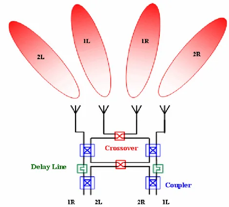
Figure 3-2 shows a block diagram of a typical 4x4 Butler matrix. It usually consists of 2𝑛 inputs and 2𝑛 outputs. Therefore, 𝑁
2log2𝑁 hybrid couplers are
needed, where 𝑁 = 2𝑛 is the number of input/output. The number of delay lines
can vary; in the case of the 4x4 matrix there are 2 phase delays that will provide a shift of 45° of signal. Phase delay of 22.5 ° (x2), 45 ° (x4) and 67.5 ° (x2) are required for an 8x8 matrix.
Outputs are the Fourier transform of inputs and the circuit diagram of a Butler matrix is the same as the FFT (Fast Fourier Transform).
If the Butler matrix is connected to an array of antennas, the array will perform its purpose as a beam former and the array will have a uniform distribution of amplitude and a constant phase difference between adjacent elements:
exp (−𝑗 𝑘 𝑛 𝑑𝑥 𝑢𝑖) with 𝑢𝑖 = ( 𝜆 𝑁 𝑑𝑥) ∗ 𝑖 where 𝑖 = ± ( 1 2 , 3 2 , 5 2 , … ) if N is even and 𝑖 = ±(1,2,3, … ) if N is odd.
The generated radiation patterns are N different beams having different angular directions and covering an angular field of 180 °, see Figure 3-3. The direction of the beams depends on which input is used to introduce the signal while the scanning range depends also on the spacing between the array elements. The phase difference between the radiating elements for a Butler matrix with N elements is given by:
Ψn =2 𝜋 𝑑
𝜆 cos 𝛼 = ±
2 𝑝 − 1
𝑁 𝑥 180°
where the phase difference, Ψn, it’s plus or minus depending on whether the beam
is to the right or left respectively relative to the frontal direction. Since the equation depends on 𝜆 the beam angles u vary with frequency. The Butler matrix, therefore, forms beams whose width depends on frequency. The series of beams generated will be tight at high frequencies and wider at low frequencies [12]
Figure 3-3 Simultaneous radiation patterns of phased array connected to an 8x8 Butler matrix.
Butler Matrix: state of the art
In the literature, there are several techniques of realization of Butler matrices. Among the various types of designs and realizations in this paragraph will be some sample examples of Butler made on-chip.
In [13] a 24-GHz 4-way Butler Matrix MMIC in 0.18-µm CMOS technology is presented. The multi-layer structure of CMOS process is utilized to monolithically realize the bulky Butler matrix on silicon substrate (Figure 3-4). Particularly, the multi-layer bifilar transformer is introduced to miniaturize the circuit and reduce the signal loss. The implemented CMOS Butler matrix MMIC only occupies a chip area of 0.41 𝑚𝑚2 (excluding I/O pads). The experimental
results show that insertion losses are 2.2±0.6 dB from 23 to 25 GHz and the phase errors are within 6°. Therefore, by connecting this Butler matrix to a linear array antenna, four orthogonal beams, pointing to -49°, -15°, 15°, and 49°, respectively, are generated within 0.3° error.
Figure 3-4 Die photograph of the 4-way CMOS Butler matrix [13]
In [7] and [14] A compact V-band 4x4 Butler matrix, using 0.35 μm SiGe bipolar process, is proposed. This design exhibits an average insertion loss of 3 dB with amplitude variation less than 1.5 dB and an average phase imbalance of less than 10° from 55 GHz to 65 GHz. The chip area is only 0.5x0.9 𝑚𝑚2 including all pads.
The SiGe Butler matrix is an excellent candidate for MIMO systems and applied in high data-rate communications.
In [15] a novel design of monolithic 2.5-GHz 4 4 Butler matrix in 0.18- m CMOS technology in proposed. To achieve a full integration of smart antenna system monolithically, the proposed Butler matrix is designed with the phase-compensated transformer-based quadrature couplers and reflection-type phase shifters. The measurements show an accurate phase distribution of 45 ± 3° , 135 ± 4° , −45 ± 3° 𝑎𝑛𝑑 − 135 ± 4° with amplitude imbalance less than 1.5 dB. The antenna beamforming capability is also demonstrated by integrating the Butler matrix with a 1x4 monopole antenna array. The generated beams point towards -45°, -15°, 15°, and 45°, respectively, with less than 1 error, which agree very well with the predictions. This Butler matrix consumes no dc power and occupies the chip area of 1.36x1.47 𝑚𝑚2.
Figure 3-6 Die photograph of the 4x4 CMOS Butler matrix presented in [15]
In [16] and [17] are presented a two miniature 11-13GHz and 5–6-GHz 8x8 Butler matrix in a 0.13- m CMOS implementation. The 8x8 design results in an insertion loss of 3.5 dB at 5.5 GHz and no power consumption. The chip areas are respectively 0.95x0.65 𝑚𝑚2 and 2.5x1.9 𝑚𝑚2 including all pads. The 8x8 matrix
measured patterns agree well with theory and show an isolation of 12 dB at 5–6 GHz.
Figure 3-7 Microphotograph of the 8x8 Butler matrix [13]
Design of an 8x8 BiCMOS Butler Matrix
The ideal block diagram of the designed Butler matrix is shown in Figure 3-8.
Figure 3-8 Block diagram of a 8x8 Butler matrix
The designed Butler matrix is a 16-port component, where 8 ports are used to feed an array of 8 antennas. Depending on the port being fed, the array is excited with different phase distributions and depending on how phases are deployed,
the direction of the main beam varies between -61 and +61 degrees. A summary of the output phase distribution and the associated beam directions are given in Table 3-1.
Table 3-1 Phase distribution of an 8x8 Butler matrix
In this research study, an innovative design of an on-chip 8x8 Butler matrix implemented using a BiCMOS process.
3.3.1 Hybrid coupler: theory and different topologies evaluation
The most important component of a Butler matrix is the quadrature hybrid coupler. Hybrids are 3dB directional couplers with a phase difference of 90° to the outputs of through and coupled branches. This component is the one that takes up more area on the chip. For this reason, specific attention was devoted to the reduction of the size occupied by this sub-block.
An ideal transformer contains 3 main components and Figure 3-9 shown the ideal circuit that represent it.
Figure 3-9 Ideal transformer
𝐿1 and 𝐿2 represents the self-inductance of the primary and secondary coil while
M represents the mutual inductance in between. The terminal voltages and currents of an ideal transformer are specified by the following equations [18].
𝑣1 = 𝐿1𝜕𝑖1 𝜕𝑡 + 𝑀 𝜕𝑖2 𝜕𝑡 𝑣2 = 𝐿2 𝜕𝑖2 𝜕𝑡 + 𝑀 𝜕𝑖1 𝜕𝑡
The mutual inductance, M, is related to the self-inductances, 𝐿1 and 𝐿2, by the
mutual coupling coefficient, k:
𝑘 = 𝑀
√𝐿1𝐿2
As the transformer is a passive device the value of k is ≤ 1. k = 1 means ideal transformer but typical value of on-chip transformers exhibit k values between 0.3-0-9.
Figure 3-10 Non-ideal transformer: physical model
In Figure 3-10, parasitic resistances and capacitances present in the non-ideal transformer are shown. Resistance 𝑅1 and 𝑅2 model the series resistance of the two coils. The spiral-to-substrate oxide capacitances (𝐶𝑜𝑥,1𝑎 etc.) and the
terminal-to-terminal oxide capacitances (𝐶𝑠,𝑖𝑗 with i,j = 1..2) and the resistive and
capacitive losses to the substrate (𝑅𝑠𝑖 and 𝐶𝑠𝑖). The self/mutual inductance and
series resistance are independent of the configuration of the transformer. In literature, mainly 3 types of monolithic transformers can be found:
1. Tapped Transformers; 2. Stacked Transformers; 3. Interleaved Transformers.
The first one is depicted in Figure 3-11 is the best suited for three-terminal applications due to the asymmetry it permits a variety of tapping ratios to be realized.
Figure 3-11 Tapped transformers
The stacked transformer (Figure 3-12) uses multiple layers and thanks to the vertical and lateral coupling provide the best area efficiency, the highest self-inductance and highest coupling (k is typical around 0.9). The main disadvantage of this transformer is the high terminal-to-terminal capacitance that cause a low self-resonance.
Figure 3-12 Stacked transformer
The interleaved transformer is suitable for four-terminal application that demand symmetry. The interleaving of the two inductances permit moderate coupling (k=0.7) to be achieved at the cost of reduced self-inductance. This coupling may be increased at the cost of higher series resistance by reducing the turn width and spacing.
Figure 3-13 Interleaved transformer
Different layouts are available in the state of art and the aim is to maximize the coupling between coils. The solution introduced in this work is based on the latter type of transformer because although the staked transformer allows higher coupling factors, but coils have different electrical parameters because they are built with different metal layers. Interleaved structures provide full symmetry between two coils but in the other side poor magnetic coupling. In a first design approach, it is implemented using the lumped element equivalent network shown in Figure 3-14(a). This simplified model fits well with the interleaved transformer.
Figure 3-14 Quadrature coupler equivalent circuit
The following equations are used to model the transformer, and this is how geometrical parameters are related with the model:
𝐿 =𝜇 𝑛 2 𝑑 𝑎𝑣𝑔 2 [𝑙 𝑛 ( 2.46 𝜌 ) + 0.2 𝜌]
L is the inductance value of the two coils that are identical where 𝜌 =(𝐷𝑜𝑢𝑡−𝐷𝑖𝑛)
(𝐷𝑖𝑛+𝐷𝑜𝑢𝑡)
is the fill factor and 𝑑𝑎𝑣𝑔 = 0.5 (𝐷𝑜𝑢𝑡− 𝐷𝑖𝑛) is the average diameter.
𝑅1,2 = 𝑅𝐷𝐶1,2+ (1 + 0.1 √𝑓 + 0.002 𝑓2 )
𝑅𝐷𝐶1,2 and 𝑅1,2 are the dc and ac series resistances of the coils (𝑅1 and 𝑅2 respectively) and f is the frequency expressed in GHz.
𝐶𝑂𝑋 = 𝐴 𝜀𝑂𝑋
𝑡𝑂𝑋 + 𝑃 𝐶𝑠
The value of Cox (that actually takes into account the substrate effect) arises from
both area and perimeter effects so A is the area of the inductor, P is the perimeter and Cs is the unit-length specific capacitance. Cs, can be calculated with the same
formula where tox and CSP are the thickness and capacitance-per-unit-length
between the two coils, between spirals and underpass. 𝑘 = 𝑥0 𝑛𝑥1 𝑊𝑥2 𝐷
𝑜𝑢𝑡 𝑥3
In the equivalent circuit, that has been used to model the transformer, each branch of the coils is magnetically coupled through the coefficient k. The dependency of k with geometrical parameters are reported in the equation above. In particularm 𝑥0, 𝑥1, 𝑥2 and 𝑥3 are coefficients determined by measured data.
Their values were set to 0.46, 0.006, 0.003 and 0.1 respectively [19].
3.3.2 Hybrid coupler design
For the case at hand, the port impedance, Z0, is equal to 50 Ohm, the center band
frequency, f, is 24-GHz. As it can be observed looking at the equivalent circuit model, the key feature in this schematic is that, due to its symmetry, each port of the four available may be used as an input port.
In the case at the hand, it has been decided to start with a simple model and put more effort in the optimization in the layout level.
The technology used in this design is ST BiCMOS 9MW technology. This technology is a 0.13 um process with 𝑓𝑇 = 230 𝐺𝐻𝑧 and 𝑓𝑚𝑎𝑥 = 250 𝐺𝐻𝑧. The
BiCMOS9MW process includes 6 metallization layers. The lower metal layers are identified as M1-M3 which are 0.26-0.35um thick. The topmost metal layers are 3um thick and they are referred to as M5 and M6. In Figure 3-15 the BEOL (back and of line) of the process is shown. This technology, thanks to the 6 metallization layers, results suitable for designing the Butler matrix that, as has been already discussed in previous paragraph, requires several interconnections lines, capacitors and inductors.
Figure 3-15 ST BiCMOS9MW BEOL Stack-up
The layout of the quadrature hybrid was implemented using an innovative approach based on a monolithic transformer shown in Figure 3-16. The coupler consists of two rectangular inductors intertwined one inside the other placed on metal level metal M6. The thickest metal layer has been chosen for three main reason.
1) The thick metal layer M6 provides lower electrical resistance thus producing less losses.
2) This layer provides a good side-coupling between the coils (corresponding to the capacitor Cs,21 in Figure 3-14) due to the thickness of the layer.
3) The capacitors Cox in Figure 3-14 are one of the key parameters that govern
the frequency response of the quadrature hybrid. As much as we increase the distance between the coil and the ground place (M1) we reduce these capacitances. It thus results that the capacitance that has been generated between the coil and the ground plane allows setting the width of the coils and the inner diameter very close to the minimum granted to the technology. In other words: a more compact design has been obtained using the top-most metal layer.
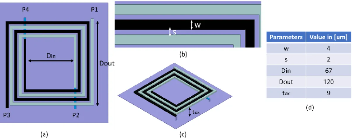
Figure 3-16 Designed interleaved transformer: (a) Top view (b) Top view (zoom) (c) side view (d) table with the values geometrical parameters.
M1 has been used as ground layer. The benefit of this choice is that having a metal ground in M1 reduce the losses of the substrate. The main disadvantage is that as the capacitors mentioned in the circuit model as Cox increase, it reduces the
self-resonance of the inductor (that directly affect the self-self-resonance of the coupler). The disadvantage by the way is negligible as the working frequency of the circuit is far from the self-resonance. Better results in terms of Q-factor could be
achieved if a Pattern Ground Shield (PGS) would have been used instead of a flat metal ground (it has been inserted in the list of the possible future works). This hybrid is based on an inductive coupling effect like conventional directional hybrids implemented using coupled lines. It consists of a pair of coupled transmission lines of electrical length equal to θ having characteristic impedances in the configuration even-and-odd respectively equal to Z0e and Z0o [20]. If the
impedances of the odd and even mode are designed satisfying 𝑍0 = √(𝑍0𝑒∙ 𝑍0𝑜)
then all the impedances of the device ports would be matched to Z0 at the design
frequency provided the electrical length is an odd multiple of a quarter of a wavelength.
Figure 3-17 Simulated transmission parameter and output phase deviation of the quadrature hybrid
The results of the S-Parameter plotted versus frequency in Figure 3-17 are obtained with a full wave simulation performed using a commercial finite element method solver for electromagnetic structures (HFSS, ANSYS). This plot show good results in terms of both transmission parameter and output phase difference
at central frequency and for a wide bandwidth. In particular, it can be noticed that the circuit has been designed to operate at the frequency of 24 GHz not in the classical “U-shape” but in the range where the direct and coupled ports have a positive and negative slope respectively (see the cross in the Figure 3-17). The main advantages of this approach are that it introduces less losses (only 0.39 dB) than the classical solution (sacrificing a bit the bandwidth) and in the same time we obtain an almost flat 90° output phase difference for an ultra-wide frequency range. In order to reduce the chip area occupied by the quadrature coupler, the layout topology was optimized by increasing the circuit density and by evaluating mutual coupling effects through a full-wave [21] simulation of the whole structure. The chip area occupied by the quadrature hybrid is equal to 120x120 μm2.
3.3.3 Phase delay line
As it is shown in the block diagram of Figure 3-8, three different phase delay blocks are required for the implementation of the 8x8 Butler matrix. In particular, 22.5°, 45° and 67.5° fixed delay lines need to be laid out in the circuit. In this work, phase delay lines were implemented using a transmission line π-model implemented through lumped elements.
Delay line Inductor [pH] Capacitor [fF] Size [um2]
22.5 ° 135 20.73 45
45° 230 50.5 50
67.5° 300 85 56
Table 3-2 Inductance and capacitance needed for phase delay
The π-network consists of two parallel capacitors and a series inductor. The inductor was designed using a rectangular geometry placed on the M6 level.
Figure 3-18 45° Delay line: (a) layout (b) Output phase.
Table 3-2 shows both inductance and capacitor values required to implement the circuit where it is shown also the overall size of each delay line. An example of the delay line model is shown in Figure 3-18a along with the simulated phase of the transmitted signal Figure 3-18b.
3.3.4 Crossover
Crossovers have been implemented taking advantage of the multilayer stack-up of the BiCMOS technology at hand. In particular, the two crossing lines were located on M6 and M4 metal layers while M1 layer also in this case act as a ground plane. The simulated isolation of the two crossing lines, shown in Figure 3-19, shows an isolation greater than 40 dB over the whole band.
Figure 3-19 Crossover isolation
3.3.5 Simulation results
The entire layout, with the exclusion of the measuring pads, is equal to 714 um x 650 um. As it can be observed in Figure 3-20 and Figure 3-21, the configuration proposed in this work shows an excellent input matching bandwidth for all ports. Indeed, the reflection coefficient remains below 20 dB in the whole simulation range. Furthermore, the insertion losses from the input to all the output ports remain within the 3 dB range for a 10% bandwidth.
Figure 3-20 Simulated input return loss of Butler matrix
Retu
rn
lo
ss
al
lp
or
ts
[d
B]
Figure 3-21 Simulated input insertion loss of Butler matrix
The output phases are in line with the ideal values and they were evaluated by analyzing the array factors obtained for different configurations of the Butler matrix. As it can be observed in Figure 3-23b, the simulated Butler matrix of Figure 3-22 generates 8 beams in the range from -60° to 60° as expected thanks to the output transmission phase shown in Figure 3-23(a).
Figure 3-23 Transmission Phase (a) Simulated radiation pattern using all input ports (b)
3.3.6 Measurement setup and final results
In order to measure the Butler matrix, a PCB test board was designed and prototyped. It is not so easy to design a test board for this small chip, which includes 16 RF ports. The configuration of the input and output ports is shown in Figure 3-24.
Figure 3-24 Submitted (left) and manufactured (right) layout of the 8x8 BiCMOS Butler matrix
As it can be observed, the input and output ports, located in position N-S in the chip, required a high-density arrangement which was necessary in order to
reduce the overall chip area. In order to bond this chip on the test board, shown in Figure 3-25, it was necessary to etch, within the PCB, a cavity in the way that the chip top surface was aligned to the PCB top layer. This solution was required to reduce as much as possible the length of the bonding length. As it can be observed in Figure 3-27, the bonding between the Butler matrix die and the PCB test board required a complex and highly dense net of transmission lines. The maximum length of the bonding path is equal to 700um while the distance between the die and the PCB microstrip line is equal to 100um.
Figure 3-25 PCB test board section.
Figure 3-26 Butler matrix integrated in a PCB board by wire bonding
Figure 3-27 Butler matrix integrated in a PCB board, zoom to the chip area and wire bonding
As can be clearly presumed from the Figure 3-26 and Figure 3-27, the integration of Butler's matrix on PCBs has been very intricate. The difficulty was in designing a board with cavities in order to reach the chip from the board with very short wire bonding. Wire bonding matching network has been realized with a short-circuited stub on the PCB side. Although de-embedding circuits for all the lines and connectors have been created (they are shown in Figure 3-28) the de-embedded procedure doesn’t include the eventual coupling between the wire bonding (that can be only predicted by EM simulation). It has been designed de-embedding circuit for the connector and for each branch of the BM and Hybrid Coupler.
Due to the variations of the production process and a minimum mutual coupling between the wire bonding, the output phases of the measured Butler matrix, even if respecting the frequency linearity, during phase de-embedding has been compensated adding a phase offsets to some output branches.
Figure 3-28 PCB designed test boards of Butler Matrix and Hybrid Coupler. It has been designed de-embedding circuit for the connector and for each branch of the BM and Hybrid
Coupler
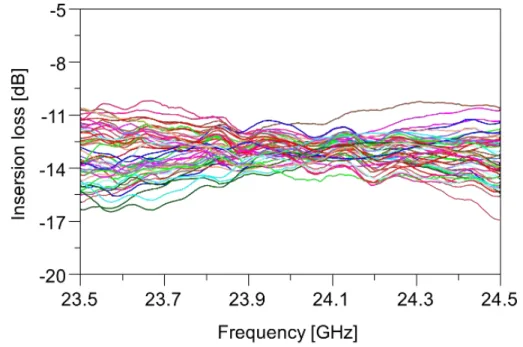
Figure 3-29 De-embedded measurement of Insertion Loss from all input ports trough all output of the Butler matrix
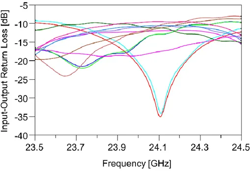
Figure 3-30 De-embedded measurement of input and output return loss of the Butler Matrix.
Due to the very long wire bonding and transmission line of the test board, the measured bandwidth of the Butler Matrix is very narrow. As it can be visible in Figure 3-29 and Figure 3-30 Insertion Loss and Return Loss show acceptable performances in terms of amplitude but in a very narrow bandwidth [from 23.5GHz to 24.5GHz] (4% of bandwidth).
Figure 3-31 De-Embedded measurement of output phase distribution of the Butler matrix fed though different input ports
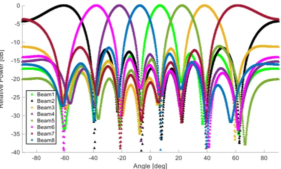
Figure 3-32 Simulated 24 GHz array factor based on the de-embedded measurement of the Butler matrix with isotropic antenna elements
The measured output phase distributions of the BiCMOS Butler matrix fed through different input ports is shown in Figure 3-31.
The measured S-parameters of the 8x8 Butler matrix are used to calculate the array factor of the linear antenna array [22]. Assuming ideal isotropic antennas with 𝜆/4 inter-element spacing, the calculated array factors of the 8 beams are plotted in Figure 3-32.
3.3.7
Post measurements studies and future worksAlthough the Butler matrix measurements were satisfactory in terms of amplitude and phase response, the operating bandwidth was much narrow than the simulated one. Some hypothesis has been discussed in the previous paragraph. The main bandwidth limiting factor is clearly related to the wire bonds which have been compensated through a single frequency optimization process. The following studies have been performed and they are still in the assessment stage:
1) The variance in the length of the wire bonding. In fact, the manufactured wire bonding results in 20% - 30% longer than the desired making useless (or less preforming) the matching network realized on the test board to compensate the inductance caused by the wire bonding.
2) The coupling between wire bonding. Similar to the problem of the point 1). Even if EM simulation of the wire bonding and the chip integration have been performed, having longer wire bonding cause more coupling between them.
3) Side coupling between close lines on the board side. Due to the high density of the circuit close to the chip, the isolation between the line is poor as we design a test board with 50um of isolation between the microstrip in this area. Also in this case, the coupling can be predicted but couldn’t be de-embedded.
Figure 3-33 Post measurements study on the test board: ADS representation of part of the board including coupling effect of wire bonding and microstrip
Possible solutions and future works are:
1) Flip chip integration: the main advantage to use this solution is that wire bonding are not needed anymore (main cause of phase offset and mismatching).
2) Multi-layer test board can be designed also to reduce the coupling effect between line. Closed lines can be drawn in different layers ensuring a good isolation.
3) Instead of solderless connectors on the side of the test board, it can be interesting to think about SMD connectors in order to reduce the size of the test board and also reduce the electrical length between the lines. See Figure 3-34 the proposed solution.
Wilkinson power divider
In microwave systems, the Wilkinson power divider is a component belonging to the family of power splitters that isolates the output ports from the other while maintaining the impedance matching to all ports. This circuit can be used to combine two signals because it consists of passive components and is therefore reciprocal. Published by Ernest J. Wilkinson in 1960 [23], this circuit finds its place in radiofrequency in multichannel systems because it is very effective in minimizing crosstalk.
At the base of the analog phased array system shown in Figure 3-35 there is the combining of the signal at the output of the phase shifter. As an example, a chip for SAT-COM on the move applications is reported on Fig. 3-35 and it shows how the signal should be combined (in RX case or split in TX case).
Figure 3-35 RX chip of a SAT-COM on the move application
Usually, when it is used as divider, the output power from ports 2 and 3 is equal to half of the incoming power, although an arbitrary power division may be
realized. It is possible to realize a multi-stage Wilkinson combiner in order to combine/split the signal in more than two parts. A Wilkinson power divider/combiner most of the time is realized with only passive component and for this reason is a reciprocal component, it means that the same circuit can be used as a divider or as a combiner. For this reason, to simplify, most of the time the term Wilkinson power divider (WPD in the follow) is used to define the reciprocal component.
Figure 3-36 General Wilkinson combiner
Wilkinson power divider state of art
As literature shows, there are several topologies and methodologies to realize a WPD. Herewith are reported some on chip CMOS and BiCMOS designs that can be found in the state of art.
In [24] an integrated equal-split WPD tailored for operation in the X-band is reported. The combiner features differential input/output ports with different characteristic impedances, thus embedding an impedance transformation feature. Over the frequency range from 8 to 14 GHz it shows insertion loss of 1.4dB, return loss greater than 12 dB and isolation greater than 10 dB. The circuit
is implemented in a SiGe bipolar technology, and it occupies an area of 0.12 𝑚𝑚2.
The schematic and a microphotograph of the proposed differential WPD is represented in Figure 3-37.
Figure 3-37 Schematic of the lumped-element equivalent circuit of the line section (left) and Microphotograph (right) of the WPD presented in [24]
In [25] a 24 GHz four-way miniature WPDs in a standard CMOS technology is presented. The chip area is significantly reduced using a lumped-element design, and the effective areas of four-way WPD are 0.11 𝑚𝑚2. The four-way WPD results
in an insertion loss 2.4 dB, an input/output return loss better 15.5 dB, and a port-to-port isolation 24.7 dB from 22 to 26 GHz. In Figure 3-38, the first demonstration of 24 GHz four-way WPD in a standard CMOS technology is shown.
Figure 3-38 Schematic (left) and Microphotograph (right) of the four way WPD presented in [25]
In [26] an ultra-compact WPD incorporating synthetic transmission lines at K-band in CMOS technology is presented. An improvement on the size reduction can be achieved by increasing the slow-wave factor of synthetic transmission line.
The presented WPD design is analyzed and fabricated by using standard 0.18 𝜇𝑚 IP6M CMOS technology. The prototype has a chip size of 480x90 𝜇𝑚2,
corresponding to 0.0002 𝜆2 at 21.5 GHz. The measured insertion loss and return
loss are approximately 4 dB and 17.5 dB from 16 GHz to 27 GHz, respectively. In Figure 3-39 a microphotograph of the proposed WPD is depicted.
Figure 3-39 The prototypes of the proposed CMOS WPD using synthetic transmission lines
Design of a multi Stage WPC/D
The goal of this project is to realize a compact multi-stage WPD with a minimum of 20 dB of isolation between the output ports and good performance in terms of phase and magnitude unbalance (typical requirements of an analog phase array system).
Goal Unit
BW 19 - 20 29 - 30 GHz
Insertion Loss <7.5 <7.5 dB
Input Return Loss <7.5 >14 dB
Output Return Loss >14 >14 dB
Phase Unbalance < 3 <3 deg
Amplitude Unbalance < 0.3 <0.3 dB Insertion Loss Flatness <0.2 <0.2 dBpp
Isolation >20 >20 dB
Although their design principle has a generic validity, in this project two multi-stage Wilkinson combiners has been designed for SAT-COM on the move applications. Therefore, the required working frequencies are 20-21 GHz for the downlink (Rx) and 29-30 GHz for the uplink (Tx). The full target set is reported in Table 3-3.
3.6.1 Schematic
The design flow starts with the studying of a distributed element WPD as reported in Figure 3-40. The next step has been to transform it in a lumped element WPD, as it illustrated in the Figure 3-41 with the corresponding formulas.
Figure 3-40 Distributed element Wilkinson combiner/divider
L = √2(𝑍₁∗𝑍₂)
2𝜋𝑓
C = 1
2𝜋𝑓√2(𝑍₁∗𝑍₂)
R = 2𝑍₀
Figure 3-41 Distributed element WPD
The same procedure was used to design both Rx and Tx combiner/dividers. The value obtained at 20 GHz and 30 GHz are reported in the Table 3-4.
@20 GHz @30 GHz
L [pH] 561 375
C [fF] 113 75
R [Ω] 100 100
Table 3-4 Lumped element values of a WPD designed at 20GHz and 30 GHZ
Figure 3-42 shown the return loss of both Rx and Tx single stage WPD.
Both circuits are implemented following the design flow. For this reason only the description of the Tx design will be reported in the following.
Figure 3-42 Return loss of 20 GHz (red line) and 30 GHz (blue line) WPD
In order to obtain a 4 ways power divider, a multi stage WPD has been designed. Once the circuits of WPD (one 50Ω input and two 50Ω outputs) has been designed, the second stage will be exactly a copy of the first stage and the inputs of the second stage has been connected directly to the two outputs of the first stage.
3.6.2 Layout
The layout of the two multi-stage WPDs has been designed in SiGe BiCMOS 0.25um technology (IHP SG25H3).
SG25H3 technology is a BiCMOS technology with a gate length of 25nm. The fT
of this technology is 120GHz and the standard backend option offers 3 thin metal layers, two Top Metal layers (Top-Metal1 -2 μm thick metal layer and TopMetal2 -3 μm thick metal layer) and a MIM layer.
Figure 3-43 Schematic of 2 stages WPD
In the layout, inductors and interconnection lines are placed on the thicker TM2 metal layer while M1 act as ground. MIM capacitors and poly-resistors from the design kit has been used. The final layout has been full wave electromagnetic simulated in ANSYS HFSS. Some small tuning of the inductance and capacitance values has been performed in order to compensate the effect of the interconnection lines. The density of the circuit has been optimized to reduce to the minimum the occupied chip area taking always in account the minimum
distance between components to avoid any kind of coupling. The final layout is shown in Figure 3-45. The two outputs port has been rotated of 90° respect to the input to simplify future interconnections with other component (i.e. two different Tx channels). The overall chip size (both layouts almost occupy the same area) is 680x550 𝑢𝑚2 (230x430 𝑢𝑚2 without pads). RF pads with 100 𝜇𝑚 pitch are used
to measure the performance of the device (S-parameters).
Figure 3-44 Final layout of a 30GHz Wilkinson combiner/divider
3.6.3 Comparison of measurements and simulations
The measurement setup is shown in Figure 3-45. Since the circuit is symmetric, to simplify the measurement two output ports have been connected to a 50Ω load and GSG and GSGSG probes have been used to measure the input port and the remaining 2 output ports respectively. The de-embedding procedure used to remove from the measurements the RF-pads has been TRL (through, reflect and line). Comparison between simulation (blue lines) and measurement (red lines) results for both case Rx and Tx are shown in Figure 3-46 and Figure 3-47.
Figure 3-46 Simulation (blue) vs measurement (red) results of Tx Wilkinson combiner
The results show a good agreement between measurements and simulations. Furthermore, this layout presents a good compromise between reduction area
and output isolation. Phase and amplitude imbalance are limited to 1° of phase and 0.1dB of amplitude imbalance. Insertion loss is less than 2 dB (1.9 in Rx case and 1.5 in Tx case).
Figure 3-47 Simulation (blue) vs measurement (blue) results of Rx Wilkinson combiner
Table 3-5 presents a comparison between this work and the state of art. As it can be noticed, there is only another work in literature reporting a multi-stage Wilkinson power combiner/divider on chip that’s why other works of single stage WPD has been included in the table. Form Table 3-5 is possible to assert that this is a most compact multi-stage WPD with the best performances in term of
bandwidth, insertion loss and isolation. The performance of this multi-stage WPD (even size and IL) can be compared with the single stage WPDs present in literature.
Ref. [26] [24] [25] work (Rx) This work (Tx) This
Process 0.18 𝜇𝑚 CMOS BiCMOS 0.35 𝜇𝑚 0.13 𝜇𝑚 CMOS BiCMOS 0.25 𝜇𝑚 BiCMOS 0.25 𝜇𝑚
# Output 2 2 4 4 4 Frequency and BW 𝑓0= 21 𝐺𝐻𝑧51.2% 𝑓0= 11 𝐺𝐻𝑧 51.2% 𝑓0= 24 𝐺𝐻𝑧 16.7% 𝑓0= 20 𝐺𝐻𝑧 50% 𝑓0= 30 𝐺𝐻𝑧 51% I.L.* 1 dB 1.4 dB 2.4 dB 1.9 dB 1.5 dB R.L.* 25 dB 12 dB 15.5 dB 30 dB 28 dB Iso.* 15 dB 10 dB 24.7 dB 25 dB 19 dB Max mag. Imbalance 0.11 dB 0.5 dB N.A. 0.14 dB 0.1 dB Max phase difference 0.18° 1.5° N.A. 1.1° 1.8° Chip size 0.043 𝑚𝑚0.0002 𝜆2 0 2 0.12 𝑚𝑚 2 0.00016 𝜆20 0.11 𝑚𝑚2 0.0007 𝜆20 0.099 𝑚𝑚2 0.00044 𝜆02 0.086 𝑚𝑚2 0.00072 𝜆02
* Parameter extracted at 𝑓0. IL is considered without the nominal losses for power splitting.
Table 3-5 Comparison the major characteristics of the proposed Wilkinson power combiners and other works
With the exception of the insertion loss (Rx case), all the requirements set in Table 3-3 have been achieved. Most likely, this small discrepancy between simulation and measurement results in terms of insertion loss come from bad prediction of the substrate losses or metal sheet resistances (considering valid the de-embedding procedure).
Phase shifter
Phased array systems will play a crucial role in 5G networks. Through them it is possible to obtain radiation patterns where the direction of the main lobe can be electronically steered, acting appropriately on the phase of the signal sent to each element radiant of the array [27]. Phase shifters are one of the fundamental components of a phased antenna systems. Figure 4-1 shows the basic architecture of a typical beamforming Tx network where the phase shifter (dashed lines) are highlighted.
Figure 4-1 Beam Forming network TX architecture
Phase shifter classification
RF Phase Shifters are used to change the transmission phase angle of an input signal. The input signal is shifted in phase at the output based on the configuration of the phase shifter selected. The transfer function can be defined by the scattering matrix in the form indicated as the follow:
𝑆 = [ 0 𝐴(𝜔)𝑒
−𝑗𝜓(𝜔)

![Figure 3-6 Die photograph of the 4x4 CMOS Butler matrix presented in [15]](https://thumb-eu.123doks.com/thumbv2/123dokorg/2872619.9527/29.892.338.606.558.901/figure-die-photograph-x-cmos-butler-matrix-presented.webp)