Università degli Studi di Ferrara
DOTTORATO DI RICERCA IN
FISICA
CICLO XXVII
COORDINATORE Prof. Guidi Vincenzo
Relaxed germanium epilayers on porous
silicon buffers for low dislocation content Ge
on Si virtual substrates
Settore Scientifico Disciplinare FIS/01
Dottorando Tutori
Dott. Calabrese Gabriele Prof. Guidi Vincenzo
Prof. Vincenzi Donato
iii
Table of Contents
Title Page………..………. i
Table of Contents………...… iii
Publications……….…… vi
Abstract………... vii
List of Figures………...viii
List of Tables………..……….……. xii
1
Introduction………...
11.1 Motivation of the work
………..……….………... 11.2 Thesis Outline
………...…... 22
Germanium heteroepitaxy on bulk silicon
………..…….... 32.1 Introduction
……….………... 32.2 Ge on Si VSs for III-V solar cells on silicon
…….……….…... 42.3 Basics of Ge epitaxy
………..……….……... 52.3.1 Lattice constant, critical thickness and relaxation…..…... 5
2.3.2 Growth modes in epitaxial systems………. 8
2.3.3 Dislocations in Ge………..… 9
2.4 Main challenges in Ge epitaxy on Si
………..……… 122.5 Assessment of threading dislocation density
……….…………. 132.5.1 High Resolution X-Ray diffraction analysis (HR-XRD)……... 15
2.6 Low energy plasma enhanced chemical vapor deposition
(LEPECVD)
………17iv
3
Porous silicon buffer layers
……….
203.1 Introduction
……….... 203.2 Fabrication and characterization of porous silicon………...
213.2.1 Current-voltage characteristic
………....
213.2.2 Theory of electrochemical etching
……….
233.2.3 Electrochemistry of silicon
……….……....
253.2.4 Characterization of porous silicon layers
…………...…
263.3 Porous silicon buffers grown at Ferrara University…………...……...
273.3.1 Double tank etching cell
……….………..
273.4 Microscope analysis of grown porous buffers……….
314
Ge epitaxy on porous silicon buffer layers
……….. 364.1 Introduction………
364.2 The effect of pSi buffer porosity on the Ge crystalline quality...…
374.2.1 HR-XRD and SEM analysis
………..……….
374.2.2 Reciprocal space maps analysis
………...….
484.2.3 Surface roughness analysis
………...……
554.3 The effect of pSi buffer layer thickness on the Ge
crystalline quality………...
585
Annealing of Ge on porous silicon virtual substrates
…….……...….. 635.1 Introduction
……… 635.2 High-resolution X-ray diffraction analysis
……….…………...645.2.1 Grazing incidence diffraction (GID) analysis…….………...… 68
v
5.2.3 Reciprocal space map analysis………..… 76
5.3 TEM analysis
……….… 795.4 Twin content in Ge epilayers
………..… 855.5 Threading dislocation density assessment
……….. 885.6 Applicability of obtained results to the very low TDD regime…....……
926
Conclusions and further work
……….... 936.1 Conclusions
………936.2 Further work
……….. 94References
……….………...…… 97vi
Publications
This thesis is based on data presented in the following papers:
G. Calabrese, S. Baricordi, P. Bernardoni, D. De Salvador, M. Ferroni, V. Guidi, V. Morandi, D. Vincenzi, Enhanced Threading Dislocation Reduction In Germanium
Grown On Porous Silicon On Annealing Due To Porous Buffer Reconstruction,
submitted to Applied Physics Letters
G. Calabrese, S. Baricordi, P. Bernardoni, D. De Salvador, M. Ferroni, V. Guidi, V. Morandi, D. Vincenzi, Ge Growth On Porous Silicon: The Effect Of Buffer Porosity On
The Epilayer Crystalline Quality, Applied Physics Letters 105, 122104 (2014)
G. Calabrese, S. Baricordi, P. Bernardoni, S. Fin, V. Guidi, D. Vincenzi, Towards III-V
Solar Cells On Si: Improvement In The Crystalline Quality Of Ge-On-Si Virtual Substrates Through A Low Porosity Porous Silicon Buffer Layer And Annealing, AIP
Conf. Proc. 1616, 37 (2014).
Other papers I published as corresponding author not related to this thesis work:
G. Calabrese, F. Gualdi, S. Baricordi, P. Bernardoni, V. Guidi, L. Pozzetti, D. Vincenzi, Numerical Simulation Of The Temperature Distortions In Ingap/Gaas/Ge
Solar Cells Working Under High Concentrating Conditions Due To Voids Presence In The Solder Joint, Solar Energy 103 (2014) 1–11.
F. Aldegheri, S. Baricordi, P. Bernardoni, M. Brocato, G. Calabrese, V. Guidi, L. Mondardini, L. Pozzetti, M. Tonezzer, D. Vincenzi, Building Integrated Low
Concentration Solar System For A Self-Sustainable Mediterranean Villa: The Astonyshine House, Energy and Buildings 77 (2014) 355–363.
S. Baricordi, G. Calabrese, F. Gualdi, V. Guidi,M. Pasquini, L. Pozzetti, D. Vincenzi,
A Joint Thermal-Electrical Analysis Of Void Formation Effects In Concentrator Silicon Solar Cells Solder Layer, Solar Energy Materials and Solar Cells Volume 111 (2013)
vii
Abstract
While silicon represents the dominant material in the semiconductor industry, the continuous improvement in the performance of Si based devices is reaching its upper bound due to the approaching of insuperable physical limitations intrinsic to Si, which requires the introduction of new semiconductor materials and the development of new assembly techniques to guarantee the future performance improvement and reduction in fabrication costs. The integration of high-quality germanium epilayers on Si substrates has received great attention from the semiconductor community due to the chance to extend the range of performance offered by Si-based technology by taking advantage of both the superior properties of Ge such as a higher carrier mobility, a lattice constant close to that of GaAs which enables III-V epitaxy and a quasi-direct bandgap, and of the possibility of strain and bandgap engineering offered by the formation of a heterojunction.
To overcome the 4.2% lattice constant mismatch existing between Ge and Si which hamper the direct integration approach, this thesis investigates a novel technique for the realization of high-quality Ge on Si virtual substrates (VSs), consisting in the introduction of a porous silicon (pSi) buffer layer in between Ge and Si. pSi is a versatile, self-assembled, nanomaterial which can be realized at very high growth rates through electrochemical etching of Si. Thanks to its reduced Young’s and shear moduli pSi can deform during epitaxy, potentially alleviating part of the lattice mismatch between Ge and Si and reducing the density of misfit dislocations and associated threading segments necessary for complete Ge relaxation. Together with the very high throughput of the anodization process, other fundamental advantages of the proposed approach are its low cost, its simple scalability to large area Si substrates and the possibility to lift-off the grown epilayers from the starting substrates, giving Ge on pSi VSs the possibility to outperform other existing techniques for Ge integration on Si.
During the course of this work, several Ge on pSi VSs have been grown through low energy plasma enhanced chemical vapor deposition (LEPECVD) technique, and the resulting crystalline quality has been compared to that of Ge on Si VSs. Using X-ray diffraction techniques, together with electron microscopy analysis and selective etching techniques, it will be shown how the main physical parameters of pSi buffers affect the crystalline quality of Ge heteroepilayers. Finally, it will be demonstrated that strong threading dislocation reduction is possible in Ge grown on low porosity pSi buffers compared to Ge on bulk Si, at parity of experimental conditions, and the main mechanisms responsible for crystalline quality improvement in Ge grown on pSi will be uncovered.
viii
List of Figures
Figure 2.1: Fraunhofer ISE roadmap for the development of III-V multi-junction solar cells. Four different solar cell concepts employing a Ge bottom cell are shown, both lattice matched (a-c), metamorphic (d) and inverted metamorphic (e). After Ref [40]……….…. 5 Figure 2.2: a) Critical thickness of Si1-xGex layer as a function of Ge content and b) maximum critical
thickness of a Si1-xGex stable layer with and without Si cap layer. After Ref. [42]………... 7
Figure 2.3: Schematic representation of the different growth modes found in epitaxial processes. Adapted from Ref. [46]……….. 9 Figure 2.4: Schematic representation of the eight slip systems existing for 60° dislocations in Ge epitaxial layers grown on (001) Si. After Ref. [48]……….. 10 Figure 2.5: Lifetime of electrons and holes minority carriers as a function of TDD in GaAs epilayers grown on Ge on Si VSs. After Ref. [56]………... 13 Figure 2.6: (004) Ge RC for Ge grown on pSi and its best Gaussian approximation (in red). Deviations from the ideal Gaussian behavior are found in the tail regions as well as in the central region of the Ge diffraction peak………... 16 Figure 2.7: Schematic diagram of the LEPECVD system installed at Ferrara University……….... 18 Figure 3.1: Typical I-V curve for the electrochemical etching of moderately doped a): p-type Si and b): n-type Si. After Ref. [89]………. 23 Figure 3.2: Reaction mechanism for the electrochemical etching of Si in HF solution. Adapted after Ref. [99]……….… 25 Fig 3.3: Image of the double tank etching cell developed for the electrochemical etching of small area pSi buffers (left) and CAD drawing showing the cross-section of the realized double tank etching cell.28 Figure 3.4: 100 mm n-type Si wafer (001) oriented with resistivity of 2.5 mΩ cm showing different porous buffers on its surface. A magnified image of one porous layer reveals the presence of striations in the starting Si substrate……….. 30 Figure 3.5: Thickness and porosity of grown pSi layers as a function of provided current density for 20s anodization time of 3.9mΩcm p-type Si (001) oriented with 6° offcut towards [111]. Used electrolyte is a solution of HF and ethanol in the volume ratio (3:1)………....31 Figure 3.6: Low magnification (20K) cross-section SEM images of a) 22% pSi, b) 30% pSi, c) 40% pSi and d) 48% pSi………. 32 Figure 3.7: Magnified SEM image of a) 22% pSi and b) 48% pSi showing the pore morphology…….. 32 Figure 3.8: Bright field XTEM micrographs of as-grown pSi having porosity of 22%... 33 Figure 3.9 XTEM micrographs of annealed 22% pSi showing a region almost depleted of pores at pSi surface………... 34 Figure 3.10: a) low magnification STEM image of annealed 22% pSi showing a porosity gradient within the grown buffer and b) high magnification STEM image of the top part of annealed 22% pSi…….… 34 Figure 4.1: Different pSi buffers having porosity values of 22%, 30%, 40% and 48% grown on the same 100 mm Si wafer (001) oriented………. 39
ix
Figure 4.2: Omega/2Theta semi-log plot of the (004) diffraction peak of as-grown pSi samples... 41 Figure 4.3: a) – e) Omega/2Theta semi-log plot of the (004) diffraction peak of Ge grown on Si and on pSi. In Figure 4.3 b) the diffraction peak of annealed 22% pSi in case of no epitaxy has been superimposed to the collected Omega/2Theta scan. After epitaxy a single pSi peak at small diffracting angle is observed for all samples except Ge on 22% pSi, which shows two peaks arising from pSi at large diffracting angle indicating separation of pSi in two sublayers and contraction in the out-of-plane direction………. 44 Figure 4.4: a) and b) cross section SEM images of Ge grown on 22% and 48% porous buffers. c) and d): magnified SEM images of the Ge/pSi interfaces………..… 46 Figure 4.5: Cross-section SEM images of the Ge/22% pSi interface. The arrows indicate small voids in the bottom part of the Ge epilayer………. 47 Figure 4.6: Plan-view SEM images of sample surface after EPD analysis for Ge grown on a) bulk Si, b) 22% pSi, c) 30% pSi..………. 48 Figure 4.7: (004) and (224) RSMs iso-intensity contour plots of Ge grown on bulk SI and on different porosity pSi buffers. In the insets the magnified Si and pSi RELPs for Ge grown on 22% and 48% pSi are shown. A magnified image of the 30% and 40% pSi RELPs is not reported as the strain state of these buffers is very similar to that of 48% pSi………... 49 Figure 4.8: (004) RCs for Ge grown on bulk Si and on the different investigated buffers extracted from symmetrical RSMs. The reported FWHM are obtained from Gaussian fitting of the RC, which are shown in Figure………... 50 Figure 4.9: 5 µm x 5 µm AFM micrographs of Ge grown on bulk Si and on the different investigated pSi buffers………. 56 Figure 4.10: RMS roughness of as-grown Ge epitaxial layers on bulk Si and on the investigated porous buffers……….. 57 Figure 4.11: (004) Omega/2Theta scans collected in open detector diffraction mode for Ge epilayers grown on n-type pSi buffers anodized for different etching times. The HF:ethanol volume ratio is 7:1 and the current density is fixed at 45 mAcm-2……….… 60
Figure 4.12: Cross section SEM image of 750 nm-thick Ge epilayer grown on a 600 nm-thick n-type pSi. pSi buffer porosity is 26%. 3D island growth is visible at Ge surface……….… 62 Figure 5.1: Evolution of the Ge FWHM collected in GID configuration for both 0° and 180° azimuth angles as a function of annealing temperature………..… .65 Figure 5.2: (224) RSMs of Ge grown on 22% pSi around the pSi and bulk Si reciprocal lattice points collected at a) 26°C, b) 180°C, c) 340°C and d) 500°C, respectively……… 66 Figure 5.3: (224) RSMs of Ge grown on 30% pSi around the pSi and bulk Si reciprocal lattice points collected at a) 26°C, b) 180°C, c) 340°C and d) 500°C, respectively………. 67 Figure 5.4: Omega/2Theta scans collected in GID configuration for Ge grown on bulk Si (grey line) and on 22% pSi (black line) during N2 annealing at the temperature of a) 26°C, b) 180°C, c) 340°C
and d)
500°C………. 69 Figure 5.5: (224) Omega/2Theta scans for Ge grown on bulk Si (grey line) and on 22% pSi (black line) in GID configuration after 3 cycles of H2 annealing at 750°C………... 70
x
Figure 5.6. (224) GID Omega/2Theta scans during heating up (top curves) and cooling down (bottom curves) the substrate for a) Ge grown on bulk Si and b) Ge grown on 22% pSi………..…. 71 Figure 5.7: FWHM of the Ge epilayers retrieved from HT-XRD (224) Omega/2Theta scans in GID configuration as a function of annealing temperature. The FWHM measured after 3 cycles of H2
annealing at 750°C is also reported……….. 72 Figure 5.8: Omega/2Theta scans collected in GED configuration for Ge grown on bulk Si (grey line) and on 22% pSi (black line) during N2 annealing at the temperature of a) 26°C, b) 180°C, c) 340°C
and d) 500°C……….…… 74 Figure 5.9:.(224) Omega/2Theta scans for Ge grown on bulk Si (gray line) and on 22% pSi (black line) in GED configuration after 3 cycles of H2 annealing at 750°C………... 75
Figure 5.10: FWHM of the Ge epilayer retrieved from HT-XRD (224) Omega/2Theta scans in GED configuration as a function of annealing temperature. The FWHM measured after 3 cycles of H2
annealing at 750°C is also reported in Figure. The data for both Ge grown on bulk Si and on 22% and 30% pSi are shown……….. 75 Figure 5.11: (004) symmetrical RSMs after three cycles of H2 annealing at 750°C for: a) Ge grown on
bulk Si and b) Ge grown on 22% pSi. A smaller spreading of the Ge reciprocal lattice point is observed in both QY and QX direction for Ge grown on 22% pSi, together with a smaller net average
crystallographic tilt of the Ge epilayer with respect to the Si substrate………...… 77 Figure 5.12: (224) RSMs after three cycles of H2 annealing at 750°C for Ge grown on 22% pSi…….. 78
Figure 5.13: Low manification XTEM image of Ge grown on bulk Si collected in two-beam condition.80 Figure 5.14: XTEM micrographs collected at a) low mangification and b) high magnification of Ge grown on bulk Si showing a high TDD within Ge and a confined dislocation network at the interface..80 Figure 5.15: Low magnification XTEM micrograph of Ge grown on 22% pSi after 30 minutes H2
annealing at 750°C. Extended defects are mainly confined in the first µm of the Ge epilayer………... 81 Figure 5.16: XTEM images of the Ge/pSi heterointerface after 30 minutes H2 annealing at 750°C
collected at a) low magnification and b) high magnification………. 82 Figure 5.17: XTEM micrograph of the Ge/22% pSi interface after 30 minutes H2 annealing at 750°C.
TDs propagating parallel to the growth interface are visible……….… 83 Figure 5.18: High magnification XTEM micrograph of the Ge/22%pSi heterointerface showing pinned MDs at the growth interface. Red squares indicate MDs while orange rectangles indicate amorphous regions in pSi in correspondence of each MD. In beetween two distinct MDs pSi exhibits a well ordered pattern in the green rectangles, indicating a monocrystalline structure at the growth interface far from MDs. A selected area diffraction pattern shows crystalline Ge is grown on top of pSi with the same crystallographic orientation………. 85 Figure 5.19: a) Magnified XTEM image showing twinned planes in Ge grown on bulk Si and b) the corresponding selected area diffraction pattern……….. 86 Figure 5.20: Ge (111) pole Figure for a) Ge grown on bulk Si and b) Ge grown on 22% pSi…………. 87 Figure 5.21. Double-crystal (004) RCs for Ge grown on bulk Si (gray line) and on pSi (black line) collected after three cycles of H2 annealing at 750°C……… 89
Figure 5.22: plan view TEM images of annealed Ge grown on bulk Si (top) and Ge grown on 22% pSi (bottom). TDD is almost reduced by one order of magnitude in presence of pSi………. 90
xi
Figure 5.23: Simulation and experimental data of TDD at Ge surface for as-grown or single annealed Ge on Si (filled squares) or after cyclic annealing (open square and filled triangles). The TDD obtained in this work is also reported for comparison. Adapted from Ref [146]………. 91 Figure 6.1: Proposed approach for the growth of III-V solar cells on silicon substrate and successive lift-off using a pSi double layer……….. 96
xii
List of Tables
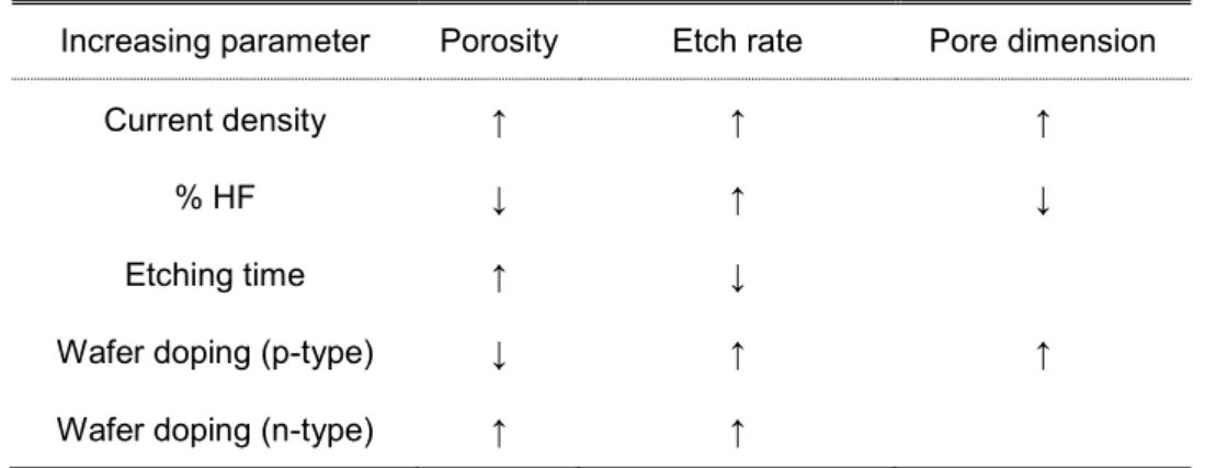
Table 3.1: The effect of the main electrochemical etching parameters affecting pSi formation………. 24
Table 4.1: Growth parameters of electrochemical etched pSi samples (p-type, nominal resistivity 2-20 mΩ cm) and their physical parameters determined by gravimetric measurements………..…… 40
Table 4.2: Physical parameters of grown pSi buffers……….... 41
Table 4.3: Lattice misfit for Ge grown on bulk Si and on the different grown pSi buffers……… 53
Table 4.4: Ge fraction in the epitaxial layer for different buffer porosity………... 54
Table 4.5: Physical parameters of grown Ge epilayers……….…… 55
Table 4.6: Ge FWHM and pSi lattice mismatch for different anodization times of 3.6 mΩ cm oriented n+ Si anodized in the dark. All buffers are grown at a constant current density of 45 mAcm-2 and using a HF:ethanol volume ratio of 7:1………..………. 61
Chapter 1
Introduction
1.1 Motivation of the work
Although silicon has enabled the growth of the semiconductor electronic industry, it was not the first investigated material for this kind of application. The first transistor was realized in 1947 using germanium bulk crystal as a raw material, and the germanium diode and bipolar-junction-transistor technology largely dominated the initial years of the solid-state industry [1,2]. Only the discovery of SiO2 dielectric passivation and the metal-oxide-semiconductor-field-effect-transistor (MOSFET) process in the mid-1960s made silicon to become the dominant semiconductor in industry [1]. Today silicon based semiconductor devices account for over 97% of all the microelectronic devices [3] which represent the large portion of the several hundred billion dollars semiconductor industry. Silicon represents the ideal semiconductor from a fabrication point of view, but it is hardly the best available material from a device perspective. Both the electron and hole mobility in Si are smaller than that of Ge and III-V semiconductors, which can take advantage of improved device performance and reduced power consumption, while the indirect bandgap of Si limits its application in optoelectronic devices. Among all known semiconductor materials, germanium offers the highest hole mobility, making it the most promising material for p-type MOSFETs (PMOSs) capable to outperform the current strained silicon PMOSs [1]. Apart from high mobility applications, Ge can take advantage of a lattice constant close to that of GaAs, thus enabling the epitaxy of III-V semiconductors, and of a quasi-direct bandgap, suggesting the possibility of light emission and detection in Ge by employing strain and bandgap engineering [4,5]. To be fully compatible with the current complementary metal-oxide-semiconductor (CMOS) manufacturing process, the integration of germanium based devices on silicon substrates is of foremost importance, so that the strong increase in manufacturing cost that would arise from the use of non –silicon substrates can be avoided [1].
The direct integration of Ge on silicon substrates is hampered by the 4.2% lattice mismatch existing between Ge and Si, leading to the nucleation of a high density of dislocations, which increases device dark current and introduces non-radiative
2
recombination centers degrading device performance. To overcome this issue, Si substrate pattern techniques have been recently developed, taking advantage of confinement and expulsion of generated threading dislocations (TDs) which can glide at the edges of grown mesas [6,7] and towers [8,9] and annihilate, resulting in excellent Ge crystal perfection. However, geometrical considerations cause these techniques to effectively reduce the dislocation density when the growth region is small enough (typically < 40 µm [5]), making the reduced area of the high-quality Ge crystals, together with the use of typically time-consuming and costly substrate pattern techniques, the main limitation of these approaches.
A maskless substrate pattern technique which can potentially reduce to the device grade the dislocation density in large area Ge epilayers on Si, while taking advantage of very high throughputs and low fabrication costs, consists in the introduction of a porous silicon (pSi) buffer layer in between the Si substrate and the Ge epilayer. If the compliant structure of pSi could be finely tuned to accommodate a large portion of the lattice mismatch existing between Ge and Si, pSi would likely represent the ideal buffer for Ge integration on silicon, for the realization of Ge based devices or for the growth of III-V semiconductors on Si.
1.2 Thesis outline
This thesis is devoted to the investigation of mesoporous silicon as a buffer layer for the growth of high-quality Ge epilayers integrated on silicon substrate with reduced dislocation content compared to Ge directly grown on bulk Si. In Chapter 2 will be discussed the main challenges in Ge epitaxy on Si and will be presented a description of the low energy plasma enhanced chemical vapor deposition (LEPECVD) tool used for epitaxial growth. In Chapter 3 it will be investigated the formation mechanism of pSi buffers, their growth using a double tank etching cell developed during the course of this thesis and their characterization. In Chapter 4 the epitaxial growth of Ge on the realized porous buffers will be investigated and compared with the direct integration of Ge on bulk Si. In chapter 5 will be discussed the effect of high temperature annealing on the crystalline quality of grown Ge on Si VSs, and the main mechanisms for crystalline quality improvement in Ge grown on pSi buffers will be revealed. Finally, the main conclusions of this thesis will be summarized in chapter 6, together with some suggestions on how to improve the obtained results in future investigations starting from the data presented in this work.
3
Chapter 2
Germanium heteroepitaxy on bulk silicon
2.1 Introduction
In the past decades, Ge on Si virtual substrates (VSs) have been extensively investigated due to a wealth of applications in a wide range of high-performance optoelectronic and microelectronic devices and their compatibility with silicon CMOS technology. The first successful approach to grow high-quality Ge epilayers on Si substrate is dated 1984, when Luryi and collaborators employed a graded SiGe buffer layer to reduce the dislocation content within the Ge upper layer [10]. Graded SiGe buffers have been successively investigated by Fitzgerald and collaborators, which demonstrated a strong reduction in the nucleation of dislocations by employing a low grading rate of ~10%/µm and ex-situ chemical mechanical polishing to reduce both the surface roughness introduced by cross-hatch pattern and dislocation pile-up that hinders dislocation gliding requiring the nucleation of additional defects [11]. Good crystalline quality Ge epitaxial layers on Si have also been obtained by direct Ge epitaxy without the introduction of SiGe buffers, which main disadvantage consist in increasing the total thickness of the device, increasing its thermal resistance and the fabrication cost. Different groups investigated direct Ge epitaxy on Si using chemical vapor deposition (CVD) through a double-step epitaxial process: according to this approach a thin Ge seed layer is initially grown on Si at the low temperature of 320-360°C resulting in an almost flat epitaxial layer, as islanding is effectively suppressed by the low Ge surface diffusivity at low temperature. Afterwards, a homoepitaxial Ge layer is grown at higher temperature (˃ 600°C) on the grown Ge seed in order to increase the growth rate [12, 13]. Other investigated techniques for the realization of high-quality Ge epilayers on Si involve ion implantation followed by high temperature annealing [14, 15], surfactant-mediated epitaxy [16] and substrate pattern techniques such as shallow trench isolation [6,7] and growth on pillars [8,9].
With the continuous improvement in the crystalline quality of Ge heteroepilayers on Si, Ge on Si VSs have been used in the realization of high mobility p-MOS devices [17, 18], near-infrared photodetectors [19-21], Light Emitting Diodes (LEDs) [22-24] electrically
4
pumped lasers [25-26], and modulators [27]. Apart from Ge based devices, great interest towards Ge on Si VSs arise from the possibility to integrate III-V semiconductors or GeSn alloys on Si, making these substrates the ideal platform for high-efficiency multijunction solar cells [28-31], high-performance Ge/III-V MOS devices [32,33] and group IV direct-bandgap semiconductors useful for optoelectronic applications [34-36]. Even though in the last years layer transfer technique combined with semiconductor wafer bonding has led to excellent crystalline quality of bonded III-V layers on silicon characterized by low dislocation density [37] the direct epitaxy approach to integrate Ge and III-V semiconductors on Si still remains very attractive due to its relative simplicity and the possibility to reduce fabrication costs.
Recently, plasma enhanced chemical vapor deposition (PECVD) has been developed to allow high-quality Ge epilayers on Si at high growth rate and reduced thermal budget thus positioning this technique in advantage with respect to standard techniques such as chemical vapor deposition (CVD) and molecular beam epitaxy (MBE) [38].
Even though low values of threading dislocation density (TDD) suitable for subsequent epitaxial growth have been demonstrated using different techniques, there is still the lack for a low-cost, high-throughput technique easy scalable to large wafers size able to provide high-quality Ge on Si VSs to the optoelectronic and microelectronic industry.
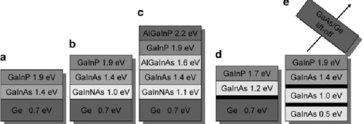
2.2 Ge on Si VSs for III-V solar cells on silicon
One of the main applications of high-quality, relaxed, Ge epilayers on Si is the possibility to integrate III-V semiconductors on a low-cost, large availability, high thermal dissipation and light substrate for the realization of very-high efficiency and low-cost III-V solar cells on Si. Most multijunction solar cells, both for terrestrial and space applications, typically employs a Ge bottom cell to convert the infrared portion of the solar spectrum on top of which III-V semiconductors are epitaxially grown. As an example, the III-V multi junction solar cell concepts under investigation at Fraunhofer ISE are shown in Figure 2.1. Lattice matched triple-junction and quadruple-junction solar cells (a-c) employing a Ge bottom cell are under investigation, as well as lattice mismatched metamorphic devices (d) and inverted metamorphic (e) grown on Ge [39]. The use of a Ge substrate provides lattice matching with the upper subcells and mechanical stability to the device during fabrication steps, but is unnecessary from an electrical point of view and contribute in large part to the final cost and weight of the device. 5 µm of Ge absorb 85% of the GaAs-filtered sunlight compared to the absorption of a thick Ge wafer [40], which thickness is typically in the rage 130-180 µm. As a consequence a thickness comprised between only 2 and 5
5
µm is necessary for the Ge sub-cell in a multi-junction device in order to ensure current matching with other sub-cells [41]. For space applications, the Ge substrate is typically removed from the solar cell at the end of the growth process with a selective chemical etching or with a wafer cutting. This reduces the weight of the device but the expensive Ge substrate is lost during the cutting process. For terrestrial applications the situation is more critical as final cost of the PV device is of paramount importance in determining the success of the technology, so that the use of thick and electrically inactive Ge substrate is of particular disadvantage. The epitaxial integration of III-V solar cells on silicon substrate could lead to a great advantage in terms of final device cost, weight, mechanical resistance, thermal conductivity, availability and wafer size. High-quality, smooth and relaxed Ge on Si virtual substrates with low dislocation content represents hence the ideal platform for the successive epitaxy of III-V semiconductors for very high-efficiency multi-junction solar cells thanks to the possibility of a net cost saving as high as 75% by switching from small area 100-150 mm Ge wafers to Ge virtual substrates grown on cheaper Si wafers having a larger area up to 300 mm [40].
Figure 2.1: Fraunhofer ISE roadmap for the development of III-V multi-junction solar cells. Four different solar cell concepts employing a Ge bottom cell are shown, both lattice matched (a-c), metamorphic (d) and inverted metamorphic (e). After Ref [40].
2.3 Basics of Ge and SiGe epitaxy
2.3.1 Lattice constant, critical thickness and relaxation
The epitaxial growth of high-quality lattice mismatched epitaxial layers represents one of the most investigated and challenging researches in the field of semiconductors. In particular the heteroepitaxal growth of Ge on Si has been deeply investigated for more than 30 years because of the large number of high-performance and cost-effective
6
potential applications it offers. Ge and Si are both group IV materials with face centered cubic (fcc) diamond-like lattice structure. Si and Ge lattice constants are 𝑎Si= 5.4307 Å and 𝑎Ge= 5.6580 Å respectively, and their lattice constant mismatch is 4.18%. This value
represents a very large lattice mismatch for epitaxial systems, causing the introduction of a high density of defects In the epitaxial layer when pure Ge is grown directly on bulk Si above the critical thickness (hc). Si1-xGex alloys of any concentration x can be grown, which lattice constant 𝑎Si1−xGex is given by a small parabolic deviation of the Vegard's rule, which states that there is a linear relation between the lattice parameter of a solid solution alloy and the concentrations of the constituent elements.
The relative variation in lattice constant 𝜀 of a Si1-xGex alloy is given by [42]:
𝜀 =𝑎Si1−xGex− 𝑎Si
𝑎Si = 0.00501𝑥2+ 0.03675 x 2.1
It follows that, in order to accommodate the lattice mismatch, a Si1-xGex layer grown on a Si substrate results under compressive stress. This mismatch can also be accommodated by the introduction of dislocations at the epilayer/substrate interface to partially or totally relieve the accumulated stress, when the thickness of the layer exceeds hc.
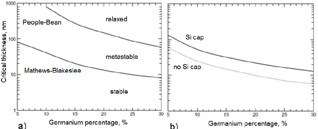
During heteroepitaxy, if the thickness of the epitaxial layer does not exceed hc, no dislocations are created at the growing interface and within the epitaxial layer and only elastic deformation occurs. In this case the epilayer is described as pseudomorphic. In particular cases the thickness of the epilayer can also exceed hc without nucleation of dislocations. As an example when low thermal budgets are employed during film growth, dislocation formation can result energetically unfavorable. Such film is described as metastable and subsequent thermal treatment will cause the film relaxation through the formation of dislocations at the interface. The critical layer thickness strongly depend on the lattice constant mismatch between the epilayer and substrate and hence on the Ge content when SiGe in grown on Si. for pure Ge on bulk Si hc is comprised between 1 and 2 nm [43], making this small thickness practically not useful for device applications. On the other hand, for Ge concentrations lower than 25% more than 10 nm can be grown without dislocation formation. Matthews and Blakeslee studied the critical layer thickness related to the mechanical equilibrium of an existing threading dislocation [44], obtaining the maximum layer thickness for stable layers. Also People and Bean investigated the critical layer thickness of an epitaxial system assuming that the generation of misfit dislocations to be determined solely by energy balance and they obtained the maximum thickness for metastable epilayers [45]. The critical layer thickness for a SiGe alloy grown on Si as a function of Ge percentage obtained with the different approaches of Matthews
7
and Blakeslee and People and Bean is shown in Figure 2.2 a), after Ref. [42]. Apart from the lattice mismatch, additional factors may influence the critical layer thickness such as the eventual the presence of a Si cap layer, which for example can double the value of hc. (see Figure 2.2 b)).
Figure 2.2: a) Critical thickness of Si1-xGex layer as a function of Ge content and b) maximum
critical thickness of a Si1-xGex stable layer with and without Si cap layer. After Ref. [42].
A pseudomorphic dislocation free SiGe layer grown on a (001) Si substrate has a tetragonally distorted unit cell with in-plane lattice constant:
𝑎𝑆𝑖𝐺𝑒|| = 𝑎𝑆𝑖 2.2 and out-of-plane lattice constant:
𝑎𝑆𝑖𝐺𝑒⊥ = 𝑎𝑆𝑖(1 + 𝑘𝜀) 2.3
where 𝑘 is an adimensional coefficient which takes into account the material stiffnes and for SiGe is:
𝑘 = 1 +2𝐶12
𝐶11 ≈ 1.75 2.4
𝐶12and 𝐶11 are the elastic stiffness constants relating the fraction change in length (εxx for
C11 and εyy , εzz for C12) to the stress components.
For any Ge concentration the degree of relaxation is defined as:
𝑅 =𝑎𝑆𝑖𝐺𝑒||− 𝑎𝑆𝑖
8
where 𝑎𝑆𝑖𝐺𝑒|| is the in-plane lattice constant of the epilayer and 𝑎0 is the relaxed epilayer lattice constant. For a pseudomorphic layer R=0 while in general 0 ≤ 𝑅 ≤ 1. As for partially relaxed epilayers the lattice constants depend on the Ge content and the degree of relaxation, in this case both lattice constants must be measured to obtain Ge content and R. Directly measuring the in-plane lattice constant, for example through high-resolution x-ray diffraction reciprocal space maps, has the advantage that no assumption has to be made on Ge or SiGe elastic constants, thus resulting in a more accurate measure.
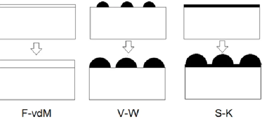
2.3.2 Growth modes in epitaxial systems
In general three different growth modes exist for heteroepitaxial processes: the Frank-van der Merwe (F-vdM) or two dimensional layer by layer growth mode, the Volmer-Weber (V-W) or three dimensional island growth mode and the Stranski-Krastanov (S-K) growth mode, given by a combination of the former modes (Figure 2.3). Which growth mode occurs depends on the free-energy balance between the surfaces and the interface involved in the reaction and is determined by the simple following equation [46]:
𝛾𝐿𝑆+ 𝜎𝐿≤ 𝜎𝑆 (2.6)
where 𝛾𝐿𝑆 represents the sum of the interface energy, 𝜎𝐿 the surface energy of the epilayer and 𝜎𝑆 the surface energy of the substrate. The F-vdM growth mode occurs when disequation (2.6) is satisfied: this is the case of homoepitaxial processes where 𝛾𝐿𝑆 = 0 and 𝜎𝑆= 𝜎𝐿 as not lattice mismatch exist between the substrate and the growing epilayer. In F-vdM growth mode the growing layer wets the surface of the substrate completely. On the other hand V-W growth mode occurs when disequation (2.2) isn’t satisfied from the beginning of the epitaxial deposition.
If at the start of the growth disequation (2.6) is satisfied and becomes unsatisfied as the epitaxial growth continues, i.e. if the balance of the existing forces results modified during epitaxy, S-K growth mode proceeds. This occurs when the growing epilayer and the substrate have a relatively large lattice mismatch, which cause the accumulation of the large strain in the epilayer during the initial stage of epitaxy. This is the case of Ge epitaxy on Si, where the first few monolayers of Ge are grown under compressive strain in a layer by layer mode, up to hc. For larger thicknesses the accumulated strain is relaxed by the introduction of dislocations and the Ge growth proceeds by islands as the growing layer tries to minimize both its surface and interface energy.
9
Figure 2.3: Schematic representation of the different growth modes found in epitaxial processes. Adapted from Ref. [46].
2.3.3 Dislocations in Ge
When Ge is grown on Si above hc, misfit dislocations (MD) are nucleated at the epilayer/substrate interface to relieve the strain accumulated in the epitaxial layer, which relax plastically. MDs do not degrade the crystalline quality of the active Ge epilayer since these are confined at the growing interface. However, their nucleation is always associated with the formation threading dislocation (TD) segments within the epitaxial layer, which introduce non-radiative recombination centers in the active layers degrading carrier lifetime and increasing the device dark current. In the core of a dislocation dangling bonds and large local strains are present, while near the core the inter-atomic bonds are only weakly distorted [47]. Each dislocation is characterized by a dislocation line and a Burgers vector b, which defines the magnitude and the direction of the crystal lattice distortion introduced by the dislocation. TDs, which do not relax the lattice constant mismatch, can’t end inside the crystal and thread within the epilayer until they encounter a free interface such as a semiconductor/air or semiconductor/oxide interface. Usually, dislocations thread within grown epilayers and terminate at the top epilayer surface, which is typically the nearest interface to the growth interface. Otherwise dislocations can form a closed loop or branch into other existing dislocations [47] and TDs that meet at a point with opposite Burgers vector annihilate. When three or more dislocations meet at a point, these form a node, and Burgers vector must conserve.
Two main kinds of dislocations exist depending on the mutual orientation of the dislocation line and the Burgers vector. Edge dislocations are line defects with perpendicular dislocation line and Burgers vector, while screw dislocations present parallel dislocation line and Burgers vector. In Ge and SiGe typically dislocations are of
10
mixed character (i.e. an arbitrary angle exists between dislocation line and Burgers vector) and pure edge and screw dislocations are rarely observed. In particular, 60° MDs which have a 60° angle between the Burgers vector and the line vector, are often observed in Ge in Si epilayers, with dislocation lines along the orthogonal [110] and [1̅10] directions. Their large diffusion in Ge on Si systems depends on the fact that these dislocations can glide without the necessity of diffusion of single atoms, making their glide an energetically favored process [47]. Two basic types of dislocation movement exist: glide and climb. Glide in a conservative motion characterized by movement of dislocations in the plane containing both the dislocation line and the Burgers vector. The glide of several dislocations leads to slip, which consists in the displacement of one plane of atoms over another. The second type of movement is called climb and is a non-conservative motion in which dislocations exit the glide surface normal to Burgers vector [47]. 60° dislocations glide preferentially on {111} slip planes because they have the highest in-plane density of atoms and the lowest density of atomic bondings in the out-of-plane direction. The direction of slip is the <110>, which is the direction in the slip out-of-plane in which the atoms have the smaller distance each other. 60° MDs have Burgers vector 𝑏 =𝑎𝐺𝑒
2 < 110 > which forms an angle of 60° with the <110> direction and which
magnitude is about 4Å . As the vector ½ <110> is a translation vector for the Ge (FCC) lattice, a dislocation with this Burgers vectors leaves a perfect crystal after gliding and is called perfect dislocation.
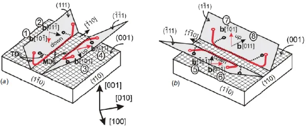
For Ge eight slip systems exist for 60°dislocations, which are schematized in Figure 2.4 [48]. Two pairs of orthogonal {111} glide planes exist, each plane presenting a MD at the epilayer-substrate interface and two different TDs propagating in the epilayer along the preferential <110> directions.
Figure 2.4: Schematic representation of the eight slip systems existing for 60° dislocations in Ge epitaxial layers grown on (001) Si. After Ref. [48].
11
Edge 90° MDs with Burgers vector and dislocation line in the plane of the epilayer-substrate interface would represent the most effective kind of dislocation to accommodate the strain in the growing epilayer, as in this case the crystal deformation is exactly in the plane of the interface. However, the (001) plane is not a glide plane for dislocations, so that 90° MDs are non-moving dislocations, or sessile dislocations. As a consequence, the nucleation of pure edge MDs is energetically unfavorable compared to the formation of mobile (glissile) 60° MDs [48]. The screw component of such dislocations causes the degradation of the epilayer not just in the interface region but also at large distance from it. Even though 90° MDs have low formation probability, these defects are observed in large quantities in annealed Ge epilayers grown on Si. One model to account for this considers that, during gliding, two 60° dislocations can interact and form one 90° MD if the sum of the Burgers vectors of the original MDs has no component in z direction (the direction of film growth) as in the proposed reaction:
𝑎𝐺𝑒 2 [101̅] + 𝑎𝐺𝑒 2 [011] = 𝑎𝐺𝑒 2 [110] 2.7
The resulting dislocation line lies at the intersection of the {111} gliding planes and has an orthogonal Burgers vector which is in a plane parallel to the interface. Annealing of Ge on Si substrates, which causes the motion of existing dislocations due to expansion and contraction of the Ge lattice, promotes the interaction of 60° dislocations which can combine to form pure edge 90° MDs, while TDs result actively annihilated.
In absence of non-equilibrium concentrations of point defects and at low temperatures where diffusion is difficult, the movement of dislocations is limited on the {111} glide planes. With increasing annealing temperature, the density and length of MDs is found to increase [49]. The velocity of glide 𝑣𝑔 of dislocations, which is a thermally activated process, can be expressed as [50]:
𝑣𝑔 = 𝐵𝜀 𝑒−𝐸𝐾𝑇𝑔 2.8
where 𝐵 is a constant value, 𝑇 is the annealing temperature and 𝐸𝑔 is the glide energy barrier which is 1.6 eV for bulk Ge.
12
2.4 Main challenges in Ge epitaxy on Si
The main requirements for high-quality Ge on Si VSs useful for device integration are a low threading dislocation density (TDD), complete relaxation, a low surface roughness, the absence of cracks and a controlled bowing. High degree of relaxation close to 100% is necessary in order to avoid subsequent epilayer relaxation during further wafer processing, which could promote the further nucleation of TDs in the grown epilayers degrading their electrical properties. Cracks can originate in the Ge epilayer during cooling down the VS from growth temperature to room temperature, as a consequence of the large thermal expansion coefficient mismatch of 125% existing between Ge and Si (∝Si= 2.6 x 10⁻⁶ K−1 and ∝Ge= 5.8 x 10⁻⁶ K−1 at 300 K) and they can be eliminated by
adjusting the process conditions. Low TDD and surface roughness are hampered by the large lattice mismatch existing between Ge and Si, which leads to the nucleation of a large number of dislocations in the order of 1010-1012 cm-2 at the growth interface which thread in the upper layers [51] and to S-K island growth.
When Ge on Si VSs are used as a platform for subsequent epitaxial growth of III-V semiconductors it is necessary to take into account the polar on non-polar nature of the epitaxial process. The growth of III-V semiconductors on (001) oriented group IV semiconductors typically leads to the formation of antiphase domains (APDs) and associated antiphase boundaries (APBs), the latter acting as preferential centers for minority carrier recombination thus degrading minority-carrier lifetime [52, 53]. The use of vicinal Si substrates, characterized by a surface which is not flat but constituted by many terraces separated by atomic steps, hamper the formation of APDs and APBs thanks to a layer by layer Ge growth which proceeds by completion of existing terraces. Typically, (001) vicinal Si wafers with 6° offcut towards [111] direction are used as starting substrates for Ge epitaxy when the grown VSs are used as a platform for the subsequent growth of III-V semiconductors. While the use of 6° offcut Si wafers can effectively suppress the formation of APDs and APBs in the upper III-V semiconductors [54], their use increases both the dislocation content and Ge RMS roughness compared to the case of Ge grown on 0° offcut Si wafers. This is mainly attributed to an imbalance in Burgers vectors for Ge grown on 6° offcut Si, which promote dislocation nucleation over annihilation [55].
To allow the integration of III-V semiconductors, Ge on Si VSs with a maximum TDD ~106 cm-2 are required. This TDD represents the threshold value for which the lifetime of minority carriers in n-type GaAs grown on Ge on Si VSs is comparable with that of the same semiconductors grown on lattice matched substrates (see Figure 2.5, after Ref. [56]).
13
Figure 2.5: Lifetime of electrons and holes minority carriers as a function of TDD in GaAs epilayers grown on Ge on Si VSs. After Ref. [56]
2.5 Assessment of threading dislocation density
TDs represent the main issue in Ge epitaxy on Si so that an assessment of TDD within grown Ge epilayers is of extreme importance. The main used techniques to assess the density of threading dislocations in heteroepitaxial layers are both plan-view and cross sectional transmission electron microscopy (TEM), etch pit density (EPD) and high-resolution X-ray diffraction (HR-XRD).
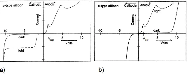
TEM cross sectional (XTEM) analysis is a powerful technique for defects visualization and is only limited by the small viewing area. Typical sample dimensions which can be investigated are about 20µm of width and 0.7 µm of depth, corresponding to a maximum observable area of about 10-7 cm-2 [57]. As a consequence, the observation of threading dislocations using TEM is only significant for threading dislocation densities above about 107cm-2 and for lower TDD values EPD is typically employed. EPD is the easiest way to reveal dislocations, which employs preferential etching and inspection of the resulting etch pits using an optical microscope or an atomic force or scanning electron microscope. The sample is treated with an etching solution which comprises an oxidizer (HNO3, H2O2, K2Cr2O7, CrO3), a complexing agent (HF) and a diluent (water or organic solvents). The etch pits, which are created due to the preferential oxidation and removal of material in the strain field which surround each dislocation, are formed in correspondence to the crossing point of the dislocation line with the surface of the sample. TDD at sample surface is determined by counting the pits across a known area and the higher dislocation density that can be determined in this way is about 108 cm-2 because for higher density
14
the etch pits start to overlap. In this case the dislocation density is usually determined through XTEM analysis. EPD technique typically gives a lower limit for the threading dislocation density because dislocations which run parallel to the surface can't be detected and single dislocations can’t be resolved if dislocation pile-ups occurs. Even though the sample preparation for X-TEM analysis is very long, this technique can provide a wealth of information about sample morphology, allowing for observation of single defects, their structure and propagation. Compared to X-TEM, plan-view TEM analysis has the advantage of a faster sample preparation and of the possibility to observe a much larger area of the sample, so that a minimum observable defects density in the order of 105 cm-2 can be assessed using this technique. In this thesis TDD will be assessed using both plan view TEM analysis and EPD.
HR-XRD is a not-destructive technique which can provide a lot of structural information about grown epilayers such as lattice constants, crystallographic orientations, strain and tilt together with defect density [58]. Typically, rocking curve (RC) analysis is carried out to assess the TDD in heteroepitaxial layers, by studying the dislocation induced broadening of the full-width at half maximum (FWHM) of one or different families of diffracting planes, after deconvolution of the collected signal from other broadening effects [58]. Since RC analysis is expected to have a minimum sensitivity for dislocation density in the order of 5 x 105 cm-2 [59], it is perfectly suitable for dislocation assessment in pure Ge on Si heterostructures, where an average dislocation density in the whole Ge epilayer in the order of 105 cm-2 represents an extremely low value perfectly suitable for subsequent epitaxial growth. For direct Ge integration on Si, a TDD at Ge surface > 106 cm-2 is typically obtained and in these conditions primary and secondary extinction of X-rays are often negligible, causing X-X-rays to penetrate several µm within the epitaxial layer [60]. As a consequence, the whole epilayer thickness results investigated during RC analysis and the obtained TDD represents an average value which also takes into account the highly dislocated Ge/Si interface.
2.5.1 High Resolution X-Ray diffraction analysis (HR-XRD)
Different models have been proposed to assess the TDD in heteroepitaxial layers studying the broadening of the diffraction peak of a single or multiple families of atomic planes. At first, Gay and Hirsh develop a model for TDD assessment in annealed metals, which reported an upper limit for total dislocation density which depends on the ratio (𝐹𝑊𝐻𝑀3⨯𝑏 )2[61]. An empirical correlation between TDD at Ge surface and the change in measured FWHM before and after EPD analysis was reported by Sous and collaborators
15 [62], which found a TDD dependence on 𝐶 ⨯ (𝐹𝑊𝐻𝑀
3⨯𝑏 ) 2
, where 𝐶 is a correction factor <1. Successively, Ayers extended the model of Gay and Hirsh to heteroepitaxial layers by considering the diffraction peaks as Gaussian functions resulting from the convolution of different Gaussian intensity distributions given by: the intrinsic rocking curve of the layer being examined, the instrumental broadening, finite thickness broadening, curvature broadening and dislocation broadening [63]. Later, Kaganer et al. shown that MDs and TDs have similar effects on the broadening of the epitaxial layer diffraction peaks, making it difficult to assess the TDD from FWHM broadening [64]. However, very recently Kopp, Kaganer and collaborators demonstrated the contribution of MDs on the FWHM broadening is negligible, so that TDD can be effectively determined from the broadening of collected diffraction peaks without the need to consider the effect of MDs [65].
The model proposed by Ayers was successfully applied to the GaAs/Si epitaxial system, since the GaAs diffraction peaks for different families of scattering planes are very well approximated by Gaussian functions, with the exception of the tail regions which are typically underestimated by the Gaussian fit. However, only small diffracted intensity is found in the tails so that the model does not introduce significant sources of errors in this case [63, 66]. On the other hand, the application of the same model to the Ge/Si epitaxial system is not straightforward, as the good agreement existing between GaAs diffraction peaks and Gaussian approximation is not valid for the Ge diffraction peaks. The (004) diffraction peak for a Ge epilayer integrated in silicon via a porous buffer is reported in Figure 2.6, together with the best Gaussian function approximating the peak. Similar results have been obtained for different families of scattering planes both in presence and absence of a porous buffer layer in between Ge an Si. The Gaussian function underestimates both the tail regions as well as the central region of the diffraction peak, where most intensity resides.
It follows that the assumption of a Gaussian distribution would lead to an overestimation of the Ge FWHM, and a consequent overestimation of TDD. For an accurate analysis of the TDD within Ge by means of HR-XRD techniques, more complex functions such as Lorentzian function and Voigt function should be used to fit the Ge diffraction peak [67].
16
Figure 2.6: (004) Ge RC for Ge grown on pSi and its best Gaussian approximation (in red). Deviations from the ideal Gaussian behavior are found in the tail regions as well as in the central region of the Ge diffraction peak.
While an assessment of TDD by using HR-XRD is not straightforward for Ge epilayers, it is possible to determine in an approximate manner the relative change in TDD for two Ge on Si VSs, provided that TDs represent the only non-negligible contribution to FWHM broadening.
In this case the relative change in TDD can be expressed as:
TDD1 TDD2= ( FWHM1 FWHM2) 2 2.9
where TDD1 and TDD2 represent the TDD for sample 1 and 2, while FWHM1 and FWHM2 represent the FWHM of a selected family of scattering planes for sample 1 and 2, respectively. The dependence of TDD on FWHM2 has been observed for both Gaussian
[58, 63, 66] and non-Gaussian [61, 62] diffraction peaks, suggesting that Eq. (2.9) can be applied to non-Gaussian Ge epilayers without introducing a large error. Eq. (2.9) will be used to assess the change in TDD in presence and absence of a compliant porous buffer in the VSs structure, while a quantitative analysis of TDD will be carried out using TEM plane view analysis and EPD, in combination with scanning electron microscopy (SEM) imaging.
17
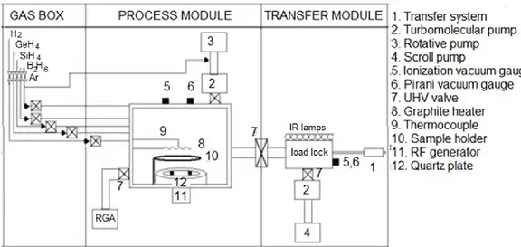
2.6 Low energy plasma enhanced chemical vapor deposition
(LEPECVD)
The large-scale fabrication of Ge on Si VSs requires a growth technique which can take advantage of very high growth rates, thus allowing for high throughputs. Low energy plasma enhanced chemical vapor deposition (LEPECVD), which is an epitaxial technique developed for the growth of Ge, Si and SiGe alloys at very high deposition rates up to 10 nm/sec, represents the ideal technique from this point of view [68]. Despite the very high achievable growth rate, which is more than 10 times faster than other epitaxial techniques such as MBE and ultra-high vacuum CVD (UHV-CVD), epitaxial layers grown by LEPECVD presents similar or better electrical properties compared to those grown with other techniques [69].
In LEPECVD non-thermal energy is furnished by a dense and low-energy plasma for the dissociation of the reactive molecules, so that very low substrate temperatures can be adopted during epitaxy the same being not possible for thermal techniques. The generated plasma promotes the formation of highly reactive radicals and energetic ions, which strike the sample surface and cause a great enhancement of the hydrogen removal rate, which in turn leads to the above mentioned high growth-rate. The arrival of energetic ions on the sample surface leads also to an enhancement in the particles mobility, which is of great importance when epitaxial growth is performed at low thermal budgets. The PECVD process investigated in this thesis is based on radio-frequency inductively coupled plasma (ICP) excitation at the frequency of 13.56 MHz inside a quartz chamber embedded in the high vacuum reactor. This process, also known as radio frequency plasma enhanced chemical vapor deposition (RF-PECDV), differs from other PECVD techniques because the substrate is not biased and ions are accelerated in every direction. Plasma formation involves the generation of an alternate current in an aluminum antenna, which in turn result in the formation of a variable magnetic field. This magnetic field generates a variable electric field in orthogonal direction which accelerates the electrons of the carrier gases introduced in the growth chamber promoting plasma formation. To start the plasma reaction H2 or Ar gases are typically fluxed in the growth chamber while precursor gases are added in a subsequent moment, when the plasma is already generated. All the samples realized in this thesis work have been grown using H2 to start the plasma reaction and as carrier gas, which is introduced in the growth chamber in proximity of the antenna. In the LEPECVD reactor located in the cleanrooms of the Physics and Earth Science Department at Ferrara University the plasma source is located in the bottom part of the growth chamber and the samples are introduced in the reactor facing down, in order to avoid dust to fall and accumulate on the Si polished
18
surface. A graphite heater positioned a few centimeters above the wafer provides it the necessary thermal energy during epitaxial growth. Typical growth temperatures for pure Ge epilayers are in the range 400 to 600°C and a constant temperature of 500°C is employed for the samples grown in this thesis.
Germane (GeH4), is used as precursor gas and is introduced in the growth chamber through a gas ring positioned just below the Si substrate. Using a turbo molecular pump and a rotary pre-vacuum pump the main chamber of the LEPECVD reactor is pumped at a base pressure of 2 x 10⁻⁸ mbar, while during the deposition process the working pressure is 2 x 10⁻² mbar. A load lock prevent contamination of the growth chamber during wafer loading and, thanks to a set of IR lamps, promotes desorption of residual diluted HF from Si wafer surface after native oxide removal. During epitaxy the energy of the ions incoming on the substrate should be lower than 15 eV, in order to avoid the formation of bulk defects and the formation of stacking faults which could eventually lead to a polycrystalline growth [69]. A schematic representation of the LEPECVD system used in this work is reported in Figure 2.7. Together with the reduced thermal budget and high growth rates, another great advantage of LEPECVD over conventional techniques is the possibility to suppress island formation in Ge epilayers on Si, by taking advantage of out-of-equilibrium growth conditions [9].
19
2.7 First experimental results
At the beginning of this thesis work several attempts have been made to grow monocrystalline Ge epilayers on bulk Si, resulting in strongly polycrystalline Ge as assessed from very broad (004) ω–scan FWHM values in the order of 2000 arcsec for 5 µm-thick Ge epilayers, and to the lack of the Ge diffraction peak in ω/2θ scans collected in triple axis diffraction mode. The main cause for this polycrystalline growth has been ascribed to the incomplete desorption of water from wafer surface before epitaxial growth. The desorption time in the load lock has been than increased from 5 minutes at 150°C to 10 minutes at 200°C, resulting in monocrystalline Ge epilayers on bulk Si and (004) FWHM in the order of 1000 arcsec or less. However, desorption of hydrogen and other adsorbed species from bulk Si and porous Si internal surface was observed at temperatures > 400 °C [70, 71], which is much larger than the maximum desorption temperature of 200°C possible in the load lock in the present reactor configuration. As a consequence, complete water desorption for the samples grown during this thesis’s work has been carried out within the main reactor chamber, possibly introducing here some contaminants.
Despite the high growth rate of several nm/sec obtainable using LEPECVD, in the present configuration the maximum wafer throughput is limited to 0.5 wafer per day as a consequence of the necessity to perform a NF3 plasma cleaning after each single growth to remove the germanium accumulated within the growth chamber and restore a base pressure of 2 x 10⁻⁸ mbar before successive growth, as the non-thermal dissociation of GeH4 leads to Ge deposition not only on the starting substrate but also on the chamber sidewalls and other mechanical parts. In particular, it is believed that germanium accumulated on the quartz shield used to protect the aluminum antenna used to generate the plasma from the plasma itself shields the H2 carrier gas from the variable electric field generated by the antenna, thus hampering plasma formation. About 1 hour NF3 cleaning resulted hence necessary in order to remove the accumulated Ge as the growth of two 5µm-thick Ge epilayers without intermediate plasma cleaning step resulted in the impossibility to start again the plasma and the necessity to expose in air the reactor chamber and clean manually the quartz shield. A different reactor configuration is mandatory in which no plasma cleaning is necessary after epitaxy in order to take full advantage of the high growth rates typical of LEPECVD technique.
20
Chapter 3
Porous silicon buffer layers
3.1 Introduction
In the last years there has been an increasing interest towards nanostructured systems and their application in microelectronic and optoelectronic devices as new physical properties appears when the physical dimensions of a structure becomes smaller than a characteristic length scale. Although photolithography represents one of the main techniques for the realization of nanostructured devices, self-assembled structures are of great interest because of their simpler fabrication processes, which can lead to higher throughputs while decreasing fabrication costs [72].
As silicon represents the most widely used semiconductor for microelectronic applications, Si based nanostructures are of particular interest because of their enhanced functionality and compatibility with CMOS technology. In particular, porous silicon (pSi) is a very versatile self-organized material which mechanical, optical, transport and absorption properties can be finely tuned by modifying the growth parameters. pSi was discovered by Uhlir in 1956 during experiments concerning the electropolishing of silicon however, is only from the 1990 that pSi started to be extensively investigated as a consequence of the discovery of room-temperature photoluminescence in nanoporous silicon layers [73]. pSi presents peculiar characteristics which can be exploited in a wide range of optoelectronic and microelectronic devices such as light-emitting diodes [74], gas sensors [75], transistors [76], photodetectors [77], waveguides [78], modulators [79] and solar cells [80, 81]. In particular, for what concerns solar cell applications, electrochemically etched pSi layers have been investigated as anti-reflection coating for high efficiency devices [82] and pSi multilayers have been proposed as Bragg reflectors in thin-film Si solar cells [83] or for lift-off of ultra-thin Si solar cells for wafer reuse [84]. Even though deep investigation of pSi started around 25 years ago, there is renewed interest towards this material due the possibility of monolithical integration with electronics on one chip, to its simple and easy preparation, and to the existence of an extremely broad space parameter for pore formation, making pSi properties tunable over
21
a very large interval which is not fully explored up to date [85]. Moreover, also the high-throughput and low-cost of electrochemical etching process and its scalability to large wafers play an important role in making porous silicon an appealing candidate for novel microelectronic and optoelectronic applications.
3.2 Fabrication and characterization of porous silicon
Two main techniques exist for the fabrication of porous silicon layers: electrochemical etching and stain etching. While electrochemical etching is based on holes availability at the interface between Si and the electrolyte, stain etching consists in etching of Si using an aqueous solution which involves HF and an oxidizing agent e.g. HNO3. Among these two techniques stain etching of Si allows higher throughputs, as a whole batch of wafers can be etched at the same time, the same being not possible through electrochemical etching which requires the realization of an electric contact for each single wafer to be processed. Even though stain etching can take advantage of extremely high throughputs, stain etched substrates typically result in porous layers of low homogeneity and poor reproducibility making this technique difficulty applicable in an industrial environment [86]. This is mainly a consequence of the fact that in stain etching the already porosified porous layer is continuously attacked by the HF based solution as the process continues, so that the porous layer starts to dissolve for long etching times. It follows that the porosity of stain etched porous layers decreases with the depth of the porous layer [86]. This is not the case of electrochemical etching, where the already porosified region is fully depleted of holes and results hence passivated, so that thick porous layers can be realized without degradation of the pSi surface. In practice, however, together with electrochemical etching slow pure chemical dissolution of pSi in HF containing electrolyte occurs. Pure chemical etching of pSi does not require hole availability to proceed and its effect increases with increasing residence time of pSi in HF solutions. In contrast with stain etched porous layers, in electrochemically etched layers grown at fixed current density, and when pure chemical etching is negligible, the porosity increases with the thickness of the porous layer. This is a consequence of the reduced density of F- ions which reach the pore tip for increasing depth of the porous layer.
In this thesis porous silicon will be investigated as possible buffer layer for germanium heteroepitaxy. Since the surface quality of the starting substrate is of foremost importance in epitaxial processes, only electrochemical etched porous layers will be here investigated.
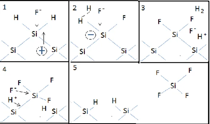
![Figure 3.5: Thickness and porosity of grown pSi layers as a function of provided current density for 20s anodization time of 3.9mΩcm p-type Si (001) oriented with 6° offcut towards [111]](https://thumb-eu.123doks.com/thumbv2/123dokorg/4728336.45969/43.892.227.666.407.681/figure-thickness-porosity-function-provided-density-anodization-oriented.webp)