RRAM Reliability/Performance Characterization
Through Array Architectures Investigations
Cristian Zambelli, Alessandro Grossi, and Piero Olivo
Universit`a di Ferrara, Dipartimento di Ingegneria, ENDIFVia Saragat 1, Ferrara, 44122, Italy E-mail: [email protected]
Christian Walczyk, and Christian Wenger
IHP MicroelectronicsIm Technologiepark 25, 15236 Frankfurt (Oder), Germany E-mail: [email protected]
Abstract—The reliability and performance characterization
of each non-volatile memory technology requires the thorough investigation of dedicated array test structures that mimic the real operations of a fully functional integrated product. This makes no exception also for emerging non-volatile memories like the Resistive Random Access Memory (RRAM) concept. An extensive electrical characterization activity performed on test vehicles manufactured in a CMOS backend-of-line process allowed the first glance estimation of operation modes and reliability threats typical of this technology. In this paper, it is provided a review of the most important issues like form-ing instabilities, optimal set/reset operation findform-ing, and read disturb to provide a guideline either for a further technology optimization or an efficient algorithms co-design to handle these reliability/performance threats.
Index Terms—RRAM; test-structures; array; reliability;
per-formance
I. INTRODUCTION
The Resistive Random Access Memories (RRAM) are a promising candidate to become a key memory technology in several applications. From a technological standpoint, em-bedded HfO2-based RRAM devices are interesting because
they offer compatibility with the standard CMOS backend-of-line (BEOL) process scheme and very fast operation times, mostly below the 100 ns limit. Extensive characterizations have been performed in the framework of a concept-validation for possible replacement of existing non-volatile memory technologies, trying to ease the evolution from single cell test structures to fully functional integrated array products [1]–[4]. In the last decade, most of the analysis, especially those devoted to provide a solid understanding of the physical mech-anisms ruling the RRAM operations, have been performed on simple 1T-1R architectures where a select transistor or a diode is connected in series to the resistive element [3]. However, although this demonstrated competitive features with respect to the traditional floating gate-based Flash technology, single devices are not ideal to study the statistical distribution of the inter-cell variability of memory elements. Moreover, that solution does not allow a thorough characterization of the typical issues evidenced in a memory product such as disturbs, cells interaction, sub-optimal writing algorithms or cell faults due to process induced variability.
In this work we will present a review of the most important issues retrieved during the electrical characterization of 4kbits
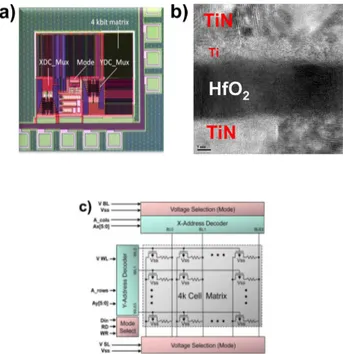
Fig. 1. Microphotograph of the 4kbits memory array with control circuits (a). Cross-Sectional STEM Image of the integrated MIM stack in the ReRAM Cell (b). Simplified block diagram of the memory array (c).
RRAM memory array test structures with the associated control circuitry designed in a 0.25 µm BiCMOS technology node [5]. The results will show that some important reliability threats that could severely limit the ramp-up of the RRAM arrays toward a technology mature level, can be addressed by simply acting on the operative conditions of the cells within the array and on the algorithms that handle the read/write operations. The common analysis performed in these test arrays are mainly related to the evaluation of the performance and of the reliability features of the technology, through the application of voltage/current waveforms at dedicated test pads for the following operations: forming, set, reset, and read. The applied waveforms shape, duration, and amplitude determine the behavior of the array either on a short time-scale (e.g., characterization of the read window, determination of the variability, etc.) or on a longer time-scale (e.g., endurance and retention evaluations).
© 2015 IEEE. Personal use of this material is permitted. Permission from IEEE must be obtained for all other uses, in any current or future media, including reprinting/republishing this material for advertising or promotional purposes, creating new collective works, for resale or redistribution to servers or lists, or
reuse of any copyrighted component of this work in other works.
This is the accepted version of the paper. The published version can be found at http://ieeexplore.ieee.org/document/7309588/ The DOI of the published version is: 10.1109/ISVLSI.2015.17
II. TEST VEHICLE MANUFACTURING
The structure of the 4kbits memory array (see Fig. 1) is described by four architectural blocks: the array of 4096 1T-1R RRAM cells; a wordline (WL) address decoder (XDC MUX); a bitline (BL) address decoder (YDC MUX); and an operation control circuitry (Mode) to handle read and write operation commands. The memory cells are constituted by a select NMOS transistor featuring W=1.14µm and L=0.24 µm in series to a variable resistor connected to the bitlines.
The variable resistor is a Metal-Insulator-Metal (MIM) stack fabricated on 150 nm TiN bottom electrodes deposited by magnetron sputtering with sheet resistances in the order of 10-50 Ωsq−1 directly on the last metallization of the BiCMOS
process. Next, HfO2 films of 9nm thickness were grown in
an AVD chamber at 320 ◦C using Hf[N(MeEt)]4 precursor
and O2 as reactive gas. Finally, 10 nm Ti and 150 nm TiN
were sputtered onto the HfO2layer [6], [7]. To investigate the
impact of the MIM area on the memory performances and variability two different arrays have been integrated using 0.6 µm2
and 1 µm2
resistor area, respectively.
III. FORMING OPERATION VARIABILITY AND INSTABILITIES
RRAM behavior is based on the possibility of electrically modifying the conductance of a Metal-Insulator-Metal (MIM) stack: the Set operation switches the cell into a high conductive state, whereas Reset brings the cell back to a low conductive state. Some technologies like HfO2-based RRAM require a
preliminary forming operation to activate such a switching behavior by creating a conductive filament (CF) in the di-electric material [5], [8]–[10]. Even if such forming process is performed just once, it plays a fundamental role in determining the system performance [10]. A deep understanding of the forming process allows recognising faulty cells in the array from scratch and to get a first glance insight on the cells reliability and performances during lifetime. Forming usually consists in the application of a quasi-DC sweep on the BL up toVBL= 3.5 V with step voltage equal to 0.025 V. To prevent
hard breakdown, the saturation current of the select transistor is controlled by the WL voltage fixed atVW L= 1.4 V, which
translates into a compliance current almost equal to 300µA. The forming process in the array could be accelerated by selecting multiple rows and/or columns simultaneously using the Mode circuitry. After the operation it is possible to read the array content by applyingVW L= 1.4 V and a read voltage
VBL considerably lower than the switching voltages requested
for the set and reset operations.
Fig. 2 depicts the variability of the forming voltage distri-bution and the cumulative probability data of the read currents measured on the entire array before and after the forming operation. The large variability in forming voltages indicates the peculiar behavior for each of the cells in the array. Before forming the read currents are distributed around a mean value µ = 4.03 µA with a standard deviation σ = 0.48 µA, whereas after forming the average current were distributed aroundµ = 30.31 µA with a standard deviation σ = 0.23 µA. These
2 2.5 3 3.5 VBL [V] 0 200 400 600 800 Cells [#]
Fig. 2. Forming voltage distribution (left) and distributions of the read current in a ReRAM array with 1µm2
MIM area before and after forming (right) [7].
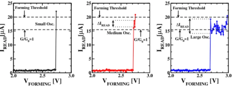
2.0 2.5 3.0 VFORMING [V] 0 5 10 15 20 25 IREAD [µ A] Forming Threshold Small Osc. G/G0=1 2.0 2.5 3.0 VFORMING [V] 0 5 10 15 20 25 IREAD [µ A] Forming Threshold ∆IREAD Medium Osc. G/G0=1 2.0 2.5 3.0 VFORMING [V] 0 5 10 15 20 25 IREAD [µ A] Forming Threshold ∆IREAD Large Osc. G/G0=1
Fig. 3. Three different behaviors observed during forming process: small (left), medium (centre) and large (right) read-verify current oscillations [11].
results are obtained on arrays based on 1 µm2
MIM area, however similar results are found in 0.6µm2
MIM area arrays. The analysis of the pre-forming distribution allows an indirect insight on the process induced variability in the MIM stack. In this technology, pre-forming currents larger than 10 µA usually indicate leaky cells due to fabrication issues such as the intrinsic variability of the HfO2 deposition process [5]. This
source of variability is also responsible for forming failures (i.e., cells that are unable to be formed), which is considered as a major contribution for the array yield loss (i.e., 40% of the cells in the array). A possible solution for this reliability threat has been proposed in [7] by using a forming-retry operation on the cells that are not able to create a CF, increasing the yield up to 99%.
Another issue retrieved during forming operation is the intrinsic instability of the created CF that could impact on the successive set/reset switching operations [11]. Indeed, by monitoring the cells forming behavior through an incremental pulse forming technique it is observed that the read current during forming could exhibit, in some cells, an oscillatory behavior (see Fig. 3). These oscillations interpreted either as the charging of a trap close to the surface of the conductive filament (CF) or the movement of an atom/defect in the filament [12], has been investigated in terms of reliability and cell-to-cell variability during 1k endurance cycles and 100k stress pulses in different cycling conditions.
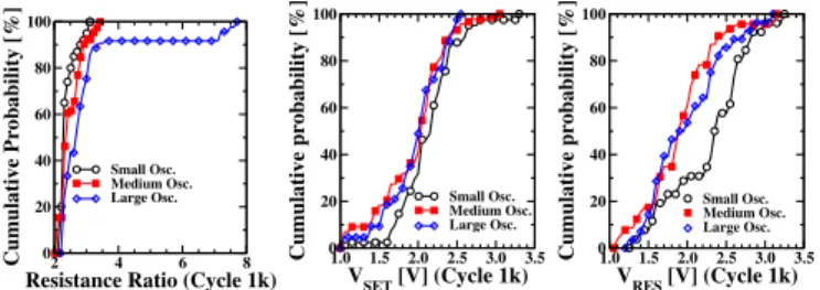
Fig. 4 shows the cumulative distributions of the resistance ratio, set and reset switching voltages calculated after cy-cling. Resistance ratio is calculated as the ratio of the set state read current and reset state read current ILRS/IHRS at
Vread= 0.2V . The cells formed with smaller oscillations are
shown to require higherVSET andVRES after 1k cycles: that
means small oscillations correspond to wider filaments. The Resistance Ratio,VSET,VRES average values and dispersion
2 4 6 8
Resistance Ratio (Cycle 1k)
0 20 40 60 80 100 Cumulative Probability [%] Small Osc. Medium Osc. Large Osc. 1.0 1.5 2.0 2.5 3.0 3.5 VSET [V] (Cycle 1k) 0 20 40 60 80 100 Cumulative probability [%] Small Osc. Medium Osc. Large Osc. 1.0 1.5 2.0 2.5 3.0 3.5 VRES [V] (Cycle 1k) 0 20 40 60 80 100 Cumulative probability [%] Small Osc. Medium Osc. Large Osc.
Fig. 4. Resistance ratio, VSET, VRES cumulative distributions for the
different forming oscillations groups calculated on cycled devices [11].
100 101 102 103 Switching Cycles 2 2.5 3 3.5
Resistance Ratio Small Osc. (µ)Medium Osc. (µ)
Large Osc. (µ) 100 101 102 103 Switching Cycles 1.5 2 2.5 VSET [V] Small Osc. (µ) Medium Osc. (µ) Large Osc. (µ) 100 101 102 103 Switching Cycles 1.5 2 2.5 VRES [V] Small Osc. (µ) Medium Osc. (µ) Large Osc. (µ) 100 101 102 103 Switching Cycles 0 0.1 0.2 0.3 0.4 0.5 0.6 0.7 0.8 0.9 1
Ratio Dispersion Coeff.
Small Osc. Medium Osc. Large Osc. 100 101 102 103 Switching Cycles 0 0.05 0.1 0.15 VSET Dispersion Coeff. Small Osc. Medium Osc. Large Osc. 100 101 102 103 Switching Cycles 0 0.05 0.1 0.15 VRES Dispersion Coeff. Small Osc. Medium Osc. Large Osc.
Fig. 5. Resistance Ratio,VSET andVRESaverage values and dispersion
coefficients calculated during cycling [11].
0 5 10 15 20
IREAD [µA] (Small Osc.)
0 20 40 60 80 100 Cumulative Probability [%] HRS Pulse 1 Pulse 1k Pulse 100k 0 5 10 15 20
IREAD [µA] (Large Osc.)
0 20 40 60 80 100 Cumulative Probability [%] HRS Pulse 1 Pulse 1k Pulse 100k
Fig. 6. Cumulative distributions of the read currents (withVread= 0.2V )
measured during set stress on HRS after different number of disturb pulses, at endurance cycle 1 [11].
coefficients calculated during cycling are reported in Fig. 5. To evaluate the cell-to-cell variability the dispersion coefficient ofILRS andIHRS distributions, defined as (σ2/µ), has been
used. Resistance ratio of cells with large forming oscillations show both higher average value and dispersion coefficient in all cycling conditions: that means large fluctuations corre-spond to narrower filaments.VSET,VRES average values and
dispersion coefficients are shown to increase during cycling: switching voltages on cells formed with large oscillations show lower average values and dispersion in all cycling conditions. This indicates cells with lowerVSET,VRES have a not fully
developed filament: this explains the large fluctuations. One
5 10 15 20 25 30
I
READ [µA] (Small Osc.)
0 20 40 60 80 100 Cumulative Probability [%] LRS Pulse 1 Pulse 1k Pulse 100k 5 10 15 20 25 30
IREAD [µA] (Large Osc.)
0 20 40 60 80 100 Cumulative Probability [%] LRS Pulse 1 Pulse 1k Pulse 100k
Fig. 7. Cumulative distributions of the read currents (with Vread= 0.2V )
measured during reset stress on LRS after different number of disturb pulses, at endurance cycle 1 [11].
reason of the parameters dispersion could be the root mean square surface roughness of HfO2 films due to the columnar
structure of the TiN bottom metal electrode [13].
To evaluate the disturbs immunity of each cells group, 100k reset stress pulses have been applied after set with Vstress,res = 0.8V , Tstress,res = 10µs and 100k set stress
pulses after reset with Vstress,set = 0.8V ,Tstress,set = 10µs
at different cycles. Set/reset stress voltage pulses with 0.8V have been used since it’s almost half of the average set/reset switching voltage measured on fresh devices. Cumulative distributions of the read currents measured after reset (HRS), set (LRS) and during set and reset stress on fresh devices are reported in Fig. 6 and Fig. 7, respectively: in both cases cells formed with larger current oscillations show a lower disturb immunity. That reveals larger fluctuations indicate a not so well formed filament thus more prone to exhibit lower immunity.
All these findings summarize the importance of the forming operation in the lifetime of a RRAM array.
IV. OPTIMALSET/RESETOPERATION
The average set and reset characteristics in a RRAM array feature the same variability observed in forming [6], [14]. Moreover, as usually evidenced in RRAM technology [1], the read current IHRS shows a larger range of variability
com-pared toILRS, as evidenced in Fig. 8 showing the cumulative
distributions of the set/reset switching voltages calculated on the entire array. These results indicate that an optimization of the set/reset operations is mandatory to reduce the impact of the device variability, whereas minimizing the array yield loss due to non-switching cells. To this purpose, the analysis in [15] compared DC and pulsed set/reset operations featuring different durations and voltages. A set of 10000 set/reset cycles has been considered for the analysis.
SET operation in DC mode has been performed increasing the bitline voltage VBL from 0 to 3.5V with Vstep = 0.1V
(Tstep,DC = 50µs) and the wordline voltage fixed to VW L
= 1.4V. RESET operation in DC mode has been performed increasing the source line voltage VSL from 0 to 3.5V, with
Vstep = 0.1V (Tstep,DC = 50µs) and VW L = 2.5V. In pulsed
0.5 0.75 1 1.25 1.5 1.75 2 2.25 2.5 2.75 3 Switching Voltage [V] 0.1 1 10 10 50 50 90 99 99.9 Cumulative Probability [%] RESET SET µRES = 1.91 V σRES = 0.25 V µSET = 1.52 V σSET = 0.18 V
Fig. 8. Cumulative distribution of the set and reset switching voltages in the entire RRAM array [15].
1 10 100 1 k 10 k SET/RESET Cycle [#] 0.5 0.75 1 1.25 1.5 1.75 2 Normalized I HRS /ILRS DC-Mode TPULSE=50µs TPULSE=10µs TPULSE=1µs 0 10 20 30 40 50 60 70 80 90 100 Switching Yield [%] DC-Mode T PULSE=50µs T PULSE=10µs T PULSE=1µs a) b)
Fig. 9. Normalized read current Ratio (a) and Switching Yield (b) evaluation for different set/reset modes (DC and pulses with different durations) during cycling. Vpulse= 3V for pulsed modes [15].
1 10 100 1 k 10 k SET/RESET Cycle [#] 0.6 0.8 1 1.2 1.4 1.6 1.8 2 Normalized I HRS /ILRS VPULSE = 3.5V VPULSE = 3V V PULSE = 2.5V 0 10 20 30 40 50 60 70 80 90 100 Switching Yield [%] V PULSE = 3.5V VPULSE = 3V V PULSE = 2.5V TPULSE = 10µs a) b)
Fig. 10. Normalized read current Ratio (a) and Switching Yield (b) for different set/reset pulse amplitudes during cycling. Tpulse= 10µs [15].
= 1.4V during SET and VW L = 2.8V during RESET, while
different bitline/sourceline voltages and durations have been investigated.
In Fig. 9 a comparison between DC and pulsed mode with different durations at fixed Vpulse = 3V is depicted.
Fig. 9a shows IHRS/ILRS, normalized with respect to that
calculated at cycle 1, as a function of the set/reset cycle
1 10 100 1 k 10 k
SET/RESET Cycle [#]
0 5 10 15 20 25 30I
READ[
µ
A]
RESET SET AGGRESSIVE AVERAGEFig. 11. Set and reset read current behavior during cycling with Vpulse=
3V,Tpulse= 10µs. Average and aggressive read window calculation points
are indicated [15].
number for different pulse durations. In all cases a non-monotonic behavior is observed, eventually ending up with a significantIHRS/ILRS reduction with the exception of the
shortest pulse duration (Tpulse = 1µs). Fig. 9b shows the
switching yield (i.e., the percentage of cells in the array that actually toggles between set/reset states) of each set/reset mode providing an interesting trade-off: pulses with a too short or too long duration result in a lower yield compared to an average timing condition. Similar considerations can be derived by the analysis of Fig. 10, where the dependencies of the normalizedIHRS/ILRSand that of the switching yield are
evaluated in cycling for different pulse voltages considering the optimal pulse duration (Tpulse = 10µs).
From a physical point of view, this phenomenon can be explained as follows: while pulses with too low voltages or durations create too small filaments showing low current in set condition, too high voltages or durations create too big filaments hard to disrupt in the following reset operation. Both cases result in a lower yield compared to an average condition. Starting from the best pulse conditions (Tpulse = 10µs,
Vpulse = 3V) the read window closure has been analyzed as
a function of set/reset cycling (see Fig. 11). Current reading has been performed at VW L = 1.4V, VBL,read = 0.2V,Tread
= 10µs. The average read current trend and the standard deviations are plotted for set and reset. It can be observed that the device variability of the cells in the array remains almost constant during cycling. Fig. 12 shows the read window (ILRS− IHRS) closure calculated using both the array average
and aggressive (i.e., considering the worst-case condition) conditions. In this study, the endurance failure criterion is defined as the point where the aggressive read window case falls below 3µA [3], that is the limit for the sense amplifiers to discriminate between states. The read window show the same behavior for each pulse condition: an increase can be observed during the first cycles due to a variability reduction, followed by a closure after the degradation of the HfO2
material stack. Short pulse durations and voltages result in a smaller read window due to a higher device variability caused
1 10 100 1 k 10 k -5 0 5 10 15 20 DC-MODE T=50µs T=10µs T=1µs 1 10 100 1 k 10 k -5 0 5 10 15 20 DC-MODE T=50µs T=10µs T=1µs a) b) Read Window [ µ A] SET/RESET Cycle [#] 1 10 100 1 k 10 k -5 0 5 10 15 20 VPULSE=3.5V VPULSE=3V VPULSE=2.5V 1 10 100 1 k 10 k -5 0 5 10 15 20 VPULSE=3.5V VPULSE=3V VPULSE=2.5V c) d) Read Window [ µ A] SET/RESET Cycle [#]
Fig. 12. Read Window trends in cycling. Average (left column) and aggressive (right column) measurements: a) and b) same conditions as Fig. 9 c) and d) same conditions as in Fig. 10. The limit for the set/reset discrimination is depicted at read window = 3µA [15].
by incomplete set/reset switching.
V. READ DISTURBS AND INSTABILITIES
One major issue in RRAM technology is read instability [16]: consecutive reads on the same memory cell can yield widely fluctuating results, and/or cause permanent changes to the resistance itself. This behavior has been attributed to numerous physical mechanisms such as, random telegraph noise (RTN) due to capture and emission of trapped electrons [17], disturb due to the read electric field [18], diffusion of traps/vacancies [19], and retention/relaxation effects [20]. Conventionally, read instability has been measured on single-cell structures, with focus on specific physical mechanisms. An investigation of the disturb has been performed also using Costant Voltage Stress (CVS) on a large amount of samples, although the conditions used were not representative of a real array utilization [21].
On crossbar-based arrays, which is one of the potential array integration topologies offered by RRAM technology [3], [4], unselected WLs and BLs can be grounded or biased with a Vdd/3 or Vdd/2 scheme. In order to evaluate the impact on
unselected WLs and BLs during set/reset opearation in the worst-case condition, the Vdd/2 biasing effect on reset and
set wordlines has been evaluated on 0.6 µm2
and 1 µm2
RRAM arrays. 106 VRESET/2 pulse have been applied on
set wordlines, while 106
VSET/2 pulse have been applied on
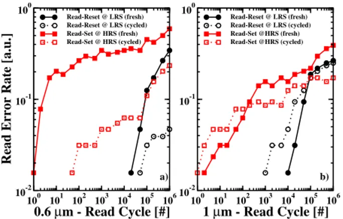
100 101 102 103 104 105 106 0.6 µm - Read Cycle [#] 0 50 100 150 200 I Read [ µ A] Read-Reset @ LRS (fresh) Read-Reset @ LRS (cycled) Read-Set @HRS (fresh) Read-Set @ HRS (cycled) 100 101 102 103 104 105 106 1 µm - Read Cycle [#] 0 50 100 150 200 Read-Reset @ LRS (fresh) Read-Reset @LRS (cycled) Read-Set @ HRS (fresh) Read-Set @ HRS (cycled) a) b)
Fig. 13. Vdd/2 pulse stress effect measured on 0.6 µm 2
(a) and 1µm2
4kbit RRAM devices (b), in both set (LRS) and reset (HRS) condition.
100 101 102 103 104 105 106 0.6 µm - Read Cycle -10 -8 -6 -4 -2 0 2 4 6 8 10 ∆ IREAD [ µ A] Read-Reset @LRS (fresh) Read-Reset @ LRS (cycled) Read-Set @ HRS (fresh) Read-Set @ HRS (cycled) 100 101 102 103 104 105 106 1µm - Read Cycle -10 -8 -6 -4 -2 0 2 4 6 8 10 Read-Reset @ LRS (fresh) Read-Reset @ LRS (cycled) Read-Set @ HRS (fresh) Read-Set @ HRS (cycled) a) b)
Fig. 14. Average read current variation measured duringVdd/2 pulse stress
measured on 0.6µm2
(a) and 1µm2
4kbit RRAM devices (b).
reset wordlines whereVRESET andVSET are the average reset
and set switching voltages, respectively. The disturb effect has been evaluated on both fresh and cycled devices, after 10k set/reset pulse operations with Vpulse = 3 V,Tpulse = 10µs.
Fig. 13 shows the average set/reset read currents and their standard deviation measured during 106 stress pulse on 0.6 µm2
(Fig. 13a) and 1µm2
(Fig. 13b) devices, for both fresh and cycled test chips. The dielectric material degradation in the MIM stack makes reset and set switching less effective, reducing the stress sensibility as well. The average current variation observed during stress is depicted in Fig. 14. The Vdd/2 stress caused a higher read current shift on fresh
devices, for both 0.6µm2
and 1µm2
4kbits RRAM devices. Ideally, considering device and circuit design margins, read resistance variation should be less than 10%. Error Correction Codes can also assist in recovery from less frequent, larger resistance fluctuations, but the occurrence of the resistance variation should be less than 1% for effective data integrity. The Read Error Rate, calculated as the fraction of cells showing a resistance variation higher than 10% duringVdd/2
stress is depicted in Fig. 15. Fresh devices show a higher error rate than cycled devices (after 10k set/reset cycles) for both 0.6µm2
and 1µm2
arrays. Although the average read current variation is higher in 1µm2
100 101 102 103 104 105 106
0.6 µm - Read Cycle [#]
10-2 10-1 100
Read Error Rate [a.u.]
Read-Reset @ LRS (fresh) Read-Reset @ LRS (cycled) Read-Set @ HRS (fresh) Read-Set @ HRS (cycled) 100 101 102 103 104 105 106 1 µm - Read Cycle [#] 10-2 10-1 100 Read-Reset @ LRS (fresh) Read-Reset @ LRS (cycled) Read-Set @HRS (fresh) Read-Set @HRS (cycled) a) b)
Fig. 15. Read Error Rate calculated on on 0.6µm2
(a) and 1µm2
4kbit RRAM devices (b). Full and dotted lines refers to fresh and cycled devices, respectively.
respect to that of 0.6µm2
devices because of a higher average set and reset currents that render the fluctuations less effective. Read disturb with set polarity stress on fresh devices in reset state is the operation that shows the highest read error rate for both 0.6µm2
(a) and 1 µm2
(b) technologies, due to the conformation of the CF.
VI. CONCLUSIONS
In this review paper it was presented a detailed electrical characterization of different RRAM arrays manufactured in a compatible BiCMOS process. The analysis was entirely focused on the reliability and performance assessment of the integrated RRAM technology, through the depiction of the major issues retrieved during the characterization. Concern-ing the formConcern-ing operation it was presented the relationship between this preliminary operation and the lifetime behavior of the array, by tackling also the typical cell-to-cell variability features. This activity lead to the search of the optimal set/reset parameters to improve the read window budget and the cycling features. Finally, the analysis of the read disturbs with their implications in advanced cross-bar architectures was evaluated showing that the integration of Error Correction Codes along with the RRAM memory is mandatory to guarantee the full data integrity.
ACKNOWLEDGEMENTS
This work was supported by the European Union’s H2020 research and innovation programme under grant agreement N◦
640073.
REFERENCES
[1] A. Chen and M. Lin, “Variability of resistive switching memories and its impact on crossbar array performance,” in IEEE Int. Reliability Physics Symposium (IRPS), 2011, pp. MY.7.1–MY.7.4.
[2] Y. Chen, B. Govoreanu, L. Goux, R. Degraeve, A. Fantini, G. Kar, D. Wouters, G. Groeseneken, J. Kittl, M. Jurczak, and L. Altimime, “Balancing set/reset pulse for>1010
endurance in hfo2/hf 1t1r bipolar
rram,” IEEE Trans. on Electron Devices, vol. 59, no. 12, pp. 3243–3249, 2012.
[3] R. Waser, Nanoelectronics and Information Technology: Advanced Elec-tronic Materials and Novel Devices. Wiley-VCH, 2012.
[4] E. Vatajelu, H. Aziza, and C. Zambelli, “Nonvolatile memories: Present and future challenges,” in Int. Design Test Symposium (IDT), 2014, pp. 61–66.
[5] D. Walczyk, T. Bertaud, M. Sowinska, M. Lukosius, M. Schubert, A. Fox, D. Wolansky, A. Scheit, M. Fraschke, G. Schoof, C. Wolf, R. Kraemer, B. Tillack, R. Korolevych, V. Stikanov, C. Wenger, T. Schroeder, and C. Walczyk, “Resistive switching behavior in tin/hfo2/ti/tin devices,” in Int. Semiconductor Conference Dresden-Grenoble (ISCDG), 2012, pp. 143–146.
[6] D. Walczyk, C. Walczyk, T. Schroeder, T. Bertaud, M. Sowiska, M. Lukosius, M. Fraschke, B. Tillack, and C. Wenger, “Resistive switching characteristics of cmos embedded hfo2-based 1t1r cells,” Microelectronic Engineering, vol. 88, no. 7, pp. 1133–1135, 2011. [7] C. Zambelli, A. Grossi, D. Walczyk, T. Bertaud, B. Tillack, T. Schroeder,
V. Stikanov, P. Olivo, and C. Walczyk, “Statistical analysis of resistive switching characteristics in ReRAM test arrays,” in IEEE Int. Conf. on Microelectronics Test Structures (ICMTS), Mar 2014, pp. 27–31. [8] N. Raghavan, A. Fantini, R. Degraeve, P. Roussel, L. Goux, B.
Govore-anu, D. Wouters, G. Groeseneken, and M. Jurczak, “Statistical insight into controlled forming and forming free stacks for HfOx RRAM,” Microelectronic Engineering, vol. 109, pp. 177 – 181, 2013.
[9] C. Chen, H. Shih, C. Wu, C. Lin, P. Chiu, S. Sheu, and F. Chen, “RRAM defect modeling and failure analysis based on march test and a novel squeeze-search scheme,” IEEE Trans. on Computers, vol. 64, no. 99, pp. 1–1, 2014.
[10] P. Lorenzi, R. Rao, and F. Irrera, “Forming kinetics in HfO2-based
RRAM cells,” IEEE Trans. on Electron Devices, vol. 60, no. 1, pp. 438–443, 2013.
[11] A. Grossi, C. Zambelli, P. Olivo, E. Miranda, V. Stikanov, T. Schroeder, C. Walczyk, and C. Wenger, “Relationship among current fluctuations during forming, cell-to-cell variability and reliability in rram arrays,” in IEEE Int. Memory Workshop (IMW), May 2015, pp. 1–4.
[12] S. Balatti, S. Ambrogio, A. Cubeta, A. Calderoni, N. Ramaswamy, and D. Ielmini, “Voltage-dependent random telegraph noise (RTN) in HfOx resistive RAM,” in IEEE Int. Reliability Physics Symposium (IRPS), June 2014, pp. MY.4.1–MY.4.6.
[13] P.-S. Chen, Y.-S. Chen, H.-Y. Lee, T.-Y. Wu, P.-Y. Gu, F. Chen, and M.-J. Tsai, “Impact of flattened TiN electrode on the memory performance of HfO2based resistive memory,” Electrochem. and Solid-State Letters,
vol. 15, no. 4, pp. H136–H139, 2012.
[14] E. Miranda, C. Walczyk, C. Wenger, and T. Schroeder, “Model for the resistive switching effect in hfo2 mim structures based on the transmission properties of narrow constrictions,” IEEE Electron Device Letters, vol. 31, no. 6, pp. 609–611, 2010.
[15] C. Zambelli, A. Grossi, P. Olivo, D. Walczyk, J. Dabrowski, B. Tillack, T. Schroeder, R. Kraemer, V. Stikanov, and C. Walczyk, “Electrical characterization of read window in ReRAM arrays under different SET/RESET cycling conditions,” in IEEE Int. Memory Workshop (IMW), May 2014, pp. 1–4.
[16] T. Iwasaki, S. Ning, and K. Takeuchi, “Stability conditioning to enhance read stability 10x in 50nm alxoy reram,” in IEEE Int. Memory Workshop (IMW), May 2013, pp. 44–47.
[17] Y.-H. Tseng, W. C. Shen, and C.-J. Lin, “Modeling of electron con-duction in contact resistive random access memory devices as random telegraph noise,” Journal of Applied Physics, vol. 111, no. 7, pp. 073 701–073 701–5, Apr 2012.
[18] W. Liu, K. L. Pey, N. Raghavan, X. Wu, M. Bosman, and T. Kauerauf, “Random telegraph noise reduction in metal gate high-k stacks by bipolar switching and the performance boosting technique,” in IEEE Int. Reliability Physics Symposium (IRPS), April 2011, pp. 3A.1.1–3A.1.8. [19] H.-Y. Lee, Y.-S. Chen, P.-S. Chen, P.-Y. Gu, Y.-Y. Hsu, W.-H. Liu, W.-S. Chen, C.-H. Tsai, F. Chen, C.-H. Lien, and M.-J. Tsai, “Comprehen-sively study of read disturb immunity and optimal read scheme for high speed hfox based rram with a ti layer,” in Int. Symp. on VLSI Technology Systems and Applications (VLSI-TSA), April 2010, pp. 132–133. [20] D. Ielmini, “Modeling the universal set/reset characteristics of bipolar
rram by field- and temperature-driven filament growth,” IEEE Trans. on Electron Devices, vol. 58, no. 12, pp. 4309–4317, Dec 2011. [21] T. Diokh, E. Le-Roux, S. Jeannot, M. Gros-Jean, P. Candelier, J. Nodin,
V. Jousseaume, L. Perniola, H. Grampeix, T. Cabout, E. Jalaguier, M. Guillermet, and B. De Salvo, “Investigation of the impact of the oxide thickness and reset conditions on disturb in hfo2-rram integrated in a 65nm cmos technology,” in IEEE Int. Reliability Physics Symposium (IRPS), April 2013, pp. 5E.4.1–5E.4.4.
![Fig. 8. Cumulative distribution of the set and reset switching voltages in the entire RRAM array [15].](https://thumb-eu.123doks.com/thumbv2/123dokorg/4701443.44817/4.892.472.818.71.295/cumulative-distribution-reset-switching-voltages-entire-rram-array.webp)