Università degli Studi di Salerno
Dipartimento di Ingegneria Elettronica e Ingegneria InformaticaDottorato di Ricerca in Ingegneria dell’Informazione IX Ciclo – Nuova Serie
T
ESI DID
OTTORATOCharacterization,
Modeling and Simulation
of 4H-SiC Power Diodes
C
ANDIDATO:
L
OREDANAFREDA
ALBANESE
T
UTOR:
P
ROF.
S
ALVATOREBELLONE
C
OORDINATORE:
P
ROF.
A
NGELOMARCELLI
Contents
Contents...I List of Figures ... III Acknowledgments...VI Abstract ...VIII Thesis Outline ...XI
Chapter 1... 1
Emerging Wide Bandgap Semiconductors Based Devices ... 1
Chapter 2... 8
Silicon Carbide (SiC)... 8
2.1 Crystallographic Structure and Polytypes of SiC... 8
2.2 Transport Properties ... 12
2.2.1 Bandgap Energy ... 16
2.2.2 Intrinsic Carrier Density... 19
2.2.3 Saturation Velocity... 21
2.2.4 Mobility ... 21
2.3 Carrier Freeze Out ... 27
2.4 Bandgap Narrowing... 31
2.5 Carrier Recombination Lifetime... 33
2.5.1 Radiative Recombination ... 34
2.5.2 Auger Recombination... 35
2.5.3 Shockley -Read-Hall (SRH) Recombination... 37
2.5.4 Effective Lifetime... 39
Chapter 3... 41
Modeling of Static Electrical Behavior of 4H-SiC pin Diodes... 41
3.1 Motivation ... 42
3.2 The I-V Analytical Model: Basic Theory ... 43
3.2.1 J-V Characteristics... 46
3.2.2 Doping and Temperature Dependencies of Physical Parameters ... 49
3.3 Model Validation... 51
3.3.2 Experimental Results... 56
Chapter 4... 64
Modeling of Dynamic Electrical Behavior of 4H-SiC pin Diodes 64 4.1 Traditional Open Circuit Voltage Decay (OCVD) Method 66 4.2 Why a New OCVD Model ... 70
4.3 A Novel OCVD Analytical Model... 71
4.3.2 Homogeneous Diffusion Equation ... 73
4.3.2 Non-Homogeneous Diffusion Equation... 74
4.4 OCVD Simulations and Model Comparison... 79
4.5 OCVD Experimental Results ... 88
4.6 RR Analysis... 92
Chapter 5... 97
Further Research Activity: Design of FPGA-based Systems ... 97
5.1 Case of Study: Context-Adaptive Variable Length (CAVLC) Encoder for Real-time Video Compression ... 98
5.1.1 Motivation ... 98
5.1.2 CAVLC Algorithm... 100
5.1.3 Proposed Design... 103
5.1.4 Synthesis and Results ... 117
Conclusions ... 121 APPENDIX A ... 123 APPENDIX B... 125 APPENDIX C ... 127 APPENDIX D ... 128 APPENDIX E... 130 Related Publications... 132 References ... 134
List of Figures
Fig. 1: Applications for power devices [2]... 1
Fig. 2: System ratings for power devices [2]... 2
Fig. 3: Johnson’s figure of merit [9] ... 4
Fig. 4: Comparison of Si and SiC power devices for power applications [2] ... 5
Fig. 5: Basic structural unit of Silicon Carbide ... 9
Fig. 6: Crystal structure of different SiC polytypes, displayed parallel to the 0 2 11 plane: a) zinkblende (cubic 3C-SiC), b) hexagonal 4H-SiC and c)hexagonal 6H-SiC [23]... 10
Fig. 7: Crystal structure of 4H-SiC polytype. Half of the atomic sites are hexagonally (h) while half are cubic (k) ... 11
Fig. 8: Maximum a) normalized breakdown voltage and b) operational temperatureof a power device realized with traditional and wide bandgap semiconductor ... 13
Fig. 9: Width (left) and resistance (right) of the drift region versus. breakdown voltage ... 14
Fig. 10: First Brillouin zone for α-SiC polytypes (left) and band-structure of 4H-SiC polytype (right)... 16
Fig. 11: Summary of the experimentally observed exciton bandgaps and their temperature variation for the different polytypes [27]... 17
Fig. 12: Linear behavior of energy bandgap as a function of percentage of hexagonal planes... 18
Fig. 13: Intrinsic carrier density as a function of reciprocal temperature... 20
Fig. 14: Schematization of the principal scattering mechanisms ... 22
Fig. 15: Electron and hole low field mobility models for 4H-SiC at To=300K... 24
Fig. 16: Temperature dependence of electron and hole low field mobility for 4H-SiC at different doping values ... 25
Fig. 17: Saturation of the electron drift velocity with increasing electric field in 4H-SiC... 27
Fig. 18: Ionization degree of Al (left) and N (right) in electro thermal equilibrium... 30
Fig. 19: Conduction and valence band displacements for 4H–SiC vs ionized doping ... 32
Fig. 20: Bandgap narrowing in 4H-SiC (left) and corresponding influence on the effective intrinsic carrier density (right) ... 32
Fig. 21: Radiative recombination process ... 34
Fig. 22: Auger recombination process ... 35
Fig. 24: Recombination lifetime in 4H-SiC as a function of the injection level
(solid curve is calculated to fit experimental data extracted from [51]) ... 39
Fig. 25: Electron and hole current components considered in the model... 44
Fig. 26: Flow chart of the static analytical model ... 48
Fig. 27: Equivalent steady-state schematic of the diode model ... 49
Fig. 28: Behaviour of the exponential term in Eqs. 3-8 vs total doping at different temperatures (from 298K to 523K), with the inclusion of the incomplete ionization effects (solid lines) or less (dashed lines)... 52
Fig. 29: JD-VD curves of devices #1 in Table 7, for two different τ0p and τ0n lifetime values, showing the effect of the bandgap narrowing and the partial activation in the terminal regions ... 54
Fig. 30: Plots of JD-VD theoretical and simulated curves at T = 373K and 473K for the device #1 in Table 7 ... 55
Fig. 31: Cross-section (left) and net doping profile (right) of the 4H-SiC samples ... 56
Fig. 32: Electron and hole concentration profiles at three distinct anode voltages for device #2 in Table 7 ... 59
Fig. 33: Comparison between JD-VD analytical and numerical curves at different temperatures for devices #2 in Table 7 ... 60
Fig. 34: Comparison between JD-VD analytical, numerical and experimental curves at different temperatures for devices #2 in Table 7 at high currents ... 60
Fig. 35: Shunting resistance detected in the I-V characteristics of the sample diode ... 61
Fig.36: ID-VD characteristics calculated by our dc model are compared with experimental and numerical data provided in [73] ... 63
Fig. 37: Test structure schematic for OCVD measurements ... 66
Fig. 38: Typical Open Circuit Voltage Decay curve... 67
Fig. 39: Typical OCVD curve at high injection levels... 69
Fig. 40: Typical voltage and lifetime transient of OCVD measurements performed at high injection levels (in t0 the current is switching-off) ... 78
Fig. 41: Comparisons between numerical simulations and model of the I-V curves... 80
Fig. 42: a) Decay of the diode voltage and b) Effective lifetime curve of devices #1SiC, #1Si and #2SiC of Table 9, switched with JD density current of 2, 20 and 20 A/cm2, respectively ... 81
Fig. 43: Transitory of the hole distribution in the epilayer of device a) #1SiC b) #2SiC and c) #1Si, for the same values of JD current of Fig. 42 (2 A/cm2 for #1SiC; 20 A/cm2 for #1Si and #2SiC)... 83
Fig. 44: Transitory of the hole current distribution in the epilayer of device a) #1SiC b) #2SiC and c) #1Si for the same values of JD current of Fig. 43 (2 A/cm2 for #1SiC; 20 A/cm2 for #1Si and #2SiC)... 84
Fig. 45: Effective lifetime curves of #1Si, for different p(x,t) approximations in the rangep(0+,t)≥NB... 85
Fig. 46: JDmax values required for a linear voltage decay, as function of WB and for different τa and
N P
S + =S + values, using the epilayer doping
NB=1014cm-3. The curves have been obtained imposing pT = pS/2 at 10
/ a
t=τ ... 86
Fig. 47: Comparison between experimental, simulated and analytical I-V curves of device #3SiC and #3Si. The inset shows the effect of a shunt resistance at lowest injection ... 89
Fig. 48: Comparison between analytical, simulated and experimental curves of a) diode voltage decay b) effective lifetime for device #3SiC, measured with a switched current JD = 10.4 A/cm2. Curves c) shows the effective lifetime measured with JD = 83 mA/cm2... 90
Fig. 49: Comparison between the analytical, simulated and experimental curves of a) diode voltage decay, b) effective lifetime, obtained for device #3Si at the injection level 0(0)/ =130 B N p ... 92
Fig. 50: Current [(a),(b)] and voltage (c) decay curves of #3SiC using IF=208A/cm2 and a) IR=5.38 A/cm2 and b) IR =58.3 A/cm2... 94
Fig. 51: Transitory of the hole distribution in the epilayer of #3SiC using IF=208A/cm2 and a) IR=5.38 A/cm2 and b) IR=58.3 A/cm2... 95
Fig. 52: Current (a) and voltage (b) decay curves of #3SiC using IF=146mA/cm2 and IR=37 mA/cm2... 96
Fig. 53: Example of the CAVLC algorithm... 101
Fig. 54: Architecture of the proposed encoder. The pre-coding and the coding stages are evidenced ... 103
Fig. 55: Block diagram of the Reorder module and the schematic of the circuitry needed for auxiliary data calculation of the i-th coefficient... 105
Fig. 56: Circuit schematic for the generation LD_TR1 and LD_NZ... 106
Fig. 57: Circuit schematic of the priority encoder. Auxiliary signal are sent to the TrailingOne module to extrapolate the second and the third trailing one positions ... 107
Fig. 58: Scheme of the TrailingOnes module ... 108
Fig. 59: Scheme of Levels module ... 109
Acknowledgments
It is anything but easy to thank all the people who contributed to my personal and professional development during my Ph.D. studies. More than anyone else, my Tutor Salvatore Bellone for his guidance and personal support throughout my doctoral study, for the privileges he gave me to work on various challenging and interesting areas. I am always impressed and inspired by his sharp insight, deep wisdom and profound knowledge.
A special thanks goes to Dr. Gian Domenico Licciardo for helping me on the device modeling work and sharing his time and comments; also, I would like to thank Professor Alfredo Rubino for his suggestions and encouragements.
I should have never started my Ph.D. studies without the support of my Department (D.I.I.I.E.), and in particular its director Maurizio Longo.
I am indebted to my colleagues at Ansaldo STS for providing a stimulating environment in which to learn and grow, and for leading me working on different exciting projects. I am especially grateful to Arturo Amendola, Fausto Del Villano, Renato De Guglielmo, Raffaele Pellecchia, Fabio Poli, Daniele Ricci, Paolo Sannino and all the boys of the development group of Naples.
Besides the above, it is my great pleasure to have this opportunity to express my gratitude to all my friends. I wish to thank my best friend Nella, for her friendly, for given me the possibility to spent together lots of memorable moments of our life. A special thanks goes to Elena, for her support, comprehension and joy she has given me in my spare time. I cannot forget Maria Domenica: she is a beautiful and unannounced gift of these years sent at the university.
Then, I am especially indebted to my family for their encouragement and for putting up with my crazy working hours. My wonderful mother, who teach me the importance of the Life, in each
its aspect. My dear Father, who teach me that the Love goes also besides the life itself. I am grateful to my aunt Gemma and my uncle Gerardo, who give me an incomparable love and support in every important moment. I want to remember my uncles Gino and Alfonso, who give me the perception of a solid family.
Last but certainly not least, a very special thanks to Paolo, who made this thesis possible by his support and unrivalled Love.
Thank you to everyone, Lory
Abstract
Exploring the attractive electrical properties of the Silicon Carbide (SiC) for power devices, the characterization and the analysis of 4H-SiC pin diodes is the main topic of this Ph.D. document. In particular, the thesis concerns the development of an auto consistent, analytical, physics based model, created for accurately replicating the power diodes behavior, including both on-state and transient conditions. At the present, the fabrication of SiC devices with the given performances is not completely obvious because of the lack of knowledge still existing in the physical properties of the material, especially of those related to carrier transport and of their dependences on process parameters. Among these, one can cite the degree of doping activation, the carrier lifetime into epitaxial layers that will be employed and the sensitivity of some physical parameters to temperature changes. Therefore, a set of investigative tools, designed especially for SiC devices, cannot be regarded as secondary objective. It will be useful both for process monitoring, becoming essential to the tuning of technological processes used for the implementation of the final devices, and for a proper diagnostics of the realized devices. Following this need, in our research activity firstly a predictive, static analytical model, including temperature dependence, is developed. It is able to explain the carrier transport in diffused regions as function of the injection level and turns also useful for better understanding the influence of physical parameters, which depend in a significant way from the processed material, on device performances. The model solves the continuity equation in double carrier conditions, taking into account the effects due to varying doping profile of the junction, the spatial dependence of physical parameters on both doping and injection level and the modification of the electric field of the region with the injection regime. The model includes also the device characterization at high temperatures to analyze the influence of
thermal issues on the overall behavior up to temperature of 250°C. The accuracy of the static model has been extensively demonstrated by numerous comparisons with numerical results obtained by the SILVACO commercial simulator.
Secondly, with the aim to properly account for the dynamic electrical behavior of a diode with generic structure, the static model has been incorporated in a more general, self-consistent model, allowing the analysis of the device behavior when it is switched from an arbitrary forward-bias condition. In particular, the attention is focused on an abrupt variation of diode voltage due to an instantaneous interruption of the conduction current: although this situation is notably interesting for the study of the switching behavior of diodes, the voltage transitory is also traditionally used in different techniques of investigation to extract more information about the mean carrier lifetime. This occurs, for example, in the conventional Open Circuit Voltage Decay (OCVD) technique, where the voltage decay due to the current interruption is useful for an indirect measure of minority carrier lifetime in the epitaxial layer.
Because of its heavy dependence on processes, the carrier lifetime is an important parameter to be monitored, especially in the case of bipolar devices, and it cannot be neglected. Due to the existent uncertainty about this parameter in SiC epi-layers, the OCVD method reveals itself a practical way to overcoming this limit.
In detail, by using our self-consistent model, that exploits an improved method of the traditional OCVD technique, it is possible to characterize the carrier lifetime into 4H-SiC epitaxial layer of a generic diode under test, obtaining the spatial distributions of the minority carrier concentration and carrier lifetime at any injection regime. The overall model performances are compared to both device simulations and experimental results performed on Si and 4H-SiC rectifier structures with various physical and electrical characteristics. From the comparisons, the model results to have good predictive capabilities for describing the spatial–temporal variation of carriers and currents along the whole epi-layer, proving contextually the validity of the used approximations and allowing also to resolve some ambiguities reported in the literature, such as the stated inapplicability of the OCVD method on thick epitaxial layers, the reasons of the
observed non linear decay of the voltage with time, and the effects of junction properties on voltage transient.
Finally, with the imposition of right boundary conditions, it is possible to use the versatility of the developed model for extending the analysis and obtaining a physical insight of any arbitrary switching condition of 4H-SiC power diodes.
Thesis Outline
The thesis is arranged with a general introduction in chapter 1 to the potentiality of wide bandgap semiconductors, such as Gallium Nitride (GaN) and Silicon Carbide (SiC), as attractive materials in the electronic field. At this time, the state of the semiconductor industry is presented to give evidence of how these emerging technologies are expected to shift the theoretical limits for electronic devices even far beyond those of the most advanced Silicon devices.
The second chapter describes the set of electrical and physical characteristics which have relevance to the analysis of power diodes in Silicon Carbide. The attention is focused on the 4H-SiC polytype, because of its superior electrical properties with respect to the others. Along with a brief excursus on the physical models which are today available for this material, the analytical expressions to describe the transport and physical parameters, such as minority carrier lifetimes, mobility, bandgap narrowing and incomplete ionization effects, are also introduced. In order to obtain a suitable description of the main physical phenomenon associated to Silicon Carbide, some of these models were incorporated in our diode model and implemented in the numerical simulator.
Chapters 3 and 4 describe, respectively, the analytical development of our static and dynamic model. Here, with the aim to better highlight the versatility of the resultant auto-consistent model in the investigation of 4H-SiC power diodes with arbitrary structures, comparisons with the numerical and experimental data are presented. The usefulness of the model to predict the electrical behavior of a generic diode is proven at the end of Chapter 4, where the analysis has been extended to other switching conditions, such as reverse recovery transients.
In the last chapter a further research activity is finally presented. It is focused on the design of a new Context-Adaptive Variable Length Coding (CAVLC) encoder architecture, particularly aimed to be implemented with Field Programmable Logics (FPLs) like FPGAs.
Chapter 1
Emerging Wide Bandgap
Semiconductors Based Devices
In the last six decades Silicon technology has always dominated the power electronic field, providing semiconductor devices able to operate in a broad spectrum of power levels and frequencies. In detail, as shown in Fig. 1, thyristors are favored for the low frequency and high power applications, IGBTs for the medium frequency and power applications, and MOSFETs are typically restricted to lower power and higher frequency applications [1]. Therefore, Silicon devices are
Fig. 2: System ratings for power devices [2]
presently able to serve every type of power application, each characterized by own current and voltage ratings as displayed in Fig. 2, including variable speed motion control, electric vehicle drives, uninterruptible power supplies (UPS), until to the higher power distribution, transmission and traction markets. However, with the aim to guarantee a continue improvement of power systems, the required performance by future devices is destined to increase continuously, so that the theoretical limits related to the devices based on traditional technologies are rapidly approaching. For overcoming the problem, which will make the conventional semiconductors incompetent for potential demands, especially in high power and high efficiency applications, manufacturers are exploring the possibilities of using valid counterparts. Among these, favourite candidates are the wide band gap semiconductors, like Gallium Nitride (GaN) and Silicon Carbide (SiC): compared to Silicon, they exhibit largely better figures for most of the key specifications, such as energy gap, electric field, electron mobility, and melting point, offering intrinsically better performance in terms of breakdown voltage, switching frequency and system efficiency. Thus, these innovative materials, due to their
unique electrical and chemical properties, are becoming very attractive into the electronics field.
At the present, for its direct band-to-band transition, GaN results superior to SiC for optical applications, favouring a well implanted and widely diffused semiconductor technology for ultra-bright blue light emitting diodes and lasers, ultraviolet emitters, and optical detectors [3]. Besides, the high critical field of both GaN and SiC gives a further advantage to these materials compared to Si and GaAs for RF power devices. In particular, SiC shows higher electron mobility than Si but GaN’s electron mobility is higher than SiC, so that GaN is the best candidate material for very high frequencies. In this perspective, in the last decades, GaN based devices have been developed for RF wireless applications where they can efficiently replace Silicon transistors [4]. The spread in this field has also opened the doors to the power switching capability in the lower frequency range and thus also in the power electronic applications. Despite owing fundamentally superior electronic properties with respect to SiC, however, GaN must overcome the lack of a native substrate excluding any vertical devices, so that GaN based devices are usually characterized by lateral configurations on Si or SiC substrates. Regardless of the type of application, in the switching or RF field, the most extensively used lateral structure is becoming the High Electron Mobility Transistor (HEMT) [5]. The primary adopters of GaN on SiC HEMTs are defence systems, where performance is paramount and the cost is not the primary factor. Actually, GaN on SiC HEMTs are emerging for use at very high frequencies such as C, X and Ku bands, bringing to the integration of communications systems and multiple radars into a single amplifier [6-7]. Besides, RF GaN on SiC HEMTs are also manufactured [8] to replace the incumbent Si Laterally Diffused MOS (LDMOS) devices and the Pseudomorphic HEMTs (PHEMTs) of Gallium Arsenide, which are extensively used in telecommunication market. For example, since the base stations for Mobile Worldwide Interoperability for Microwave Access (WiMAX) require high power efficiency to drastically reduce the increase of power consumption, high-efficient transmission amplifiers are needed.
Fig. 3: Johnson’s figure of merit [9]
In order to make possible the development of low compact base stations that offer both simple implementation and low operation cost, currently power amplifiers can be realized with GaN HEMTs. As displayed in Fig. 3, in fact, they are characterized by higher breakdown voltage with higher cut-off frequency than devices based on other materials (such as LDMOS and PHEMTs), providing in this way more system efficiency [9]. Finally, although GaN on Si HEMTs are not as performing as the equivalent SiC based device, they are beginning to dominate cost-driven sectors, thanks to their discrete results along with their lower cost.
On the other side, for applications characterized by high temperatures and harsh environments, SiC based devices are indeed favoured to operate at higher power densities than either GaN or Si. This is due to SiC’s thermal conductivity, whose high value permits to the material of conducting heat more efficiently. So that, while actual Silicon transistors reach their normal operational temperatures approximately at 125°C, becoming highly susceptible to harsh environments, equivalent SiC devices promise to operate at temperature up to 600°C, and also at high power densities for both
Fig. 4: Comparison of Si and SiC power devices for power applications [2]
medium and high frequency switching applications [10-11]. Therefore, higher thermal conductivity, combined with wide bandgap and high critical field, gives to SiC technology an advantage when high power is a desirable device feature [12-13]. Besides, compared to hetero-epitaxial GaN devices, SiC based structures are expected to dominate in power applications, also for a lower cost and easier fabrication of defect free wafers. This is due to important developments obtained in the last decades on sublimation process for the growth of Silicon Carbide crystals [14-15] and the commercial availability of single crystal 6H- and 4H-SiC wafers [16].
As shown in Fig. 4, the hope is that Silicon Carbide will enable a significant advance in the state of the power electronics in terms of ratings, losses, and speed of operation, shifting the theoretical limits for electronic devices even far beyond those of the most advanced Si devices.
Focusing on the determining factors in the operating frequency of a power circuit, such as the parasitic or non-idealities effects of the active devices, at the present the optimization effort on Silicon-based power devices has brought to just discrete improvements of performances. For majority carrier devices, for instance MOSFETs or JFETs, the limiting parasitic factors are the conduction resistance
(which determines conduction loss) and device capacitances (whose charging and discharging during turn-on and turn-off lead to switching loss). In a similar manner, for minority carrier devices, such as bipolar transistors and IGBTs, the conduction loss is due to both junction voltage drops and conduction resistance, while the switching behavior brings to further loss. Actually, regarding to Si MOSFET switching times, a decrease from 1.2µs down to 100ns is obtained; similarly, about the switching time of Si IGBTs, particularly the turn-off time, it has decreased from 3µs to 1.2µs. In terms of overall device ratings, the state of the power semiconductor industry at this time is power MOSFETs at 600V and 20A, and IGBTs up to 6kV and 1200A.
Regarding to Silicon Carbide market, Cree [16] is the leading manufacturer of SiC-based diodes for power control and management: its family of Zero Recovery rectifiers has essentially no reverse recovery at 600V, 650V and 1200V breakdown and is targeted for applications where low switching loss is required. More recent batches have achieved leakage currents of 18µA at 25°C and 50µA at 200°C with 1200V reverse bias. The offered current ratings range from 1A÷20A at 600V to 5A÷20A at 1200V. Rectifiers with currents of 10A and 25A at 1700V are also available in chip form. Other different companies sell Schottky diodes up to 20A [17], such as SiCED, Infineon and Rockwell Scientific.
For higher voltage applications it is necessary to use a pin device structure: actually, 20kV devices have been build in standard 200µm epi-layers. Respect to a SiC Schottky diode, it is observed that the conduction drop of a pin diode of equivalent area is lower at sufficiently high currents.
SiC MOSFETs developed by Cree were achieved by paralleling 3, 1.6mm x 1.6mm, dices. It is interesting to observe that the resulting SiC MOSFET achieves approximately 1/30th of the on-state resistance of an equivalent Si based MOSFET in the same die area. However, it is also important to note that the SiC MOSFET has a higher device capacitance or total drain charge than the corresponding Si device: given the thinner intrinsic region, the capacitance per unit area is approximately 10 times higher.
The reliability of the oxide remains the major concern to face for a commercial employment of SiC MOSFETs. The native oxide of
Silicon Carbide is SiO2, which is typically grown on the SiC wafer
using chemical vapour deposition (CVD) in a Silane (SiH4) and
oxygen environment. The problems occur at the SiO2–SiC interface,
where some of the Si is absorbed into the oxide layer, leaving behind carbon atoms that granulate and form carbon clusters at the interface. The resultant oxide layer is typically thicker than a corresponding Si device, requiring higher electric field to achieve channel inversion. Recent measurements show that the field strength in the gate oxide of these high voltage MOSFETs is too high for reliable operation at elevated temperatures. The simplest solution is to fabricate the devices with a thinner gate oxide: however, this requires an improvement of the quality of both oxide and interface.
From the above considerations, it is clear that SiC technology is not mature enough in order to benefit a high volume of production [18-19] in the field of power electronics. Much work must be done in this direction, especially for still unresolved material science issues. Many of the physical and electronic properties of SiC, in fact, are less well known than for Si and more commonly used III-V compounds. Among these, minority carrier lifetime, an important parameter specially for bipolar devices, is not still completely understood: although some measurements have been made on representative SiC material, its value on typical grown layers is not generally well evaluated and more attention is needed in this area. Due to the lake of a mature knowledge of their behavior, at the present, the majority of SiC devices are only experimental elements, with the exception of Schottky diodes, which are available for rectifier market.
Nowadays many companies and industry centers are devoting efforts to study and develop SiC devices, relying on the impact and benefits that this technology could have on the design of future power systems. With this aim, device optimizations are traditionally performed by hand, changing device parameters until sufficient performance is achieved. This is very time consuming work without any guarantee of achieving an optimal result.
Our developed analytical model, presented in the following, results a valid tool for evaluating the effect of geometrical and electrical changes on overall performance of 4H-SiC power diodes.
Chapter 2
Silicon Carbide (SiC)
Due to a rigorous formalism, the proposed model shows a good ability to support a large number of physical models, such as carrier mobility, incomplete ionization of doping atoms, and lifetime profiles. In this chapter, after a brief introduction to the principal structural characteristics of Silicon Carbide, the attention is focused on the physical and electrical parameters useful for analyzing the behavior of power diodes realized with this semiconductor, especially with the polytype of interest, the 4H-SiC.
2.1 Crystallographic Structure and Polytypes of
SiC
The Silicon Carbide is the most stable compound of carbon (C) and silicon (Si) among those belonging to IV group of periodic table, with a partially ionic bond between C and Si atoms. The fundamental structural unit is a tetrahedron, with four atoms of Si (C) and one atom of C (Si) at the center, as shown in Fig. 5.
Fig. 5: Basic structural unit of Silicon Carbide
The distance named a between adjacent Si and C atoms is near to 3.08 Å; the C atom is located at mass centre of the tetraedric structure so that to keep an equidistance among neighbouring Si atoms of about
= 8 3
a 1.89 Å. The height of the cell, named c, changes among the polytypes: in particular, the c/a ratio is 1.641, 3.271 e 4.908, respectively for 2H-, 4H- and 6H-SiC [20].
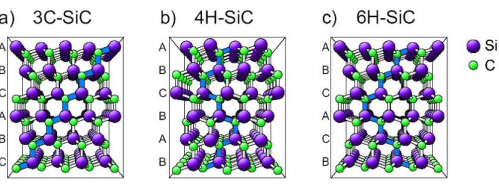
Silicon Carbide exhibits a one-dimensional polymorphism called polytypism. There are a large number of different SiC polytypes which are characterized by the stacking sequence of the tetrahedrally bonded Si-C bilayers. While the individual bond lengths and local atomic environments are nearly identical, the overall symmetry of the crystal is determined by the stacking periodicity [21]. There are three possible positions available for each SiC bilayer with respect to its adjacent bilayers: all maintain the tetrahedral bonding scheme of the crystal and to each one it is arbitrarily assigned the notation A, B, or C. A schematic view of different stacking sequence for some common SiC polytypes is presented in Fig. 6, while a complete analysis to SiC polytypism can be found in [22].
Fig. 6: Crystal structure of different SiC polytypes, displayed parallel to the 1120
plane: a) zinkblende (cubic 3C-SiC), b) hexagonal 4H-SiC and c) hexagonal 6H-SiC [23]
Depending on the stacking order, the bonding between Si and C atoms in adjacent bilayer planes is either of zinkblende (cubic) or wurtzite (hexagonal) nature. So that each type of bond provides a slightly altered atomic environment, whose effect is relevant when the substitutional impurity incorporation and electronic transport properties of SiC are considered. In Fig. 7, the inequivalent layers are denoted by the letters h and k and the hexagonality of a polytype can be defined as the percentage of h-type layers, according to the Jagodzinski’s notation [24].
There are other different ways to indicate the SiC polytypes. The traditional notation consists of using the stacking sequence, so that 4H- and 6H-SiC are respectively indicated by the sequence of ABCB and ABCACB. Besides this, another commonly used notation is due to
Fig. 7: Crystal structure of 4H-SiC polytype. Half of the atomic sites are
hexagonally (h) while half are cubic (k)
Ramsdell [25], who categorizes every polytype with a number, followed by a letter: the first one represents the stacking periodicity, while the latter the bonding type, so that 4H- and 6H-SiC are hexagonal polytypes (which are also referred to as α-SiC in literature) with a stacking period of four and six, respectively. A review of the possible notations for indicating the principal SiC polytypes is reported in Table 1.
Ramsdell ABC Jagodzinski
2H (wurtzite) AB h 3C (zinkblende) ABC k
4H ABCB hk
6H ABCACB hkk
15R ABCACBCABACABCB hkkhk Table 1: The most common notations of some of the SiC polytypes [26]
2.2 Transport Properties
The transport properties of 4H-SiC polytype are listed in Table 2, along with other wide bandgap semiconductors, like Gallium Nitride and Diamond, and the most commonly used semiconductor materials (Si and GaAs). By a direct comparison, the advantages of SiC over Si are the tenfold increase in breakdown fields, twofold increase in saturation velocity, and more than doubling of thermal conductivity. Although the carrier mobility in Silicon Carbide is somewhat lower than in Silicon, in general the transport parameters give Silicon Carbide devices better performances than comparable Silicon devices. Investigating the basic electrical and physical parameters for electronic devices, such as bandgap (Eg), mobility (µ), saturation velocity (vsat), breakdown electric field (Ecrit), and thermal conductivity (λ), it instantly evident that wide bandgap semiconductors are very promising materials for using in high performance electronic devices.
Si GaAs 4H-SiC GaN Diamond Eg@300K [eV] 1.1 1.4 3.2 3.4 5.45 Ec [MV/cm] 0.3 0.4 2.2 2.0 10 sat v [x107 cm/s] 1.0 2.0 2.0 2.5 2.7 3 16 10 @N= cm− n µ [cm2/V s] 1500 8500 720 1000 2200 3 16 10 @N= cm− p µ [cm2/V s] 480 400 120 30 850 r ε 11.9 13.1 9.7 8.9 5.5 λ [W/cm K] 1.5 0.5 5 1.3 22 Table 2: Key characteristics of SiC vs. other semiconductor materials
Fig. 8: Maximum a) normalized breakdown voltage and b) operational temperature
of a power device realized with traditional and wide bandgap semiconductor
In fact:
• A higher electric breakdown field brings to power devices with higher breakdown voltages, as shown in Fig. 8.a, where the reported values are normalized to the breakdown voltage of Si diode, together with the assumption that the diodes are realized with the same doping density. As can be seen, the theoretical breakdown voltage of a Diamond diode results in 500 times bigger than of a Si diode, while the breakdown voltage numbers for 4H-SiC and GaN are 46 and 34 times that of Si diode, respectively. For the same breakdown voltage, instead, the consequence of higher Ecrit is the reduction of the width of the drift region, which enables smaller unipolar device and smaller on-resistance as can be seen in Fig. 9. This turns in lower conduction loss and in a consequent increasing of the efficiency.
Fig. 9: Width (left) and resistance (right) of the drift region vs. breakdown voltage
• Semiconductors with wider bandgap can operate at higher temperatures (see Fig. 7.b).
• Due to the direct proportionality between the high frequency switching capability of a semiconductor material and its drift velocity, it is expected that wide bandgap materials, having more than twice the drift velocity of Si, could be switched at higher frequencies than their Si counterparts. Moreover, higher drift velocity allows charge in the depletion region of a diode to be removed faster, so it is likely that the reverse recovery current of diodes based on wide bandgap semiconductors is smaller and the reverse recovery time is shorter.
• The thermal conductivity does not directly affect the performance, but with a good thermal conductivity it is easier to conduct the heat away from the chip to a heat sink, so it obviates the need to have bulky and expensive cooling systems.
As discussed in Chapter 1, all these properties make wide bandgap semiconductors good candidates for high power, high temperature, and high frequency devices. However, it is important to remark that, respect to the other wide bandgap competitors, SiC is the best suitable transition material for future power electronics devices. In fact, although Diamond is the material with the best electrical characteristics, it must face significant processing hurdles that must be overcome before it can be commercially used for power applications. On the other side, GaN turns out less attractive than SiC for different aspects, such as the unavailability of pure wafers, the lake of a native oxide required for MOS device, and for having a thermal conductivity equals only one-fourth of that of SiC. However, it must be remarked that, although SiC process technology is continuously improving, it is not yet mature to introduce large volume of commercial devices into the market. In fact, compared to Silicon, this innovative material remains very expensive, the obtained wafers are just of discrete quality and the resultant devices show electrical behaviors not completely known.
2.2.1 Bandgap Energy
Many of the favourable transport parameters in SiC are related to its large bandgap: along with conduction and valence band structure, it defines the electric properties of the semiconductor. Band structure calculations for SiC have been made for the past forty years; early, the theorists have concentrated on the zinkblende 3C-SiC polytype and the wurtzite 2H-SiC structure given that the other polytypes are much more complicated due to their larger unit cell [27]. Then, since both 3C-SiC and 2H-SiC are indirect-gap semiconductors, they have reasonably assumed that all polytypes are indirect-gap semiconductors. In the following years, the accuracy of initial calculations has been considerably improved to work also on the band structures of 4H- and 6H-SiC polytypes [28-30]. The resultant first Brillouin zone and band-structure for 4H-SiC are shown in Fig. 10 (the hexagonal direction [0001] coincides with the kz axis). In a
similar manner respect to the other polytypes, the top of valence band for 4H-SiC is localized at the Γ–point, while the bottom of conduction band is localized in the M–point.
Fig. 10: First Brillouin zone for α-SiC polytypes (left) and band-structure of 4H-SiC
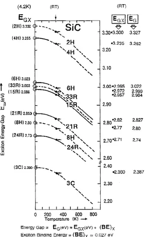
Fig. 11: Summary of the experimentally observed exciton bandgaps and their
temperature variation for the different polytypes [27]
Fig. 11 summarizes the experimentally observed exciton bandgaps and their temperature variations. Experiments have also given an estimate of the bending energy of the exciton 3C-SiC of about 27meV: with the assumption that this value is not different for the other polytypes, the actual bandgap can be calculated by adding an amount of 27meV to the known value of the exciton bandgap. Ambient-temperature values of total (EG) and exicton (EGX) bandgap
Fig. 12: Linear behavior of energy bandgap as a function of percentage of hexagonal
planes
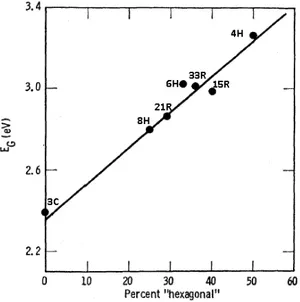
Choyke, Hamilton and Patrick in [31] have derived an empirical correlation of EG with percentage of hexagonal planes, whose value
can be easily obtained by Jagodzinski’s notation (see Table 1): for the principal polytypes, a plot of energy gap against percent hexagonal is shown in Fig. 12, evidencing a quasi linear relationship.
Due to a wide bandgap for all SiC polytypes, ranging from 2.38eV to 3.33eV (see Fig. 11), it is evident that electronic devices in Silicon Carbide can operate at extremely high temperatures without suffering from intrinsic conduction effects, since they are negligible at temperatures up to 600°C. Moreover, being the bandgap the minimum energy required to create an electron-hole pair, SiC reveals suitable as a detector material for UV radiation with minimal noise from the visible background [32], since the value of about 3eV as bandgap energy corresponds to a photon with wavelength approximately of 400nm, making SiC an insensible material to the main part of the visible spectrum.
Because of the interest for the employment of SiC material also for high temperature applications, it is relevant to adequately describe
the dependence of bandgap energy by this parameter. Pioneering work in this area was performed by Choyke [33] who observed that, in the temperature range 0÷800 K, the bandgap value can be evaluated by an analogue expression used for Silicon. Although Choyke’s measurements are dated, at the present it is been observed that they accurately predict, for all α-SiC polytypes, the temperature variation of the bandgap. This results equal to dEg/dT=-3.3x10-4 eV/K, so that the complete bandgap relation for a generic SiC polytype, with a total bandgap at ambient temperature (TO) equals to EG, is given by the
following: Eg(T)= EgO +α(T −TO), with ⎪ ⎪ ⎩ ⎪⎪ ⎨ ⎧ = − = = − ] [ 300 ] / [ 10 3 . 3 ] [ E 4 G K T K eV eV E O gO α (2-1)
2.2.2 Intrinsic Carrier Density
With the parabolic approximation for conduction and valence band [34], the intrinsic carrier concentration can be expressed as a function of the temperature: KT T E V C i g
e
T
N
T
N
T
n
2 ) ()
(
)
(
)
(
=
− (2-2) where K is Boltzmann constant andNC( )
T and NV( )
T are the effective density of states in the conduction and valence band, respectively, which are given by:
( )
2 3 2 3 2 * ) ( 2 2 ⎟⎟ ⎠ ⎞ ⎜⎜ ⎝ ⎛ = ⎟⎟ ⎠ ⎞ ⎜⎜ ⎝ ⎛ = O O C e c C T T T N h KT m M T N π (2-3a)Fig. 13: Intrinsic carrier density as a function of reciprocal temperature
( )
2 3 2 3 2 * ) ( 2 2 ⎟⎟ ⎠ ⎞ ⎜⎜ ⎝ ⎛ = ⎟⎟ ⎠ ⎞ ⎜⎜ ⎝ ⎛ = O O V h V T T T N h KT m T N π (2-3b) with * e m and * hm the electron and hole effective masses, and Mc the equivalent valleys in conduction band. For the 4H-SiC polytype, the values of these parameters are: *
e
m =0.77m0 [35], m =1.2m*h 0 [36] (where m0 is the electron rest mass) and Mc=3.
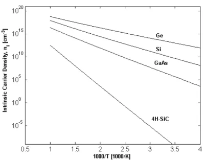
Fig. 13 shows the intrinsic carrier concentration for traditional and wide bandgap semiconductors, where also the temperature dependence of energy gap is considered. As expected, the bigger bandgap brings to lower value of ni: in particular for 4H-SiC, at
ambient temperature the intrinsic carrier density results smaller by the order of 18 compared to Silicon.
The modification of the density of states by heavy doping leads to an additional influence on intrinsic carrier density, the so-called “bandgap narrowing”. This phenomenon, in more detail analyzed in
section 2.4, is generally modelled by rigid shifts of the band edges [37] and brings, evaluating the consequent bandgap shrinking by the term ∆Eg, to express the effective intrinsic carrier concentration as:
n
ien
ie
2KT Eg ∆=
(2-4)2.2.3 Saturation Velocity
At high electric fields the velocity ceases to be proportional to the electric field, due to increased scattering and it saturates at vsat value, which for SiC is approximately twice the value for silicon; in this way, it is allowed to realize faster devices with shorter switching times.
2.2.4 Mobility
As shown in Table 2, the mobility in SiC is somewhat lower than for Silicon and much lower than in high-mobility materials, such as GaAs: however, the low mobility in SiC devices is compensated by operation at larger electric fields taking advantage of the higher carrier velocity.
The mobility describes the mean velocity of electrons and holes when an electric field is applied. At low electric fields, the velocity increases proportional to the field, since the carrier mobility is fundamentally due to the Coulomb and phonon scattering; for higher fields, the proportionality is lost and the velocity saturates at vsat. In general, there are various scattering mechanisms, schematized in Fig. 14, which determine the free carrier mobilities.
Fig. 14: Schematization of the principal scattering mechanisms
Due to the complex nature of these mechanisms, phenomenological models have been developed for the various experimentally observed mobility phenomena in Si devices [38]. The contributions from different scattering processes can be combined using the simple Matthiessen’s rule:
=
∑
i i eff µ µ 1 1 . (2-5)In literature, a lot of low field mobility models for Si are available: they represent, along with experimental data and Monte Carlo simulations published for SiC, a valid fundament to develop empirical expressions related to the mobility for this innovative material. Contributions focused on this aim are [39-30], while a comparative analysis of these models can be found in [41].
Because of their crystallographic structure, the α-SiC polytype are characterized by an anisotropy of the principal electro thermal parameters. Although, in general, anisotropic parameters result expressed by second rank tensors, for 4H- and 6H- polytypes they are reduced to a diagonal form [42], so that it is possible to use the following convenient representation for the electron mobility:
⎥ ⎥ ⎥ ⎥ ⎥ ⎥ ⎦ ⎤ ⎢ ⎢ ⎢ ⎢ ⎢ ⎢ ⎣ ⎡ = ⊥ ⊥ || 0 0 0 0 0 0 µ µ µ µ .
Actually an exhaustive modelling of anisotropic properties does not exist; since the most of SiC devices are realized on wafers with surface orthogonal, or lightly rotated, to c-axis ([0001] direction), it is common rule to define an anisotropic ratio between base-plane and the [0001] direction. Following this observation, because the commonly measured mobility is orthogonal to c-axis (µ┴) while the parallel component is generally not equal, the ratio between these components is derived by experiments or by Monte Carlo simulations.
In relation to 4H-SiC, the obtained results define a unitary ratio and a ratio of µ┴/µ||=0.8 for holes and electrons, respectively. Anyway, due to a better isotropic behavior of 4H-SiC respect to the other polytypes, it is possible to consider just the mobility in the base-plane with a reasonable approximation.
From published experimental data obtained by Hall measurements on 4H-SiC bulk epitaxial layers, free carrier mobility tensor components are extracted, within a wide range of impurity concentration and temperature [39-43]. The data can be well described using the phenomenological model of Caughey-Thomas [44],
including the temperature dependence for T > 300K:
i i i i i T N N T T T N T crit i i i i low i δ γ α β α µ µ µ µ ⎟ ⎠ ⎞ ⎜ ⎝ ⎛ ⎟⎟ ⎠ ⎞ ⎜⎜ ⎝ ⎛ + ⎟ ⎠ ⎞ ⎜ ⎝ ⎛ − ⎟ ⎠ ⎞ ⎜ ⎝ ⎛ + ⎟ ⎠ ⎞ ⎜ ⎝ ⎛ = 300 1 300 300 300 ) , ( min 0 max 0 min 0 , i=n, p (2-6)
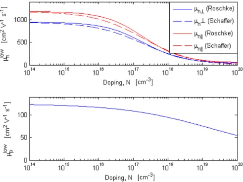
where the various parameters Ncrit, α, β, γ and δ, taken from the
measurement results of Roschke et al. and Schaffer for SiC, are listed in Table 3. Although the mobility parameters depend on technology,
max 0i µ (TO) [cm2/V s] min 0i µ (TO) [cm2/V s] crit i N [cm-3] αi βi δi γi n 950 40.0 2.00E17 -2.40 0.76 -0.76 p 125 15.9 1.76E17 -0.5 -2.15 0.34 -0.34
Table 3:Values of low field mobility parameters for 4H-SiC, at To=300K
this table can serve as a base for evaluating measured device characteristics. In Fig. 15 it is interesting observe that, for the same doping, the less value of hole mobility compared with electron one is related to a smaller electron effective mass. The temperature dependence of electron and hole mobility is shown in Fig. 16.
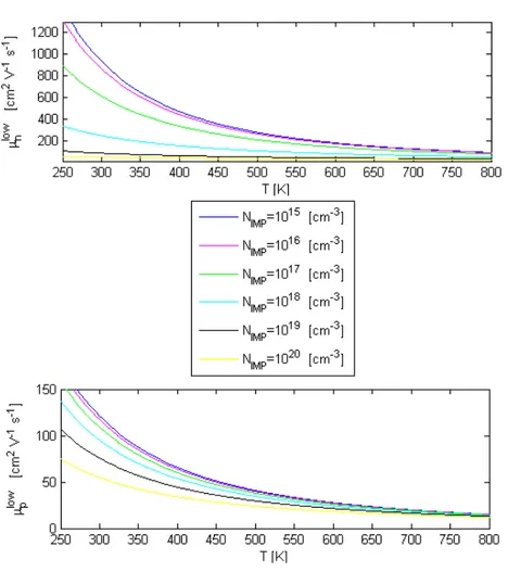
Fig. 16: Temperature dependence of electron and hole low field mobility for 4H-SiC
at different doping values
At high electric field, the mobility models must keep in count their dependence from it; for SiC, the analytical expression used for this aim is analogue to that largely employed for Silicon [39]:
β β µ µ µ 1 1 ⎥ ⎥ ⎦ ⎤ ⎢ ⎢ ⎣ ⎡ ⎟⎟ ⎠ ⎞ ⎜⎜ ⎝ ⎛ + = sat low i low i i v E , i=n, p. (2-7a)
with the temperature dependence of vsat and β coefficient described by the following:
⎪ ⎪ ⎩ ⎪ ⎪ ⎨ ⎧ + = + = − b T T o T sat ref e a e v v
β
β
600 max 6 . 0 1.
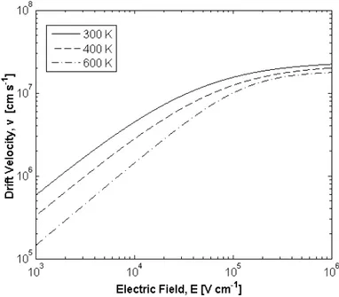
(2-7b)All available measured data refers to a current flow perpendicular to the c-axis, while no measured data of holes is presently available. For 4H-SiC the saturation velocity is 2x107cm/s at ambient temperature and the different fitting parameters (vmax, βo, a, Tref e b) are summarized in Table 4.
In Fig. 17 is plotted the electron drift velocity as a function of electric field in 4H-SiC at three different temperature and with a doping of 1017cm-3.
vmax [cm/s] βo Tref [K] a b
4H-SiC 4.77E7 0.816 327 4.27E-2 98.4
Fig. 17: Saturation of the electron drift velocity with increasing electric field in
4H-SiC
2.3 Carrier Freeze Out
Although the large bandgap of SiC is a favourable property in most cases, it also causes one of its largest disadvantage: the energy levels for the doping materials used in Silicon Carbide are located at a significant distance from the band-edge. This brings to a high thermal ionization energy also at ambient temperature, comparable value to the mean thermal energy for the carriers at this temperature (KT=25.9meV). The resultant effect is that a fraction of the carriers are not thermally activated: they are instead frozen in the band-gap without being ionized. This phenomenon is known as freeze-out and in the traditional semiconductors is significant at low temperatures. With the aim to accurately describe the doping phenomenon, it must keep in count that the inequivalent α-SiC sites (one with cubic
surrounding and the other with hexagonal surrounding) are expected to cause also site dependent impurity levels [45].
Generally, the most common dopants for 4H- and 6H-SiC are nitrogen (N) and phosphor (P) for n-type layers, while aluminum (Al) and boron (B) are acceptor atoms. In detail, N preferentially incorporates into the lattice sites which are normally occupied by C atoms, while P and Al prefer the Silicon sites of SiC and B may substitute on both sites [46].
Relatively to the behavior of bipolar devices, the incomplete ionization of the most common dopants in SiC will affect it within a wide range of operation conditions; fundamentally, it will causes a substantial increase of the bulk resistance dependent on temperature and doping concentration. Therefore, an appropriate incomplete ionization model which accounts for variation of ionization rates and also the lattice site-dependent impurity level must be considered. By referring to a generic n-type extrinsic region, because a corresponding equation it can be derived for the holes, the relative position of the Fermi level, E , required in the ionized (activated) Fn donor density formula:
1 1 exp Fn d D D d E E N N g KT − + = ⎡ + ⎛ − ⎞⎤ ⎜ ⎟ ⎢ ⎝ ⎠⎥ ⎣ ⎦ (2-8)
can be evaluated by equating the above expression with the majority carrier density: 1.5 ( ) exp C Fn C O O E E T n N T T KT ⎛ ⎞ ⎛ − ⎞ = ⎜ ⎟ ⎜− ⎟ ⎝ ⎠ ⎝ ⎠ (2-9) being g the degeneration factor of conduction band, thus obtaining d the following expression for the ionization grade:
KT E C D d KT E C D d D D D d d e T N N g e T N N g N N ∆ ∆ + − + + = = ) ( 2 ) ( 4 1 1 ξ (2-10)
where ND is the doping level, ∆Ed represents the energy distance of donor level from conduction band, and NC(T) is the effective density of states presented in the subsection 2.2.2.
In the case of multiple, site-dependent energy levels, the ∆Ed expression becomes: ⎪⎩ ⎪ ⎨ ⎧ − = ∆ − = ∆ sites cubic for sites hexagonal for dk c dk dh c dh E E E E E E (2-11)
Therefore, the resultant ionized donor doping is given by:
∑
∑
= + = + + = + Y j X i D NDhi NDkj N 1 1 (2-12)where X and Y represent the number of inequivalent hexagonal and cubic sites, respectively. For the 4H-SiC polytype, in particular, X=Y=1, and so the ionization rate is:
=
+
=
+ + D DN
N
N
Dk Dhξ
KT E C D d KT E C D d KT E C D d KT E C D d dk dk dh dh e T N N g e T N N g e T N N g e T N N g ∆ ∆ ∆ ∆ + + − + + + − = ) ( 2 ) ( 2 1 1 ) ( 2 ) ( 2 1 1 (2-13)In Table 5 the experimental values of site-dependent ionization energy levels for the principal dopants for 4H-SiC and 6H-SiC are presented: for Al and B doping, independent ionization energy from polytype and occupied lattice site is noted, while the opposite behaviour is observed for donor atoms.
Al B Nh Nk Ph Pk
4H-SiC 210 ± 20 330 ± 30 50 ± 5 90 ± 5 50 ± 5 90 ± 5 6H-SiC 210 ± 20 330 ± 30 80 ± 5 140 ± 5 80 ± 5 110 ± 10
Table 5: Site-dependent, ionization energy levels [meV] for Al, B, N e P in α-SiC
In Fig. 18 the dependence of ionization rate by doping and temperature is reported for Aluminum and Nitrogen: at low doping levels most of the carriers are ionized at ambient temperature, but the fraction is reduced at higher levels.
2.4 Bandgap Narrowing
In devices containing adjacent layers or regions with different doping concentrations, doping-induced band edge displacements may greatly influence device behaviour. This is due to the resultant potential barrier which influences carrier transport across the junctions.
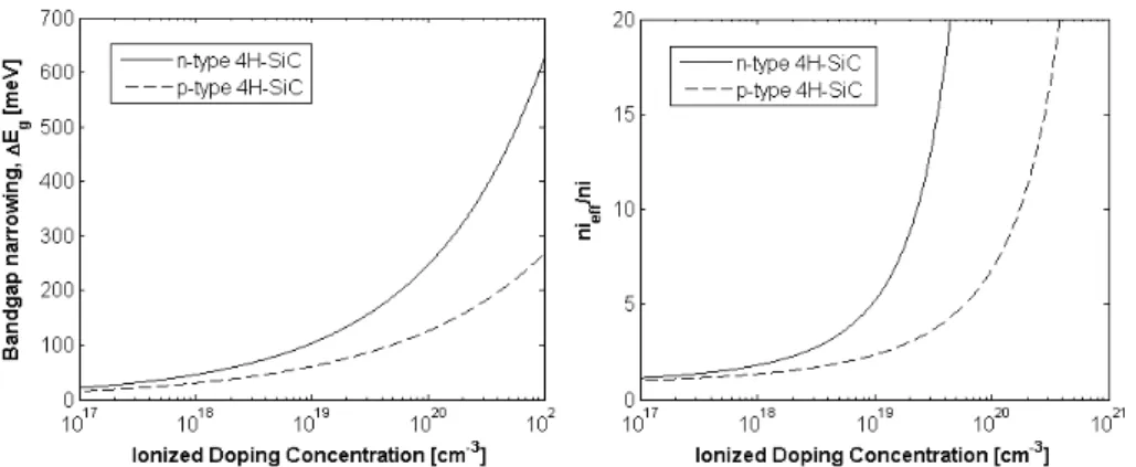
Apparent bandgap narrowing models for calculating the shifts in band edges for 4H-, 6H- and 3C-SiC have been published in the 1998 by Lindefelt [47]. Relatively to 4H-SiC, he quantifies the band edge displacements as a function of the activated doping according to the following expressions: 3 1 18 2 4 1 18 2 18 2 10 10 5 . 1 10 10 9 . 1 10 10 7 . 1 ⎟⎟ ⎠ ⎞ ⎜⎜ ⎝ ⎛ + ⎟⎟ ⎠ ⎞ ⎜⎜ ⎝ ⎛ + = ∆ − D+ − D+ − D+ gd N x N x N x E (2-14a) 3 1 18 2 3 1 18 2 18 2 10 10 57 . 1 10 10 3 . 1 10 10 54 . 1 ⎟⎟ ⎠ ⎞ ⎜⎜ ⎝ ⎛ + ⎟⎟ ⎠ ⎞ ⎜⎜ ⎝ ⎛ + = ∆ − A− − −A − A− ga N x N x N x E (2-14b)
As displayed in Fig. 19, where a direct comparison is done respect to the Si, a larger∆Eg is expected in n-type material for 4H-SiC, whereas
approximately the samedisplacements are obtained in p-type material for both materials. The resultant bandgap narrowing effect and its influence on the intrinsic carrier concentration are shown in Fig. 20.
Fig. 19: Conduction and valence band displacements for 4H–SiC vs ionized doping
concentration in purely n-type (left) and p-type (right) material. For comparison, the band edge displacements for Si are also shown
Fig. 20: Bandgap narrowing in 4H-SiC (left) and corresponding influence on the
2.5 Carrier Recombination Lifetime
In semiconductor materials the generation of electrons and holes in excess is due to thermal activity, electrical and/or light excitation; opposite to this phenomenon, there is the recombination of such carriers, whose rate can be defined by the following expression:
τ
c
U =∆ (2-15) with ∆c the excess carrier density, and τ the recombination lifetime of such carriers. This latter parameter is strongly related to the crystal quality and defects and, since its value quantifies the effect of different processes which conjointly participate to the recombination phenomenon, it is important to use a complete model that includes all the involved recombination mechanisms in order to get an accurate estimation of the effective lifetime.
As shown in the following sections, there are fundamentally three recombination mechanisms which occur in semiconductors, with different intensities: radiative recombination, Auger recombination and recombination through defects in the bandgap [48]. Respect to the latter, the first two are band to band, or direct, recombination processes and they depend only on the concentration of free carriers present in the bulk semiconductor.
The free carrier concentrations (electrons and holes) are defined as:
n=n0+∆n≈ND+∆n for n-typematerial (2-16a) p= p0 +∆p≈NA +∆p for p-typematerial (2-16b) where n0 , p0 are the electron and hole concentrations at equilibrium,
Fig. 21: Radiative recombination process
density of electrons and holes in excess per unit volume. At equilibrium, both excess carrier concentrations must be equal, because the generation process involves the creation of electron-hole pairs, i.e.
p n=∆
∆ . Therefore, at given doping density and illumination level mechanisms, the direct recombination processes are exclusively inherent to the material properties: in this case, the only way to reduce the total recombination rate is through the minimization of the number of defect during the manufacture process.
2.5.1 Radiative Recombination
The radiative recombination consists of the annihilation of an electron-hole pair, which leads to the creation of a photon with energy close to that of the bandgap (see Fig. 21). If the carrier has energy higher than that of the bandgap, the excess energy is released as thermal energy to the lattice. The radiative recombination rate depends directly on the availability of electrons and holes and it is given by:
Urad =β
(
np−ni2)
(2-17) where β is the radiative recombination coefficient.The radiative carrier lifetime results constant at low injection levels, while it is inversely proportional to the excess carrier density at
high injection levels, as can be observed combining Eq. (2-17) with Eq. (2-16), which bring to the followings:
A D low rad N , 1 β τ = (2-18a) n high rad = β∆ τ 1 (2-18b)
Since the Silicon Carbide is an indirect semiconductor, like the Silicon, the radiative process must be assisted by a photon and a phonon in order to simultaneously preserve momentum and energy. This makes the radiative recombination for SiC much less probable respect to the others recombination mechanisms.
2.5.2 Auger Recombination
Auger recombination, that can be considered as the inverse of the impact ionization process, involves three particles (one electron and two holes, or vice versa). It occurs when the energy released by the recombination of an electron-hole pair is transferred to a third free carrier [49], as shown in Fig. 22. In this process, at low injection level, the expression of the recombination rate is related to the excess
carrier concentration and to doping density [50]: n n D2 for n-typematerial
Auger C pN
U = ∆ (2-19a)
2 for p-typematerial
A p p
Auger C nN
U = ∆ (2-19b)
with Cn and Cp the Auger coefficients for electrons and holes.
Therefore, the Auger carrier lifetime at low injection level is given by: 2 , , 1 A D p n low Auger N C = τ (2-20a)
Keeping in count that at high injection levels both carriers participate to the recombination process, the carrier lifetime at these regimes can be expressed as:
1 2 n Ca high Auger = ∆ τ (2-20b)
where Ca =Cn +Cp is the ambipolar Auger recombination coefficient.
Focused on the evaluation of radiative and Auger coefficients, abundant literature exists for the traditional semiconductors, but this is not the same for Silicon Carbide. By our knowledge, estimated and derived values for 4H-SiC can be found just in [51]: they are reported in Table 6, along with values of the traditional semiconductors.
Radiative Recombination Coefficient β [cm3 s-1] Auger Recombination Coefficient Cn,p [cm6 s-1]
Si 2.0E-15 Cn=2.8E-31; Cp=1.0E-31
Ge 5.2E-14 Cn=8.0E-32; Cp=2.8E-31
GaAs 1.7E-10 Cn=1.6E-29; Cp=4.6E-31
4H-SiC 1.5E-12 Cn=5.0E-31; Cp=2.0E-31
Table 6: Radiative and Auger recombination coefficient for different semiconductor
materials [51-52]
2.5.3 Shockley -Read-Hall (SRH) Recombination
The recombination through defects in the bandgap is a process which is the dominant recombination mechanism in semiconductors with indirect forbidden bandgap, such as Silicon and Silicon Carbide.
It results explicitly dependent on the number of imperfections in the crystal, caused by impurities or by crystallographic defects, such as vacancies and dislocations. These imperfections originate intermediate states (see Fig. 23) within the bandgap that act as recombination centers, or traps, for the free carriers. The theory for recombination through these localized traps was for the first time analyzed by Shockley and Read [53] and then by Hall. Their analytical model which describes the recombination rate (SRH-rate) is given by: ) ( ) ( 1 1 2 p p n n n pn U n p i SRH + + + − = τ τ (2-21)
Fig. 23: SRH recombination process with KT E E ie i T e n n − = 1 ; KT E E ie T i e n p − = 1 and
(
)
1 , , − = np th T p n σ v N τ . Here, ETand Ei are, respectively, the recombination center and the intrinsic Fermi energy levels; Nt is the recombination center density; vth is the electron thermal velocity, and σn (σp) is the capture cross section, that is an estimation of how much the electron (hole) must be near to the trap to be captured. Since most of recombination centers are close to the intrinsic Fermi level, Eq. (2.21) can be simplified in:
) ( ) ( 2 i n i p i SRH n p n n n pn U + + + − = τ τ (2-22)
For conventional semiconductors, the SRH carrier lifetimes in the above equations are modelled as functions of doping and temperature by the following [54]: SRH p n p n SRH p n N N , 0 , 0 , 1+ = τ τ (2-23)
where N is the total doping density and the other parameters are fitting values, opportunely chosen for considering the process-dependent factors.
At the present, poor contributes are avoidable in literature focused on the estimations of these values for Silicon Carbide, particularly for
the 4H-SiC polytype. However, although for the intrinsic carrier lifetimes τn0 p, 0 there is not a convergence of opinions, for the SRH
p n
N ,
parameters it is typically used the extracted value for Silicon [55], i.e.
SRH p n
N , =5x1016 cm-3.
2.5.4 Effective Lifetime
With different intensity, depending on the semiconductor topology and technology, all the above recombination mechanisms conjunctly contribute to the final effective carrier lifetime, whose value can be evaluated by the following:
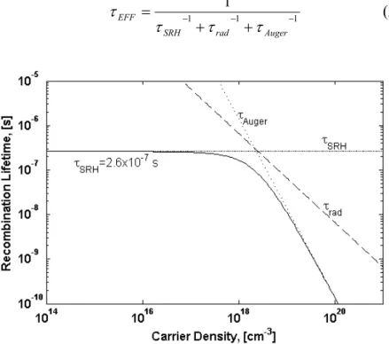
−1 1−1 −1 + + = Auger rad SRH EFF τ τ τ τ (2-24)
Fig. 24: Recombination lifetime in 4H-SiC as a function of the injection level (solid
![Fig. 4: Comparison of Si and SiC power devices for power applications [2]](https://thumb-eu.123doks.com/thumbv2/123dokorg/5729774.74288/19.892.280.788.234.527/fig-comparison-si-sic-power-devices-power-applications.webp)