ALMA MATER STUDIORUM · UNIVERSITÀ DI BOLOGNA
Scuola di Scienze
Corso di Laurea Magistrale in Fisica
Morphological characterization
of ZnS thin films for photovoltaic
applications
Relatore: Presentata da:
Prof.ssa Daniela Cavalcoli Alberto Bartolucci
Correlatore:
Dott.ssa Martina Perani
Anno accademico 2014/2015
Sessione III
I
Contents
Abstract 1
Introduction 3
1 Introduction to photovoltaics 7
1.1 Renewable sources: a global energy solution L . . . 7
1.2 Present status and perspectives of photovoltaicsL. . . 13
1.3 The physics of a solar cell O. . . 14
1.3.1 The solar spectrum O. . . 14
1.3.2 I-V characteristic and main definitions of a solar cellL . . . 16
1.3.3 Homojunction and heterojunctions . . . 20
1.3.4 The Shockley-Queisser limit L. . . 21
1.3.5 Surface passivation . . . . 24
1.4 Solar cells generationsO. . . 27
2 Zinc Sulfide State of the Art 31
2.1 Main characteristics O. . . 31
2.1.1 Crystal structureL . . . 32
2.1.2 Optical properties . . . 32
2.1.3 Dielectric properties . . . 34
2.2 Applications in photovoltaics L. . . 35
3 Materials and Methods 37
3.1 Materials .. . . 37
3.2 Methods . . . 40
3.2.1 Atomic Force Microscopy O. . . 40
3.2.2 Experimental setup . . . 41
3.2.3 AFM modes of operationL. . . 46
3.2.4 Image processing . . . 52
3.2.5 Image analysis . . . 56
3.2.6 Dips analysis L. . . 61
II CONTENTS 3.2.8 EFM – KPFM characterization . . . 66 4 Experimental Results 69 4.1 Morphological characterization L. . . 69 4.1.1 ZnS morphology L. . . 70 4.1.2 ZnO morphologyO. . . 74
4.2 Presence and density of dips . . . 75
4.2.1 Choice of zsegmO. . . 75
4.2.2 Dip analysis resultsL. . . 80
4.3 Structural and grain properties . . . 82
4.3.1 50 W – ZnS_35L. . . 83
4.3.2 75 W – ZnS_36L. . . 86
4.3.3 125 W – ZnS_60 L. . . 89
4.3.4 150 W – ZnS_53 L. . . 92
4.3.5 Choice of segmentation parameters L. . . 95
4.3.6 Sputtering power dependence of the results O. . . 97
4.4 Comparison with ZnO . . . 99
4.4.1 ZnO – Structural and grain analyses results . . . 99
4.4.2 Results comparison and discussion . . . 102
4.5 Electrostatic characterization results . . . . 103
4.5.1 EFM surface topographyO. . . 103
4.5.2 Sheet resistance result L. . . 105
4.5.3 ZnS – Al contact potential differenceL . . . 105
4.6 DiscussionL . . . . 107
Conclusions 109
Acknowledgements 113
1
Abstract
Le celle solari a film sottile rappresentano una delle alternative più promettenti per
un abbattimento dei costi che incentivi significativamente la produzione di impianti fotovoltaici nel prossimo futuro. In questo contesto, la ricerca di nuovi materiali non tossici e più economici per la passivazione delle superfici, necessaria per aumentare l’efficienza delle celle, è di fondamentale importanza.
L’obiettivo di questa tesi è effettuare uno studio approfondito sulle caratteristiche morfologiche ed elettrostatiche di film sottili di ZnS, le cui interessanti proprietà trovano applicazione in svariati ambiti tecnologici, tra i quali dispositivi fotovoltaici ed optoelettronici. Si tratta di un materiale innovativo, le cui proprietà fisiche, nonostante le varie recenti applicazioni, sono state ancora poco studiate.
I film sottili di ZnS analizzati sono stati cresciuti tramite polverizzazione catodica a tensione continua (DC sputtering) a diversa potenza per studiare le connessioni tra condizioni di deposizione e caratteristiche strutturali, le quali determinano le proprietà di questi materiali nel contesto di applicazioni tecnologiche.
Lo studio delle proprietà morfologiche alla nanoscala è stato condotto mediante acquisizione di mappe con microscopia a forza atomica (AFM). Uno dei fattori associati alla qualità dei film è il profilo superficiale, per questa ragione è stata dapprima effettuata un’analisi dei buchi (dips) in funzione della potenza di sputtering, al fine di individuare il campione con la minore densità di dips in vista di applicazioni fotovoltaiche.
I parametri associati alla struttura superficiale, quali la rugosità superficiale, la lunghezza di correlazione laterale e l’esponente di Hurst, sono stati determinati tramite un’analisi statistica delle immagini. I parametri associati ai grani presenti sulla superficie, quali numero e dimensione, sono stati ricavati attraverso un processo di segmentazione delle immagini. Le stesse misure sono state svolte su due campioni di ZnO per comparare i risultati dei due composti.
L’analisi elettrostatica è stata condotta sul campione che ha mostrato la minor rugosità e densità di dips tra quelli analizzati, ed è stata effettuata tramite acquisizione di mappe di potenziale di contatto alla nanoscala con tecnica Electrostatic Force Microscopy (EFM). Un’ulteriore misura con tecnica Kelvin Probe Force Microscopy (KPFM) ha permesso di valutare la differenza di potenziale tra layers di Al depositati sulla superficie del campione e ZnS, corrispondente alla differenza tra la funzione
2 CONTENTS
lavoro di Al e l’affinità elettronica di ZnS. Infine è stata misurata la resistenza elettrica di ZnS con metodo a quattro punte.
Dai risultati morfologici si è ottenuto che la potenza di sputtering influenza significativamente la struttura superficiale, ma senza una proporzionalità lineare. I campioni mostrano una rugosità che varia in modo non lineare tra 0.79 e 3.44 nm e una lunghezza di correlazione in un range da 10.8 a 34 nm. La densità dei grani è risultata variare tra 1100 e 1600 µm-2, con un raggio medio equivalente dei singoli grani che varia tra 12 e 16 nm. I valori ottenuti per i campioni di ZnO mostrano una rugosità molto più elevata e una minor densità di grani.
Per la maggior parte dei campioni analizzati, la lunghezza di correlazione è risultata maggiore rispetto al raggio medio dei grani, da cui si è evinto un processo di clustering degli stessi. Tuttavia si è osservato che ciò non vale per il campione depositato a una potenza di 75 W, il quale inoltre esibisce la minor rugosità e la minor densità di dips. Da ciò si è concluso che potenze di sputtering troppo grandi o troppo piccole in fase di deposizione promuovono il fenomeno di clustering dei grani, di conseguenza aumentandone le dimensioni e incrementando la rugosità superficiale del film. La presenza di grani più grandi risulta correlata ad un maggior numero di dips. Al contrario, superfici composte da grani più piccoli e numerosi risultano avere una minore densità di dips, presentando dunque un profilo superficiale più regolare e con minor rugosità.
Dall’analisi elettrostatica è emersa una corrispondenza diretta tra la morfologia superficiale e il potenziale di contatto, da cui si è dedotto che la densità di carica locale tende ad accumularsi maggiormente in regioni concave. La differenza di potenziale di contatto misurata tra i layers di Al e ZnS è risultata un ordine di grandezza inferiore rispetto ai valori noti da letteratura. Ciò potrebbe essere dovuto alla presenza di stati superficiali indotti dalla formazione di ossidi, sperimentalmente già osservati da studi recenti, che portano a sottostimare la differenza di potenziale reale. Infine, si è ottenuta un limite inferiore per la resistenza elettrica di ZnS di 7 GΩ, andando a confermare le proprietà dielettriche del materiale.
3
Introduction
‘The growing threat of climate change define the contours of this century more dramatically than any other’. This words, said by the US president Barack Obama at the United Nations Framework Conference on Climate Change (UNFCCC) in Paris, in November 2015, define well what many people believe to be among the biggest challenges for human kind in the 21st century. The first challenge is that nowadays the energy consumption strongly depends on fossil fuels like oil, coal and gas. Fossil fuels are not a sustainable energy resource, in the sense that they are not refilled by the nature. More important, by burning fossil fuels the production of greenhouse gases like carbon dioxide (CO2) is promoted 1. According to a major part of the scientific community,
the additional CO2 created by human activities is stored in oceans and atmosphere,
leading to heavy climate changes that if not stopped could cause catastrophic scenarios in the next future. A second challenge is to supply the global energy demand that is rapidly growing with the increase of the world population, which some studies predict to reach 9 billion around 2040 in contrast to the 7 billion people living on the planet today. Especially, the living standard is rapidly increasing in developing countries like China and India, where more than a third of the world’s population is living, according to the data from US Energy Information Administration (EIA) 2.
Finding other sources of energy is of primary importance for both an environmental-friendly consumption and to fill the gap due to the extra energy demand. From this point of view, the development of renewable resources is considered the best alternative to fossil fuels to supply energy in the next future. While all renewable resources will be important, only photovoltaics can provide this level of demand while releasing a low quantity of pollutants. In addition, photovoltaics has been one of the more active field of research in the last decades, with wide opportunities to improve the solar cells performances in order to obtain more energy while lowering material costs 3.
Different semiconductor materials with suitable optoelectronic properties have been found for photovoltaic applications. Silicon is the most commonly used active material for solar cells applications, with over the 85 % of the whole photovoltaic market dominated by crystalline silicon wafer technology. monocrystalline and polycrystalline silicon based solar cells have efficiencies approaching 20 - 25 %. However, despite new technologies that reduce the use of silicon exist, alternative materials and solutions are studied. This has led the photovoltaic industry to produce thin film solar cells consisting of cheaper materials and smaller thickness. The efficiencies reached by the
4 CONTENTS
thin film solar cells result lower than silicon wafer cells, being of about 10 – 15 %. However, the ratio of efficiency to price makes these cells competitive in the photovoltaic market, with wider possibilities to improve the efficiency 3. Thin film solar cells are made by deposition of more thin layers on a rigid substrate, with the presence of passivating material layers in the front and rear surfaces to reduce the surface recombination of minority carriers, which is among the major causes of efficiency loss 4.
Many studies have already proved the crucial importance of the surface passivation, especially for thin film solar cells. Actually, the presence of passivating layers in thin film solar cells technology is essential for a significant efficiency increase, making the implement of an effective passivation method a near-term challenge in the PV industry. Among various suitable materials for surface passivation, Al2O3 has been observed to
increase significantly the efficiency of several types of cells. Recent investigations have led attention on zinc sulfide (ZnS) as a suitable material to be used as passivating layer for thin film solar cells 5,6. The interesting properties of ZnS could be useful in various devices, covering a wide area of applications, among which can be included: antireflection coating for the solar cells, non-toxic buffer layer (compared to CdS layer in CIGS based thin film solar cells), wide energy gap material for electroluminescent and optoelectronic devices, photosynthetic coating and blue emitting laser diodes 7. In this thesis, a morphological characterization of a series of ZnS thin layers at the nano-scale has been performed with Atomic Force Microscopy (AFM) technique to evaluate the main structural features. ZnS thin films deposited on a substrate by DC sputtering at different deposition conditions have been studied in the analysis, in order to measure how those conditions affects the morphological properties of the layers. The surface morphology has been investigated in order to perform a thorough characterization of the surface structure. In the framework of photovoltaic applications, a particular attention has been paid to structural properties related to the surface flatness, i.e. the roughness and density of dips. In addition, the electrical resistance has been measured by using a four-point probes method. Moreover, to get a characterization of the electrostatic profile at the surface, contact potential maps have been obtained by using Electrostatic Force Microscopy (EFM) and Kelvin Probe Force Microscopy (KPFM) techniques.
The contents of the thesis are the following: an overview on the field of photovoltaics, including the current status and future perspectives of technology, the working principles and the main definitions of a solar cell are described in Chapter 1. A description of the material studied, ZnS, with its structural, optical, electric properties, and the actual status of art for technological applications is reported in Chapter 2. The samples description and their properties are illustrated in the first section of Chapter 3. The second section of Chapter 3 is focused on the experimental setup used for all the measurements, the main features of AFM technique, the image processing method and the statistical analysis used to calculate the parameters.
CONTENTS 5
The experimental results of all the measurements on different samples, with a comparison to another Zn compound (ZnO), the morphological AFM images performed and the parameters used during the analysis are reported and discussed. Finally, conclusions about the experimental results have been made.
7
Chapter 1
Introduction to Photovoltaics
In this chapter, an overview on the field of photovoltaics (PV), with its main motivations and applications, has been reported. In Section 1.1, the renewable energies, among which PV represents the most active field of research, are described. The actual status and prospects of PV technology are discussed in Section 1.2. The physics principles behind the solar cells, including the sunlight spectrum, the main circuital characteristics and definitions, the maximum theoretical limit for the efficiency and the surface passivation method, are illustrated in Section 1.3. Finally, a description of the three generations of solar cells with their basic schemes and efficiencies is reported in Section 1.4.
1.1 Renewable sources: a global energy solution
The constant demographic and technological growth that occurred in the last decades has yielded to an enormous increase of the worldwide request of energy. The present global energy consumption per inhabitant has been calculated to be around 6000 kWh per year 8. From the last century, the main sources of energy have been found in exploitation of oil and gas, namely the fossil fuels. With the development of the nuclear energy a new source was found, but the issues associated to radioactive waste have been matter of discussion for a long time, and they are still today. However, for the easiness and the reduced risks associated with their use, human society has relied particularly on fossil fuels during the last decades. It was in 1956 the first presentation of the Hubbert peak theory 9, by which the rate of oil production has been described to follow a curve that reaches a maximum and then declines. Considering that the peak has been proved to have been around the 1970 9, and the amount of oil under the ground in any region is finite, according to the International Energy Agency (IEA) for most
8 1.1 Renewable source: a global energy solution
countries the oil production has already started to decline 10. Moreover, according to the BP’s Energy Outlook 11, the global energy consumption is expected to increase by
34 % between 2014 and 2035.
The massive usage of electrical power generated by fossil fuels has induced climate changes, due to the emission of greenhouse gases into the Earth’s atmosphere. These gases are transparent to incoming solar radiation on Earth, but they absorb and re-emit infrared radiation within the atmospherem causing the global temperature to increase. Greenhouse gases naturally present in the atmosphere consist in water vapor (H2O),
carbon dioxide (CO2), methane (CH4), nitrous oxide (N2O) and ozone (O3), which
except from ozone have largely incremented in recent years according to the European Environment Agency (EEA) 12. Figure 1.1 shows the main climate change due to the
incessant use of fossil fuels. One of the main constituents of the human-emitted greenhouse gases is composed by carbon dioxide (CO2). This is is an important
heat-trapping gas released through human activities such as agriculture and land use changes like deforestation, use of industrial gases and burning of fossil fuels in electricity generation, transport, industry and households 13. Figure 1.1 (a) shows the atmospheric CO2 levels from 2005 to 2016.
Global warming has led to a rise in the average surface temperature by 0.6 to 0.9 °C globally and by about 1 °C in Europe between 1906 and 2005, and the rate of temperature increase has nearly doubled in the last 50 years 14. Without a global action to limit the emissions, the Intergovernmental Panel on Climate Change (IPCC) expects that global temperature may increase further by 1.8 to 4.0 °C by 2100 15. Figure 1.1 (b) shows the global temperature anomaly registered between 1880 and 2015. The 10 warmest years in the 134-year record all have occurred since 2000 13.
The increase in the average temperature has been widely proved to be the main cause of ice melting, with consequent increase of the sea level. Data from NASA’s Grace satellites have shown that the ice sheets in both Antarctica and Greenland are losing mass. The continent of Antarctica has been losing about 134 billion metric tons of ice per year since 2002, while the Greenland loss have been estimated in about 287 billion metric tons per year 13. The Antarctica ice mass variation since 2002 are depicted in Figure 1.1 (c). The melting of ice, jointly with the thermal expansion of the oceans (the increase in volume due to rising ocean water temperature), have inevitably led to the sea level rise. This is an important indicator of climate change, which also increases the probability of storms and endangers coastal ecosystems by flooding flat coastal regions 15. Coastal areas often contain important urban centers and infrastructures. Thus
coastal flooding related to sea level rise could affect a large part of the population 15. Figure 1.1 (d) shows the variation in the sea level from 1993 as observed by satellites.
1. Introduction to Photovoltaics 9
(a)
(b)
(c)
(d)
Figure 1.1: Main climate changes due to global warming: (a) Atmospheric CO2 levels
since 2005 (montly measurements); (b) Global surface temperature change relative to 1951-1980 average temperatures (NASA GISS); (c) Antarctica ice mass variation since 2002 (NASA’s Grace satellites); (d) Sea level change since 1993 (data source: NASA
10 1.1 Renewable sources: a global energy solution
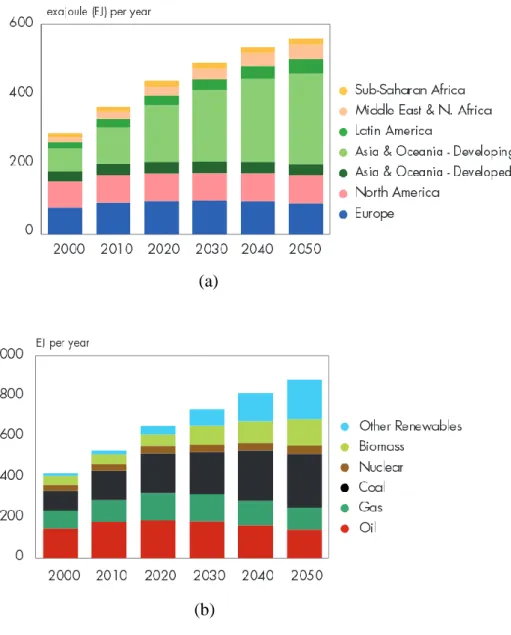
The development of other sources of energy is necessary not only from an ecological point of view, but also by considering the gap between the fossil fuels production and the global energy demand that there will be in the next future. The best possible alternative to fossil fuels today is given by renewable energies, mainly hydroelectric, wind and solar energy, based on the continuing flows from sources of energy that can be approximated as inexhaustible. The world’s largest oil company Shell expects that in the next future a restructuring of the energy industry will take place. In this scenario the global demand of fossil fuels will be still important, but it will reach a plateau by 2020 16. From this moment, renewable energy will become significant. Figure 1.2 shows the energy demand by regions (a) and the energy type of exploitation (b) between 2000 and 2050.
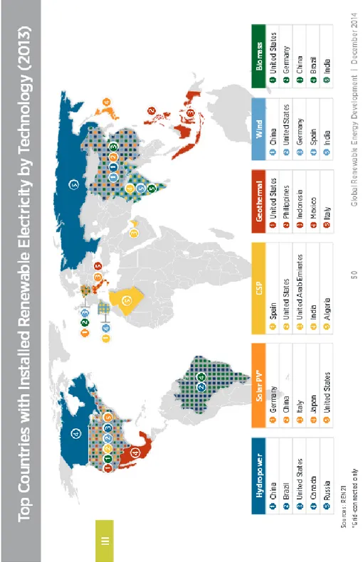
The main advantages of using renewable energy sources over the fossil fuels are a cleaner environment, new employment opportunities, and security of energy supply. Figure 1.3 shows the top countries with installed renewable energy infrastructures in recent years. Emissions of greenhouse gases and other pollutants can be reduced by the use of renewable energy. A collective use of renewable sources of energy would also lead to job creation in the technology manufacturing industries and also in the agricultural sector, which can supply biomass fuel. According to IEA, in 2012 the world relied on renewable sources for around 13.2 % of its total primary energy supply
17. In 2013 renewables accounted for almost 22 % of global electricity generation, and
the IEA Energy Report 2015 foresees that at least 26 % will be reached in 2020 17. Most likely the renewable energy will be one of the worldwide largest sources of energy by 2020, along with gas and nuclear 17. Today, the renewable energy market strongly depends on environment, research and development and market support policies 18. In
Europe the renewable energy industry is a world leading sector, particularly in wind and PV 18.
1. Introduction to Photovoltaics 11
(a)
(b)
Figure 1.2: Energy supply scenarios for the next future: (a) Energy consumption by regions; (b) Primary energy by source 16.
12 1.1 Renewable sources: a global energy solution
Figure 1.3: Top countries with installed renewable electricity by technology in 2013 according to NREL 19
1. Introduction to Photovoltaics 13
1.2 Present status and perspectives of photovoltaics
Among the renewable energies, photovoltaics (PV) is the most promising for the next future. It is non-polluting, requires minimum maintenance and no supervision, and has a long lifetime with low running costs. These and other advantages make PV the best candidate source of renewable energy.
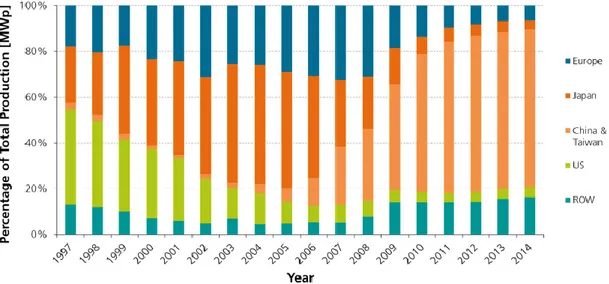
Since 2000, the total production of photovoltaics has increased by almost two orders of magnitude, and the Compound Annual Growth Rate (CAGR) over the last decades has been about 44 % 20. Figure 1.4 shows the annual PV module production by region from 1997 to 2014. Asia is the country with the most rapid growth in annual production over the last five years, where China and Taiwan today account for more than 70 % of the worldwide production20. Figure 1.4 illustrates the evolution of the worldwide
percentage production of PV in the main regions around the world. In the last years, new investments continued to rise in Asia. The leading country in new renewable energy investment was China at USD 54.2 billion (EUR 40.2 billion), followed by the USA at USD 36.7 billion (EUR 27.2 billion) 21.
At the present status, the solar cell technologies are well established and provide a efficiency around 20 - 25 %, with an energy output for at least 25 years. Over 85 % of the actual production employs crystalline silicon wafer technology. In the next future, the entry of new technologies in the market will be the main factor to enable further cost reductions. Hence, to maintain a large growth rate of the PV industry, different solar cell technologies must be developed simultaneously 20. Actually, the majority of thin-film manufacturers remain silicon based and use either amorphous silicon or microcrystalline silicon structure 22.
Figure 1.4: PV module production by region: percentage of total MW peak produced from 1997 to 2014 20.
14 1.3 The physics of a solar cell
1.3 The physics of a solar cell
It was in 1839 when Alexandre Edmond Becquerel discovered the photovoltaic effect, which explains how electricity can be generated using light as a source. After attempts with selenium and cuprous oxide solar cells during the 19th century, a first silicon cell was developed in 194123. However, the first solar cell with a reasonable efficiency of 6 % was announced by Daryl Chapin, Calvin Fuller and Gerald Pearson in 1954 24. During the first decades, solar cells were mainly used as power sources for space applications. It was in the early 1970s that the interest for the solar cells was reconsidered because of the energetic crisis of oil in the western world23.
1.3.1 The solar spectrum
Only photons of appropriate energy can be absorbed and generate the electron-hole pairs in the semiconductor material of which is made a photovoltaic device. The energy of the visible photons of which is composed the sun radiation is sufficient to excite electrons to higher energy levels if the target material has an energy gap lower than the photon energy, but these excited electrons quickly relax to their initial ground state. The collection of the charge carriers generated by the sun radiation is performed by a
p-n junction, which prevents the recombination by using a junction to spatially separate
the electrons from the holes 24. The carriers are separated by an electric field existing at the p-n junction. If the two regions of the cell are connected together, the photo-generated carriers flow through the external circuit to produce a current.
Photons incoming from the sun provide an unlimited energy flow for PV power sources. The solar radiation spectrum, i.e. the number of photons as a function of wavelength, can be described by two parameters, namely the spectral power density
P(λ) and the photon flux density Φ(λ). The spectral power density is defined as the
incident radiation power per unit area and per unit wavelength. The photon flux density is the number of photons per unit area, per unit time and per unit wavelength. These two quantities are related by the following equation 1:
𝛷(𝜆) = 𝑃(𝜆) 𝜆 ℎ𝑐
(1.1)
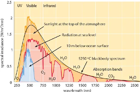
Figure 1.5 shows the spectrum distribution of the solar radiation with various absorption peaks associated to the presence of air molecules in the atmosphere. The temperature at the center of the sun can reach 106 K, while on the surface is about 6000 K. The sun radiation can be approximated to that of a 6000 K black body (i.e. a perfect emitter and absorber of electromagnetic radiation), due to the near total absorption of radiation by the photosphere. The total power density of the solar radiation at the mean earth-sun distance on a surface normal to the sun direction and outside the earth’s atmosphere defines the solar constant or air mass zero (AM0) radiation. Its value is a
1. Introduction to Photovoltaics 15
constant parameter: 1353 kW/m2 1. The earth’s atmosphere attenuates the solar radiation over the 30 %. This is due to absorption and scattering by air molecules, dust particles and aerosols in the atmosphere. Oxygen and CO2 are among the main cause
of absorption, which acts as a wavelength filter. As a result, a different solar spectrum can be measured at the earth’s surface, with the presence of gaps (e.g. ozone filters solar radiation with wavelength below 0.3 µm) 1, as depicted in Figure 1.5. The
importance of this can be understood considering that the wavelength of the incoming solar radiation varies significantly the response of a solar cell. Except from the weather conditions, the main parameter that determines the solar spectrum at the earth’s surface is the distance that the sunlight has to travel through the atmosphere.
The ratio between an actual distance and the minimal path length when the sun is at the zenith is called the air mass. When the path length is the shortest, with the sun at the zenith, it corresponds to air mass one (AM1). At an angle θ respect to the zenith, the air mass can be defined as follows:
𝐴𝑀 = 1
𝑐𝑜𝑠𝜃
(1.2)
The terrestrial solar radiation standard has been defined AM1.5, because of the variability of terrestrial light and to allow comparisons between the performances of solar cells at different locations. The AM1.5 radiation has a power density content of 1000 W/m2, which is close to the maximum irradiance at the earth’s surface. However, the total solar radiation that reaches a particular region on the earth is extremely variable. The diffuse component of the solar radiation, which originates from the scattering with the air molecules in the atmosphere, represents about the 15 % of the total sunlight. The spectrum distribution of the diffuse part consists mainly in the shorter wavelengths. For these reasons, an optimal PV device must be designed depending on the solar radiation availability for each particular location.
Figure 1.5: Spectrum distribution of solar radiation with various absorption peaks due to the presence of the atmosphere (labeled with the associated molecular species) 25.
16 1.3 The physics of a solar cell
1.3.2 I-V characteristic and main definitions of a solar cell
A PV device, or solar cell, involves a contact with different electronic properties that pulls the excited electrons away before they can relax, bringing them to an external circuit. The output potential difference obtained results from the extra energy of the excited electrons, and can be used to do electrical work. The efficiency of the solar cell is directly related to the choice of light absorbing materials and their connections to the external circuit 24. The incoming photons are absorbed by the material to generate charge carriers. The rectifying properties of the solar cell drive the carriers toward the external circuit. An open circuit photo-voltage is made up in this way, and if the terminals are connected a short circuit photocurrent is generated. If a load is connected to the external circuit the cell delivers both current and voltage, which product gives the output power 24.
A solar cell develops a voltage when it is under illumination conditions, for this reason, the surface of a solar cell must result the less reflective as possible in order to absorb the largest amount of radiation. When the terminals are isolated, meaning an infinite load resistance is placed in the circuit, the voltage is called the open circuit
voltage Voc. The current originating when the terminals are connected together without a load is called the short circuit current Isc. Introducing an intermediate load resistance
RL, the cell develops a voltage between 0 and Voc and generates a current I(V) determined by the current-voltage characteristic of the cell under illumination. The photocurrent density results proportional to the illuminated area, as follows by the relation 24:
𝐽𝑠𝑐 = 𝑞 ∫ 𝛷(𝐸)𝑄𝐸(𝐸)𝑑𝐸 (1.3)
where QE(E) is the probability that an incident photon of energy E to send one electron to the external circuit, Φ(E) is the incident photon flux density and q the charge of the electron. The quantity QE is called the quantum efficiency and depends on the absorption coefficient of the solar cell material but not on the incident spectrum, which makes it a key quantity in investigating solar cell performance under different conditions 24. Figure 1.6 shows the QE spectrum of various types of solar cells. A solar cell in the dark under I-V measurements produces an exponential curve that is characteristic of diode, which is called the dark current Idark(V), and possesses an opposite direction respect to the photocurrent. It reduces the net current from the short circuit value. The dark current is also defined as the I-V characteristic of the solar cell under dark conditions, and it results much smaller than the current that it is developed under illumination. This rectifying behavior is the reason for which a solar cell is modeled like a diode. The dark current density for an non-ideal diode results 24:
𝐽𝑑𝑎𝑟𝑘(𝑉) = 𝐽0(𝑒 𝑞𝑉
𝐴𝑘𝐵𝑇− 1) (1.4)
where J0 is the reverse saturation current of the associated diode, A is the ideality factor,
1. Introduction to Photovoltaics 17
Figure 1.6: Quantum efficiency of different technology based solar cells 26.
The expression of the net current can be approximated by the sum of the short circuit photocurrent and the dark current. This step is known as the superposition approximation, which is reasonable for many PV materials. Figure 1.7 shows the I-V characteristic of the solar cell under dark and light conditions. Therefore, the net current density is given by:
𝐽(𝑉) = 𝐽𝑑𝑎𝑟𝑘− 𝐽𝑠𝑐 (1.5)
where the sign of the circuit photocurrent is conventionally taken negative in PV. Substituting the expression for Idark(V) in Eq. (1.5), the net current density results:
𝐽 = 𝐽0(𝑒 𝑞𝑉
𝐴𝑘𝐵𝑇− 1) − 𝐽𝑠𝑐 (1.6)
When the dark current and the short circuit photocurrent exactly cancel out, the potential difference reaches its maximum, which is the open circuit voltage VOC that increases logarithmically with the light intensity, as shown by the following relation 24:
𝑉𝑜𝑐 =𝐴𝑘𝐵𝑇 𝑞 𝑙𝑛 (
𝐽𝑠𝑐 𝐽0 + 1)
(1.7)
When the cell is under illumination, it generates a photocurrent that is proportional to the light intensity. The voltage must lie between 0 and Voc for the cell to generate power, which is the current-voltage product given by:
𝑃 = 𝐽𝑉 (1.8)
The cell’s maximum operating point for P occurs at the voltage Vm, corresponding to a current density Jm, as shown in Figure 1.7
18 1.3 The physics of a solar cell
Figure 1.7: Current-voltage characteristic of the diode associated to a solar cell in dark and light conditions 27.
The ratio of the maximum power from the solar cell and the product of Voc and Jsc is defined as the fill-factor (FF) 24:
𝐹𝐹 = 𝐽𝑚𝑉𝑚 𝐽𝑠𝑐𝑉𝑜𝑐
(1.9)
The FF is a measure of the ‘squareness’ of the solar cell J-V curve. A fundamental quantity for characterize a solar cell is the efficiency η of the cell, defined as the ratio of power output from the solar cell to the incident light power density Pil:
𝜂 = 𝐽𝑚𝑉𝑚 𝑃𝑖𝑙
(1.10)
The efficiency is the most commonly used parameter to compare the performance of different solar cells.
In the equivalent circuit shown in Figure 1.8, the solar cell is modeled as a current generator in parallel with a non-linear resistive element with rectifying properties, i.e. a diode. For a non-ideal cell, the power is dissipated in various ways. The power dissipation of a solar cell can be modeled considering two parasitic resistances, namely the series (Rs) and shunt (Rsh) resistances. Figure 1.8 shows the equivalent circuit for a real solar cell, while Figure 1.9 depicts the effects of the series and shunt resistances on the I-V curve. The main causes of the presence of series resistance involve the contact resistance between the metal and the semiconductor 28. The shunt resistance is typically due to manufacturing defects, meaning the leakage of current through the cell
24. The impact of both the series and shunt resistances in a solar cell is to reduce the FF. In order to have an efficient cell, a small Rs and a large Rsh are required.
1. Introduction to Photovoltaics 19
Figure 1.8: Schematic view of the equivalent circuit for a non-ideal solar cell including series and shunt resistances 29.
Including the parasitic resistance in the Eq. (1.6), the diode equation results 24: 𝐽 = 𝐽0(𝑒𝑞(𝑉+𝐽𝑅𝐴𝑘𝐵𝑇𝑠)− 1) − 𝐽𝑠𝑐+𝑉 + 𝐽𝑅𝑠
𝑅𝑠ℎ
(1.11)
The four quantities Jsc, Voc, FF and η define the main characteristics of a solar cell performance. Measurements made on these parameters must be performed at the same illumination conditions to compare different solar cells. The efficiency depends on the spectrum and intensity of the incident sunlight, and the temperature of the solar cell. Hence, conditions under which efficiency is measured must be carefully controlled in order to compare the performance of one device to another. Terrestrial solar cells are measured under AM1.5 conditions, at a temperature of 25 °C, and with an incident power density of 1000 W/m2. This set of parameters is called the Standard Test Condition (STC). Solar cells intended for space use are measured under AM0 conditions 24.
Figure 1.9: I-V curve of a solar cell with increasing series (Rs) and decreasing shunt (Rsh) resistances. The effect of both resistances is to reduce the FF of the cell 24.
20 1.3 The physics of a solar cell
1.3.3 Homojunctions and heterojunctions
Solar cells use several junction types, all of them with the aim of generating the electric field that acts to separate the charge carriers to extract them in the external circuit. The main devices used for PV applications are the homojunction and the heterojunction 30. Figure 1.10 (a) and (b) show the energy band diagram for a homojunction and a heterojunction, respectively.
A homojunction occurs at the interface between the two parts of a semiconductor material, one n-doped and the other p-doped, are brought in contact to each other. The
n-doped region has a high negative charge concentration, meaning electrons, and the
p-doped region a high positive charge concentration, meaning holes. When the two regions are in contact, electrons diffuse from the n-doped to the p-doped region, while holes flow in the opposite direction. As the carriers diffuse, positive ions in the n-doped side, as well as negative ions in the p-doped side, will form at the junction 30. Hence, a
band bending will occur at the interface between the two doped regions because of the Fermi levels pinning. Then, an electric field is generated at the junction, which sweeps free carriers out. This region is called the depletion region. A built in potential difference due to the electric field is then formed at the junction. This diffusion potential is equal to the difference between the work functions of the two doped regions as follows 30:
𝑉𝑑𝑖𝑓𝑓 = 𝑒𝜙𝑑𝑖𝑓𝑓 = 𝑒(𝜙𝑤𝑝 − 𝜙𝑤𝑛) (1.12)
The work function of a material can be defined as the external energy required to extract an electron from the material, meaning the energy difference between the Fermi level of the material EF and the vacuum level Evac:
𝑒𝜙𝑤 = 𝐸𝑣𝑎𝑐− 𝐸𝐹 (1.13)
If the energy of the incoming photons is larger than the forbidden gap of the semiconductor, namely the energy gap Eg, free minority carrier electrons in the p-doped region and free minority carrier holes in the n-doped region then originate. These minority carriers diffuse toward the junction, where they can recombine with each other or continue to diffuse until they reach the external circuit and generate current. For this reason, a typical homojunction is realized using a thin layer (~0.1µm) for the illuminated part 30. This allows the radiation to penetrate deep in the junction. However, a very thin layer with a high surface to volume ratio could rise some issues because of the large number of surface states that acts as recombination sites for the carriers. A heterojunction is made of two different semiconductor materials, having different energy gaps and electron affinities. For a semiconductor, the electron affinity χ is defined as the energy obtained moving an electron from the vacuum level to the bottom of the conduction band. A fraction of the incoming photons penetrates through the n-doped region toward the p-n-doped region, thus increasing the radiative absorption. This is due to the lower energy gap of the n-doped region respect to the energy gap of the p-doped region 30. However, the use of different semiconductor materials inevitably leads
1. Introduction to Photovoltaics 21
to reticular mismatch at the junction, which increases the probability of recombination for the free-moving charges. Figure 1.10 shows a heterojunction where Eg1 < Eg2 and with the same doping level for the two parts in order to have the same width for the depletion regions. In solar cells using a heterojunction device, the top layer acts as a window layer, that is a material with a high energy gap, which is transparent to the low energy photons. Almost all incident light can penetrate the window layer to reach the bottom layer, which is a material with a low energy gap to absorb another fraction of the photons 30.
(a) (b)
Figure 1.10: Energy band diagram: (a) p-n homojunction (χs is the electron affinity);
(b) p-n heterojunction (χ1 < χ2 and Eg1 < Eg2); The different regions of both the junctions possess the same doping level 30.
1.3.4 The Shockley-Queisser limit
From thermodynamics, the maximum theoretical limit of efficiency for a solar cell is given by a Carnot heat engine operating between the sun temperature (~6000 K) and the cell temperature (~300 K). However, the highest efficiencies reached for solar cells are much lower than the thermodynamic limit, depending on the energy gap, the optical material properties such as the absorbance and geometrical factors.
In 1961, William Shockley and Hans Queisser showed that a lower theoretical limit of efficiency exists for a single p-n junction solar cell, which is known as the Shockley- Queisser (SQ) limit. The SQ limit is derived from the detailed balance principle. In this assumption, the photons absorbed by the solar cell must be compensated by the thermal emission of less energetic photons, since both the hole-electron pair creation and recombination processes are possible 24. The main factors considered by the SQ limit include the black body radiation, the radiative recombination and the energy gap. To improve efficiency, a solar cell must have a high absorption coefficient, which permits
22 1.3 The physics of a solar cell
the cell to be modeled as a black body. Then, at thermal equilibrium a black body radiation is emitted by the cell depending on its temperature. The photons emitted by the cell cannot be re-absorbed, resulting in a loss of the available incoming energy 24. The radiative recombination between holes and electrons is then considered. Even if the radiative recombination is only a fraction among all possible recombination events, then the efficiency of the cell will be reduced with respect to the maximum possible value. The energy gap of the solar cell material is another important parameter that contributes to reduce the efficiency limit 31. Since only photons with an energy higher than the energy gap of the device can generate hole-electron pairs, photons of lower energy do not contribute to the electrical output power of the cell. Moreover, photons with a high energy do not provide their whole energy to the device, since the electrons lose this extra energy by Joule effect, converting it to heat. This provides the main efficiency loss factor for the solar cells. In addition to the radiative recombination considered in the SQ limit, other sources of recombination must be taken into account. Surface recombination plays an important role in reducing the efficiency of thin films solar cells. For this reason, a buffer layer is used in order to passivate the surface and reduce the recombination rate 4. Figure 1.11 shows the maximum theoretical efficiency
with the energy gap of absorber materials reported for comparison.
In the SQ model, the efficiency η is expressed as a function dependent upon four different variables 31:
𝜂 = 𝜂(𝑥𝑔,𝑥𝑐,𝑡𝑠, 𝑓) (1.14)
where ts is the probability that an incident photon with energy higher than Eg will generate a hole-electron pair, the factor f represents all other parameters (i.e. those involving transmission of radiative recombination and the solid angle subtended by the sun), xc is the ratio between the temperature of the cell and that of the sun:
and xg is the ratio of the energy gap Eg to the energy associated to the sun temperature:
Efficiency can then be written as follows:
𝜂(𝑥𝑔,𝑥𝑐,𝑡𝑠, 𝑓) =𝑡𝑠𝑢(𝑥𝑔)𝑣(𝑓,𝑥𝑐,𝑥𝑔)𝑚(𝑣𝑥𝑔/𝑥𝑐) (1.17) where u is the ultimate efficiency (according to an ideal photoelectric process with a
𝑥𝑐 = 𝑇𝑐 𝑇𝑠 (1.15) 𝑥𝑔 = 𝐸𝑔 𝑘𝑇𝑠 (1.16)
1. Introduction to Photovoltaic 23
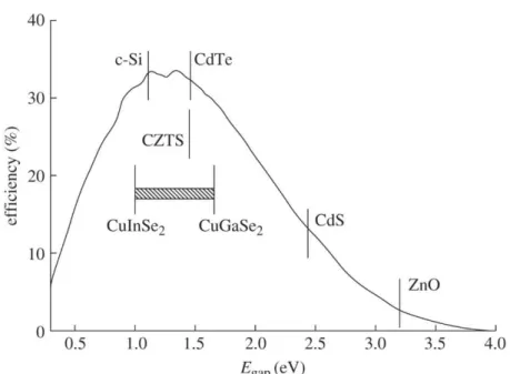
Figure 1.11: Efficiency as a function of the energy gap Eg showing the maximum theoretical value (the SQ limit) for solar cells under AM1.5 illumination conditions without concentration. The energy gaps of absorber materials (c-Si, CdTe, CIGS, CZTS) and window materials (CdS, ZnO) are shown for comparison 32.
single cutoff frequency in a device maintained at 0 K with a 6000 K black-body radiation surrounding it), v is the ratio of the open-circuit voltage to the energy gap of the cell and m is the impedance matching factor, which is a function of the ratio of the ratio of the open-circuit voltage to thermal voltage for the cell 31.
The SQ model proves that a maximum efficiency of 33 % results for solar cells with an energy gap Eg of 1.35 eV under AM1.5 illumination conditions. Suitable absorber materials that have energy gaps in this range include CdTe (1.44 eV) and CuInGaSe2
(CIGS) solutions, which energy gap can be tuned by controlling the In/Ga ratio 32.
Monocrystalline silicon solar cells have already achieved efficiencies close to the SQ limit, while thin films solar cells still have to be improved.
1.3.5 Surface passivation
The surface or interface of a semiconductor possesses discontinuities in the crystalline structure. The partially bonded atoms give rise to many dangling bonds, resulting in a large density of defect levels (or surface states) found within the energy gap at the semiconductor surface. The process of reducing these dangling bonds is
24 1.3 The physics of a solar cell
known as surface passivation. The rate of surface recombination Us, for a single defect can be derived from the Shockley-Read-Hall formalism, given by 33:
𝑈𝑠 = 𝑛𝑠𝑝𝑠− 𝑛𝑖 2 𝑛𝑠+ 𝑛1 𝑆𝑝0 +𝑝𝑠𝑆+ 𝑝𝑛0 1 (1.18)
where ns and ps are the concentrations of electrons and holes at the surface, n1 and p1 statistical factors, Sp0 and Sn0 are related to the density of surface states per unit area
Nts, to the capture cross-sections σn and σp, and to the thermal velocity vth for the specific defect:
𝑆𝑛0= 𝜎𝑛 𝑣𝑡ℎ𝑁𝑡𝑠
𝑆𝑝0 = 𝜎𝑝 𝑣𝑡ℎ𝑁𝑡𝑠 (1.19)
The recombination lifetime τ and the surface recombination velocity S are defined as: 𝜏(∆𝑛) = ∆𝑛
𝑈(∆𝑛) 𝑈𝑠 = 𝑆∆𝑛𝑠
(1.20)
where ∆𝑛 is the excess minority carrier concentration and ∆𝑛𝑠 is the excess minority
carrier concentration at the surface. Neglecting carrier trapping, the excess densities of electrons and holes are equal (∆𝑛𝑠 = ∆𝑝𝑠), which gives 33:
𝑆(∆𝑛𝑠) =𝑛 𝑛0+ 𝑝0+ ∆𝑛𝑠 0+ 𝑛1+ ∆𝑛𝑠 𝑆𝑝0 + 𝑝0+ 𝑝1+ ∆𝑛𝑠 𝑆𝑛0 (1.21)
The quantity S defines the surface recombination velocity that is typically used for quantifying surface recombination processes. A high surface recombination velocity can have a large impact on both the short circuit current and the open circuit voltage since it reduces the minority carrier lifetime. Figure 1.12 (a) and (b) show simulations of the open-circuit voltage Voc as a function of the effective rear surface recombination velocity Seff for solar cells having different cell thickness, in the case of high-efficiency silicon solar cells with a higher minority carrier lifetime τbulk = 750 µs and medium-efficiency silicon solar cells with a lower minority carrier lifetime τbulk = 100 µs, respectively. The result of both trends is an increased importance of an effectively passivated rear surface. It results that the influence of the rear passivation increases when the cells are getting thinner 34.
1. Introduction to Photovoltaics 25
(a) (b)
Figure 1.12: Simulations of the open-circuit voltage Voc as a function of the effective rear surface recombination velocity Seff for a-Si solar cells having different thickness, in the case of high-efficiency cells (τbulk = 750 µs) (a), and medium-efficiency cells (τbulk = 100 µs) (b) 34.
There are typically additional extrinsic surface defects, due to dislocations or chemical residues and metallic depositions on the surface. These defects are sites of several recombination mechanisms, namely surface recombination, Auger recombination and Shockley-Read-Hall (SRH) recombination 33. Thus, passivation of
the cell interfaces improves the efficiency. Figure 1.13 shows the external quantum efficiency spectrum of a Cu(In,Ga)Se2 (CIGS) rear passivated solar cell with different
Al2O3 passivation layer thickness. Actually, the presence of passivation layers in thin
film solar cells technology is essential for efficiency increase, making the implement of an effective passivation method a near-term challenge in the PV industry.
Recombination losses at a semiconductor interface or surface can be reduced by two different passivation strategies. The first is to reduce the number of defects states at the interface by the growth of thin dielectric or semiconductor films. This method is known as the chemical passivation. The second strategy is the significant reduction of the electron or hole concentration at the interface, by means of a built in electric field 33. This electric field can be obtained by either a doping profile below the interface or the
26 1.3 The physics of a solar cell
Figure 1.13: External quantum efficiency (EQE) as a function of the wavelength for a non-passivated and Al2O3 rear surface passivated Cu(In,Ga)Se2 (CIGS) solar cell 35.
presence of fixed electrical charges at the semiconductor interface. As a result, field-effect passivation has limited applications but the field-effect can be employed successfully. In silicon heterojunction solar cells, the passivation is obtained by placing a buffer layer with a larger energy gap between the metal contacts and the active material. In this way the open circuit voltage results increased and higher efficiencies can be reached with lower costs. The passivating layer at the front of the cell is often referred to as the window layer because it should have a high transmittance to let the photons passing through. These buffer layers with a higher energy gap have the role of a semi-permeable membrane for carrier extraction 4. Front surface passivation is typically obtained by chemical vapor deposition of SiO2 and TiO2 layers. However, this requires
very high temperature treatment, which degrades the bulk lifetime significantly as well as the stability of the passivated surface. In addition, SiO2 has a very low refractive
index and it is not a suitable choice for high antireflection coatings. Regarding TiO2, it
does not provide any electronic surface passivation33. Al2O3 has been found as an
alternative material for rear passivation of high-efficiency silicon solar cells 33. Recently, has been demonstrated that an exceptional high-level of c-Si surface passivation can be achieved for SiO2 synthesized at low temperatures when combined
with a very thin Al2O3 capping film. The excellent efficiencies reached (up to 21.3-21.5
%), the high voltages (680 mV), the large quantum efficiency and the high short circuit currents of these cells (40 mA/cm2) have showed the low rate of surface recombination for these devices 33.
1. Introduction to Photovoltaic 27
1.4 Solar cells generations
The first generation solar cells dominated the PV market until the recent years. These devices rely upon high volumes bulk mono-crystalline or poly-crystalline silicon wafers. However, the costs of the materials represent over a half of the total manufacturing costs, with little potential in cost reduction. The basic structure scheme of a c-Si cell is depicted in Figure 1.14.
Silicon solar cells have commercial efficiencies that are limited to around 20 % 36. The efficiency of these cells is approaching the theoretical limit of 29.4 % calculated by recent studies 37. Although efficiency of mono-crystalline silicon (c-Si) solar cells is higher than poly-crystalline silicon (pc-Si) solar cells, production of poly-crystalline silicon wafer is easier and cheaper, making them competitive with mono-crystalline ones 38.
These cells use two different p-type substrates: c-Si and pc-Si. The surface is textured to reduce the efficiency losses associated to incident light reflection. In addition, an anti-reflection (AR) coating of silicon nitride (SiN) or titanium oxide (TiO) is used in order to obtain the maximum reduction of reflectivity. The p-n junction is obtained by a phosphorous doped n-type region on the front surface of the cell and a boron doped p-type substrate. The silver contacts on the front and on the back of the silicon surface collect mobile electrons generated in the silicon bulk and diffusion layers 39.
The second generation of solar cells consists of thin films technology, including amorphous silicon, CdTe and CuInGaSe2 (CIGS). The primary aim of these devices is
to reduce material costs by using cheap semiconductor thin films deposited on low cost substrates to provide acceptable efficiencies of about 10-15 %. CdTe, CIGS and a-Si absorb the solar spectrum much more efficiently than c-Si or pc-Si and use only 1-10 µm of active material 36. The thin-film technology is cheaper but less efficient than the first generation solar cells technology.
28 1.4 Solar cells generations
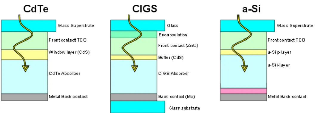
However, the ratio of efficiency to cost results competitive today. In recent years, significant improvements of the thin film technology have been performed, with efficiencies reaching 21 % for CdTe and CIGS devices 20. Figure 1.15 shows the basic scheme of CdTe, CIGS and a-Si thin film PV devices.
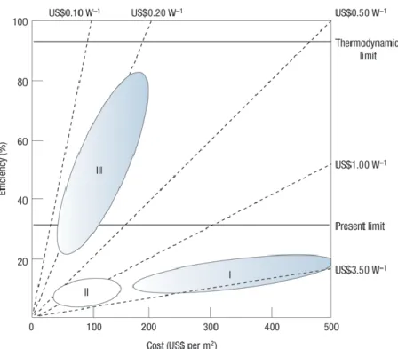
Despite these results, the market of all thin-film technologies has been declining in the last years to about 9 % of the total annual production, while 85 % is held by crystalline silicon 20. In Figure 1.16 the efficiencies reached as a function of the cost for the three generations of solar cells technology are shown.
The structure of both CdTe and CIGS thin film solar cells includes a n-type CdS buffer layer grown by chemical bath deposition on the p-type absorber. The front contact (usually TCO for CdTe and a-Si, ZnO for CIGS cells) serves as a transparent conducting material that collects and delivers the electrons to the external circuit 40. A third generation of solar cells has been developed in the last years exceeding the SQ limit, with reached efficiencies of over 40 %. The main third generation devices include multi-junction (tandem) cells developed in the early 1960s. The tandem cell concept lies in splitting the solar spectrum in ranges of energy in order to use several junctions for the energy conversion. If this technology can be improved reducing the costs, the next future market will be dominated by the third generation solar cells 41.
Figure 1.15: Schematic view of thin film solar cells using CdTe, CIGS and a-Si thin film PV devices 36.
1. Introduction to Photovoltaic 29
Figure 1.16: Efficiency limits of the three generations of photovoltaic cells technology (wafers, thin films and multi-junction) as a function of the areal cost in US$ 42.
31
Chapter 2
Zinc Sulfide State of the Art
Zinc sulfide (ZnS) exhibits interesting properties that have not yet been much investigated. ZnS thin films have been found useful in various devices, covering a wide area of applications, including antireflection coating for the solar cells, non-toxic buffer layer (compared to CdS layer in CIGS based thin film solar cells), wide energy gap material for electroluminescent and opto-electronic devices, photosynthetic coating and blue emitting laser diodes 7. In this section, an overview of the actual state of the art about the ZnS properties and applications, with particular attention for the field of photovoltaics, has been reported.
2.1 Main characteristics
Zinc sulfide (ZnS) is among the first semiconductor materials discovered 43. It results peculiar in various fundamental properties, i.e. a wide energy gap and a high transmittance. It results also a promising alternative material for different applications, including photovoltaic and optoelectronic devices. Its atomic structure and chemical properties are comparable to another Zn compound: ZnO 43. Nevertheless, ZnS exhibits properties that are more advantageous with respect to ZnO. ZnS possesses a larger energy gap (in the range 3.5 - 3.9 eV) than ZnO (~3.4 eV) 43. For this reason, ZnS is more suitable for UV-light based devices such as photosensors, and even more for electroluminescence devices. In addition, ZnS is non-toxic, abundant and cheap. Actually, the properties of ZnS have not yet been investigated in much detail, making this material an actual field of research for further studies.
32 2.1 Main characteristics
2.1.1 Crystal structure
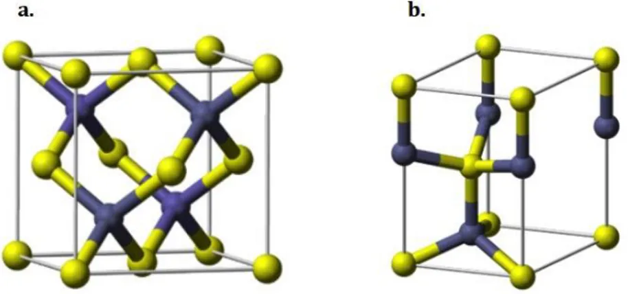
ZnS is found in nature in the mineral of sphalerite. It has commonly two available allotropes: the zinc blende (ZB) cubic form, which is more stable, and the wurtzite (WZ) hexagonal form. The ZB structure results in tetrahedrally coordinated zinc and sulfur atoms stacked in the ABCABC pattern, while the WZ form has the same structure with atoms stacked in the ABABAB pattern 43. Figure 2.1 (a) and (b) shows three different views of the ZB and WZ structures, respectively. The lattice parameters of WZ are a = b = 3.82 Å, c = 6.26 Å and those of ZB are a = b = c = 5.41 Å. The energy gap difference between the two structures is about 0.05 eV 43. The optical spectra, being related to the energy band structure, also results different.
Figure 2.1: Schematic view of the zinc blende (a) and wurtzite (b) crystal structures for the zinc sulfide 44.
2.1.2 Optical properties
Zinc sulfide has a high refractive index of about 2.35 at wavelength of 632 nm 45.
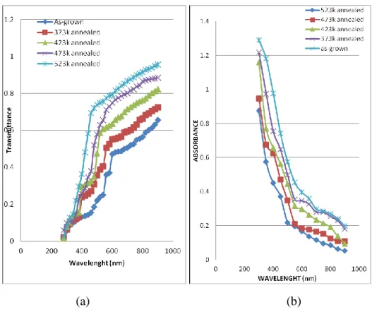
Figure 2.2 (a) and (b) show the transmittance and the absorbance, respectively, of ZnS thin films deposited by Successive Ionic Layer Adsorption and Reaction (SILAR) at different annealing temperatures. The absorbance is low in the visible and near infrared regions, but is high in the UV region, with an enhanced absorption observed close to 360 nm 7. The transmittance is very high in the visible and near infrared regions, and low in the UV region. The high transmittance of about 90 % in the visible range show in Figure 2.2 (a) leads to the conclusion that the ZnS films are actually efficient transmitting and antireflective materials. Figure 2.3 (a) shows the plot of (αhν)2 (where
α is the optical absorption coefficient and hν is the energy of the incident photon) as a
function of the photon energy. Figure 2.3 (b) shows the energy gap as a function of the temperature.
2. Zinc Sulfide State of Art 33
(a) (b)
Figure 2.2: Transmittance (a) and absorbance (b) as a function of the wavelength for ZnS thin films deposited by SILAR at different annealing temperatures 7.
(a) (b)
Figure 2.3: (αhν)2 as a function of the photon energy (a) and energy gap as a function
of temperature (b) for ZnS thin films deposited by SILAR at different annealing temperatures 7.
34 2.1 Main characteristics
The decrease in energy gap with increasing annealing temperature could be attributed to improvement in the crystal quality or to possible variation of the grain size
7. Because of these optical properties, ZnS may play an important role in photovoltaic
devices as buffer layers in CIGS thin film solar cells.
2.1.3 Dielectric properties
Dielectric studies show that the conduction phenomenon in ZnS nanostructures depends on the temperature and the frequency of the external electric field applied 46.
The dielectric constant decreases with an increase in the frequency. In addition, it results much higher than that of the bulk ZnS, which can be treated as an insulator 46. Therefore, the conductivity has the inverse trend. Figure 2.4 shows the dielectric constant and the conductivity plots of ZnS nanostructures as a function of the frequency. All the inhomogenities and defects, together with other phenomena such as space charge formation, produce an absorption current, which results in dielectric losses. The nature of frequency and temperature dependence of AC conductivity suggests an electronic hopping mechanism, which is compatible with the highly disordered or amorphous structure of the grain boundary layers, having high densities of localized levels 47.
Figure 2.4: Variation of dielectric constant (a) and AC conductivity (b) as a function of the logarithm of the frequency for nano ZnS samples at different temperatures 47.
2. Zinc Sulfide State of Art 35
2.2 Applications in photovoltaics
Zinc sulfide (ZnS) has many opportunities for technological applications, e.g. opto-electronic devices such as blue light emitting diodes, electroluminescent devices and photovoltaic cells. Moreover, monocrystalline and polycrystalline ZnS thin films have received particular attention in recent years because of its possible important roles in the photovoltaic technology. One of the advantages of the ZnS films is that they can be easily prepared by several techniques, such as sputtering, molecular beam epitaxy, chemical vapor deposition, thermal evaporation, spray pyrolysis and chemical bath deposition 48.
Today the efficiency of solar cells is one of the most important features in the contest of renewable energy sources. In thin film solar cells, CdS has been the most common semiconductor material used as a buffer layer deposited on top of Cu absorbers. However, the use of Cd is associated to toxic hazards thus leading the attention to new materials having a less impact on the environment to be used as buffer layer. The ZnS is considered one of the most promising candidates among various alternative materials for its non-toxicity, abundance and cheapness 49. In addition, ZnS has a direct wide
energy gap of 3.5 – 3.9 eV at room temperature, which is larger compared to CdS which has an energy gap of 2.45 eV 49.
The efficiency of thin film heterojunctions solar cells strongly depends on the interfacial properties between absorber and buffer layers. The recombination of photo-excited electron-hole pairs that takes places at the surfaces and interfaces is still a limit from this point of view. ZnS thin films can act as excellent surface passivation layers because of their high transmittance, wide energy gap and insulating properties. Due to its low reflectivity, ZnS thin films could also find applications as antireflection coatings, which are essential part of the solar cells. Previous studies showed that the use of a ZnS buffer layer for a CZTSSe monograin solar cell results in similar functionality level as a CdS buffer layer 5. In the experiment reported in reference 5, a higher transmission in the blue light region for the ZnS buffer compared to CdS has been observed. In addition, the substitution of the CdS buffer layer with ZnS, which is a higher energy gap material, has been observed to improve the quantum efficiency of CIGS thin film solar cells at short wavelengths leading to an efficiency of 13.3 % 6. Furthermore, doped ZnS nanoparticles with dimensions below that of the Bohr diameter exhibit interesting opto-electronic properties due to quantum confinement effect and are potential candidates for a variety of applications among which the quantum dot solar cells 45.
37
Chapter 3
Materials and Methods
3.1 Materials
In this work, a sample set of zinc sulfide (ZnS) thin films has been analyzed by Atomic Force Microscopy techinque, which will be described in detail in the following section. In addition, two samples of a different zinc compound, zinc oxide (ZnO) thin films, have been studied in order to compare the properties of the two zinc compounds. ZnS layers are grown by Direct Current sputter deposition (DC Sputtering) using different sputtering power. Zinc sulfides are grown at the Department of Materials Sciences, University of Milano Bicocca, while zinc oxides are grown also by DC sputtering at the Physics Department, University of Konstanz.
Deposition by sputtering is a Physical Vapor Deposition (PVD) technique widely used in the thin film industry. Sputtering method involves the bombardment of a target, made of the material to be deposited, by positive ions which act to remove the material by colliding with its surface 50. Ions are accelerated by gas discharge between two electrodes, where the negative electrode is bombarded by the positive ions generated in the plasma 51. A sketch of a typical sputtering deposition system is shown in Figure 3.1. Sputtered atoms ejected this way can impact the substrate causing the layer to grow. A DC voltage applied in the presence of inert gas (usually Argon) kept at low pressure inside a vacuum chamber provides the discharge that originates the energetic ions 51. The inert gas atoms become positively charged ions attracted to the negatively charged target material at a very high velocity that sputters off particles from the source. These particles cross the vacuum chamber and are deposited as a thin film of material on the surface of the substrate to be coated. Among the main advantages, sputtering deposition technique provides a reproducible deposition control, with the same deposition rate for same value of the parameters involved, meaning an easy film
![Faites vos jeux! Gioco pubblico e società contemporanea: storia, implicazioni, prospettive, a cura di Ornella De Rosa, Editori Laterza, Bari 2018: [recensione]](data:image/gif;base64,R0lGODlhAQABAIAAAP///wAAACH5BAEAAAAALAAAAAABAAEAAAICRAEAOw==)