Università degli Studi di Salerno
Dipartimento di Ingegneria dell’Informazione ed Elettrica e Matematica Applicata
Dottorato di Ricerca in Ingegneria dell’Informazione XIV Ciclo – Nuova Serie
T
ESI DID
OTTORATODegradation of OLEDs
devices: study methods
and solutions
C
ANDIDATO:
E
LENASANTORO
T
UTOR:
P
ROF.
A
LFREDORUBINO
T
UTORENEA:
D
OTT.
M
ARIAG
RAZIAMAGLIONE
T
UTORENEA:
D
OTT.
I
NG.
G
IULIANOSICO
C
OORDINATORE:
P
ROF.
M
AURIZIOLONGO
In loving memory of my cousin Chiara
The greatest enemy of knowledge is not ignorance, it is the illusion of knowledge.
Acknowledgements
I would like to extend my acknowledgements to the many people that in different ways have generously contributed to the work presented in this thesis.
I am sincerely grateful to my supervisor, Prof. Alfredo Rubino, for everything he taught me in these years, always encouraging and helping me to do better. This thesis work would not have been possible without him.
I would like to thank Ph.D. School coordinator, Prof. Maurizio Longo, for his support during Doctoral School in Information Engineering. I remain grateful to Dr. Eng. Carla Minarini, who welcomed me at the ENEA institute in Portici, allowing me to use their working equipment, and supporting me during my permanence at there.
I am profoundly thankful to my ENEA supervisor, Dr. Maria Grazia Maglione who first introduced me to Organic Devices Encapsulation giving me the opportunity to work on this topic and allowing me to learn from all her experience.
I am indebted to Eng. Paolo Tassini for his guidance, for the patience and good advices.
My sincerest thanks go to Dr. Eng. Giuliano Sico, from ENEA, for the long time spent with me, sharing his knowledge, and for being so dedicated to his role as my secondary supervisor. I'm very thankful for his help with permeation topics, for the long hours in the clean room, talking about scientific subjects and lots of other things.
I owe my deepest gratitude to my friend and PhD colleague, Eng. Maria Rosa Fiorillo, for her never-ending friendship, Eng. Salvatore Aprano for his help and all the deposition processes, Dr. Tania Prontera for her friendship, for all the photolithography processes and for the help in experimental moment and Dr. Luca Iannuzzi for the informatics support.
I would like to show my gratitude to all the people met at the institute ENEA Portici who offered me their friendship, helping me and
sharing with me their time and particularly to Martina, Claudia, Maria Laura: it has been a pleasure to meet you all.
I feel thankful towards colleagues and students met during my experience.
And now I want to thank people who have been by my side from the beginning.
My immensurable gratitude goes to people who are always there for me Alessandra, Maria Luisa, Luca and Maria again your friendship has an incommensurable value.
I also would like to thank my volleyball teammates for their constant support when, year after year, I was studying in any possible moment before and after our practices, and even on the road for our matches! The greatest thank goes to my parents, for their unconditioned love and support.
Special thanks to all my wonderful family and to my family in law: we have been one big family from the first beginning.
Finally, I want to thank my husband Sergio. The love he shows me every single moment in good and bad days makes me face difficulties and failures. He always trusted me and my talent even when I didn’t have faith in myself.
There are no words to describe how much I love him.
Thank you all Love you
Table of Contents
Introduction ... 1
1 Organic Electronics ... 6
1.1 Organic semiconductors ... 6
1.1.1 Carbon atom bonds ... 7
1.1.2 Conjugated system ... 9
1.2 Charge Transport ... 10
1.3 Electrical Conduction ... 13
1.3.1 Injection limited conduction ... 14
1.3.2 Space Charge limited conduction ... 16
1.4 Basic Organic Electronics Devices ... 17
1.4.1 Organic Thin Field Transistor ... 17
1.4.2 Organic Solar Cells ... 18
1.4.3 Organic Light Emitting Diode (OLED) ... 20
1.5 Degradation of OLED Devices ... 24
2 Principle of permeation and barrier technology ... 27
2.1. Principle of permeation ... 27
2.1.1 Adsorption and desorption ... 28
2.1.2 Diffusion ... 29
2.1.3 Permeation ... 30
2.2 Permeation Measurement Techniques ... 33
2.2.1 Coulometric Devices ... 34
2.2.2 Mass Spectrometry ... 35
2.2.3 Laser absorption ... 36
2.2.4 Calcium Corrosion Tests ... 36
2.3 Barrier Requirements ... 38
2.4 Encapsulation solutions ... 39
2.4.2 Lamination of film barrier ... 41
2.4.3 Thin Film Encapsulation ... 42
2.4.4 Multilayer approach... 48
3 Development of an Electrical Calcium Corrosion Test measurement system ... 51
3.1 Electrical Calcium test choice... 51
3.2 Layout design ... 52
3.3 Measurement setup ... 55
3.4 Sample realization... 56
3.5 Evaluation of measurement curves and WVTR calculation 58 3.6 Limitation and future perspective of Electrical Calcium Test 60 4 Development of a glass to glass encapsulation system ... 62
4.1 Layout choice ... 62
4.2 Encapsulation process parameters optimization ... 63
4.3 Encapsulation characterization through Electrical Calcium Test 66 4.3.1 Calcium Test results at ambient condition ... 68
4.3.2 Calcium Test results for various conditioning... 70
4.4 Validation of the encapsulation system through device degradation in accelerated atmosphere ... 70
5 Development of a flexible barrier layer encapsulation system .. 75
5.1 Thin Film Encapsulation choice ... 75
5.2 Developing and optimizing of single thin inorganic Al2O3 layer for multilayer barrier structure ... 76
5.3 Developing and optimizing of organic intralayer for multilayer barrier structure ... 80
5.4 Making multilayer inorganic-organic barrier structure on flexible PEN substrate ... 83
Table of Contents iii
6.1 New methodology for intrinsic degradation study ... 87
6.2 Case study: blue OLED devices ... 89
7 Conclusion and future perspective ... 96
7.1 Conclusion ... 96
7.2 Future perspective ... 98
8 Table of Figures ... 100
Introduction
The fast technological evolution of our world requests the necessity to make this development sustainable. In order to achieve this goal more relevance has been given to the energy consumption and environmental impact of the modern society consumerism.
These considerations point out the need to increase the effort in research of unconventional materials, new concept and system architecture for devices that could help to overcome these challenges. Nanotechnologies offer the best chance for this innovation and particularly organic electronics has been encouraged thanks to new attractive properties and promising applications.
Organic materials could be processed in thin film accommodating the issue of preservation of manufacturing energy usage despite from bulky and costly processes of inorganic industries. Fabrication techniques, including spin or spray coating, ink-jet or roll-to-roll printing, can be applied at low-temperature and over large area substrates. This is promising to maximize production throughput and to reduce costs. Also many other advances have been reached in the electronic applications of organic materials such as the spread of
light-weight, transparent, flexible and disposable devices. Particularly, in recent years, OLEDs (Organic Light Emitting Diode) have been successful commercialized both for display applications and light source. OLED-based displays are nowadays commercialized both for high performances cell displays and TVs, becoming the major competitors of other well established technologies, like LCD or LED.
In imaging application, very often Active Matrix approach is used to supply the display. In recent years the use of another Organic Electronics device, Organic TFT (OTFT), has been exploited as Active Matrix driver with encouraging results.
In the last years also OLED-based light source have been introduced on the market. OLED panel technology allows overcoming some of the more critical issues of the preceding technologies such as very low energy conversion, as for incandescence source light, lack of good colors and the use toxic elements as for fluorescent tube and costly manufacturing processes and point light source as for the more recent LED technology.
3 Introduction
Despite all these amazing results, important drawbacks still remain in the field of organic electronic devices. Low charge carrier mobilities or still expensive manufacturing cost, but the more critical is extreme sensitivity to ambient conditions, temperature, light, and particularly oxygen and moisture, which could degrade their optical and electrical characteristics.
This work of thesis sets in this scenario and the aim of this research is the study of degradation phenomena through methodology that leads
to the identification of the different mechanisms of degradation involved, responsible of device short life time.
The present work has been developed focusing the attention on the various degradation mechanisms in OLED and the possibility to use their nature to develop innovative analysis methods. For this purpose has been exploited both extrinsic and intrinsic degradation. Critical issues in this field are the complexity of the involved phenomena and the relatively recent interest of the scientific community in the intrinsic degradation topic.
Through the work organic devices and Calcium test sample have been fabricated and a series of experiments have been carried out to investigate their performance. All devices have been fully processed in the cleanroom (class 100) located at ENEA Portici.
In the organization of the thesis work, after a brief presentation of the main features of organic electronics in Chapter 1, an overview of the basic principles of permeation and typical encapsulation solutions are presented in Chapter 2. In particular, specific attention has been paid on barrier requirements and solutions presented to protect the devices. These solutions, besides being the way to control extrinsic degradation, are also used to isolate other degradation components becoming a tool for studying the intrinsic degradation in organic devices. In the Chapter has been also pointed out the importance to evaluate the barrier characteristic in terms of WVTR and here has been presented some solution to evaluate ultra-high barrier permeation. The study has been then centered on the design and development of a Calcium corrosion test for the barrier evaluation descripted in detail in Chapter 3. It has been investigated all the aspect of layout and setup to achieve a higher sensitivity level. This measurement method has been employed for the design and optimization of both a glass to glass and Thin Film Encapsulation barrier permeation system respectively presented in Chapter 4 and Chapter 5. In the first case (glass to glass) the developed encapsulated system has been used in an effective way to estimate lifetime of a simple OLED structure and validate the system performances.
Afterwards, the investigations have been focused on intrinsic degradation process. For this purpose the glass to glass encapsulation system has been also used to neglect external agents within the development of an innovative method based on accelerated
5 Introduction environmental aging conditions for the study of intrinsic degradation phenomena components. Thus an innovative methodology to study this issue has been proposed and tested on a case study in Chapter 6.
Chapter 1
1 Organic Electronics
In nature we can find a huge variety of materials that have in common they contain carbon known as organic materials. Since some of these organic materials exhibit semiconducting properties they can employed to fabricate electronic devices showing a multiplicity of desirable features made them appealing from both industrial and scientific point of view.
Simple production processes, materials availability and versatility, mechanical flexibility, innovative devices and large area applications combined with cost-effective, reduced power consumption [1] are just a few aspects that made Organic Electronics a research priority of many industries, universities and research institutes worldwide. In this Chapter the basic properties of organic compounds will be described, focusing attention to the semiconducting behavior. Then some organic devices will be shortly presented.
1.1 Organic semiconductors
Almost all carbon-based compounds are classified as organic materials except for few carbon-containing materials such as carbide, diamond, or C60. They can occur in a variety of molecular structures
and, depending on their molecular weight, they are distinguished in small molecules or polymers. Some of those organic materials exhibit semiconducting properties and this motivate their large diffusion. The difference between semiconductors and electrical insulators is due to the size of the energy gap electrons must overcome. In contrast to inorganic semiconductor, organic materials are rarely crystalline and
1.1 - Organic semiconductors 7 the overlap between the orbitals of two molecules is small. Thus the energy levels of the molecules do not split up to whole bands, and the electron mobility, which requires hopping of electrons from one molecule to the next, is low. Due to their low conductivity, organic semiconductors have to be deposited in very thin layers (orders of magnitude ranging from 1 to 500 nm) to keep the driving voltage of the organic devices in the range of some volts. The deposition processes of these thin layers depend on the size of their molecules.
Small molecules are light enough to be thermally evaporated without being decomposed and the desired geometry can be obtained via shadow masks. On the contrary, polymers are larger molecule, hence the van-der-Waals interaction between their single molecules is larger than for small molecules and they decompose below their evaporation temperature. Consequently, those polymers are spin-coated or printed onto surfaces from solutions, and the corresponding solvents are then removed via a curing process. Printing is an excellent process for large-scale applications, but the process is limited to a few layers, since the solvent of further layers should not wash away the layers underneath.
1.1.1 Carbon atom bonds
In organic materials, the semiconducting property originates from carbon atoms bonds. Let us consider the electronic configuration of an isolated atom of Carbon: 2s22p2. When carbon atoms come
together, the s orbitals and tree p-orbitals mix themselves forming equivalent states leading to concept of “hybridization”. If Carbon orbitals form four equal states, tetrahedrally arranged, we are talking about sp3 hybridization [2]. Molecular bonds arising from sp3
and s orbitals (e. g. Methane) are called σ-bonds. They have large binding energies because electrons are strongly localized.
Another possible Carbon configuration is that obtained in the so called sp2 hybridization. In this case only two of 2p states mix with 2s,
obtaining three sp2 orbitals plus a not hybridized p one. They can form
three planar σ bonds while the remaining not hybridized p-orbitals form π bonds. Here electrons are more delocalized (over several atomic units) and binding energies are low, making the π bond weaker than the σ one.
Figure 1.1 - Carbon sp3 hybridization made of three 2p orbitals mixed with 2s
orbital forming four hybridized sp3 states in tetrahedral spatial configuration. Two Carbon sp3 atoms forming σ bond.
Figure 1.2 - Carbon sp2 hybridization made of two 2p orbitals mixed with 2s orbital
forming three hybridized sp3 states plus one un-hybridized 2p orbital. Two Carbon sp3 atoms forming double σ and π bond.
Hence two neighboring sp2 carbon atom share a double bond, a σ bond
and a π-bond. Orbitals' overlap leads to two different electron wave functions: a bonding wave function and an anti-bonding wave function. In the case of σ bond the large orbital overlap leads to a high energy splitting between bonding and anti-bonding states, i.e. a large energy gap. So became clear that the semiconducting property cannot stem from σ bond because of the large energy gap between bonding and antibonding states, but the electronic states of organic molecules are generated from the p orbitals of carbon atoms through sp2
hybridized orbital. The p orbitals are oriented perpendicular to the plane of the sp2 hybrid orbitals. Hence, the p orbitals of two
1.1 - Organic semiconductors 9 only a slight energy splitting between the bonding (π) and anti-bonding (π*) electron wave functions. Consequently, the related electrons are less localized between or outside the atoms than in the strong σ bond. Such an overlap of p orbitals is called conjugation.
1.1.2 Conjugated system
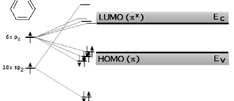
Organic molecules consist of many carbon atoms, (i.e. molecules formed by Carbon rings or chains) that alternating single and double carbon bounds, give rise to the so called conjugated system (or π system) where the π electrons are weakly bound and can be delocalized inside a molecule. Delocalization due to π orbitals is responsible for electrical conductivity. In complex conjugated systems a large number of atomic orbitals overlap, resulting in one group of energy states above and one group of energy states below the energy gap, giving birth to quasi-continuum energy bands made by splitted energy levels.
Figure 1.3 - Band structure of a Carbon ring. It can be seen that an energy gap
occurs from π and π* bonds, while bands formed by σ and σ* states lie at lower and higher energies (respectively).
More precisely the slight overlapping of p orbitals defines the analogous to the valence band and conduction band of an inorganic semiconductor. In detail, the highest π bonding states, that is occupied by electrons and belongs to the lowest group of states, is called HOMO (Highest Occupied Molecular Orbital) and is the lower limit of the gap while the lowest π antibonding state that is unoccupied and belongs to the higher group of energy states is called LUMO (Lowest Unoccupied Molecular Orbital) and represents the upper limit of the
gap. The larger the connected system of π bonds is, the smaller the energy gap becomes. Consequently, modifying the chemical structure changes the energy gap of these molecules; this modification can therefore be used to adjust their emission and absorption behavior. Despite from the behavior described so far, a fundamental and essential difference of conjugated systems from inorganic semiconductor is that the latter have a very crystalline structure made up from single atoms.
Organic materials which exhibit semiconducting properties possess an intermediate structural unit: the molecule. Strong covalent bonds dominate within the molecule, but between molecules, weak van-der-Waals-bonds dominate. The low interaction forces between the molecules have many consequences for the solid but the most important concern the charge transport mechanisms. While in Silicon charges are almost “free” to move over the material, in organic semiconductors electrons and holes have to “hop” from a molecule to another (hopping conduction).
1.2 Charge Transport
The fundamental mechanisms of electron and hole transport in organic solids are not fully understood. Only in the very special case of high material purity, low temperature and high crystallinity, organic materials can exhibit band-like transport behavior similar to that of classic semiconductor. More often organic semiconductors show a disordered structure, so the charge carriers move through an intermolecular process, hopping between adjacent molecules.
Moreover, they can be localized by defects, disorder or potential wells caused by the polarization. If the lattice is irregular or the carrier becomes localized on a defect site, the lattice vibrations are essential to let the carrier move from one site to another. This is an activated process and the mobility increases with increasing temperature. Obviously, the latter is a less efficient mechanism respect to the former.
1.2 – Charge Transport 11
Figure 1.4 - Hopping transport mechanism
Independently from the specific mechanism of electron movement, conduction based on electron movement can be described by the following formulas:
𝐽 = 𝜎 𝐸⃗ (macroscopic description) (1.1) 𝐽 = −𝑞𝑛𝜇𝑒𝐸⃗ (microscopic description), (1.2)
where J is the current density, σ is the conductivity, q is the elementary charge, ne electron density, µe electron mobility defined
as:
𝜇
𝑒=
𝑣𝑑𝐸⃗ (1.3)
and vd is the drift velocity of electrons.
In the first expressions, the macroscopic conductivity refers to a density of electrons that move, on the micro-scale, with the drift velocity. The mechanism of electron movement is hidden within the electron mobility µe that represents the relation (ratio) between applied
field strength and drift velocity.
Focusing on the most common case of disordered organic materials, it is here illustrated two models applied to describe the hopping conduction mechanism: the Nearest Neighbor Hopping (NNH) and the Variable Range Hopping (VRH). In the former, an electrical charge
“jumps” from a spatial localized energy level to the nearest neighbor (Figure 1.5. a), while in the latter the charge can jump several levels away from the original one, i.e. variable range (Figure 1.5. b)
Figure 1.5 - Hopping conduction: a) nearest neighbor hopping, b) variable range hopping.
The transition probability from one energy level to another is expressed as the product of some terms, taking into account:
wavefunctions overlapping between states: this term has an exp(-αR) dependence, where α-1 is the wave function localization length and R is the distance between initial and final levels;
Phonons availability: if the initial and final states have energy separation of W, energy conservation rules require a second particle bridging this gap, in order to enable the charge hop. This mechanism is generally fulfilled through molecules vibration, i.e. phonons. The term dependence is exp(-W/kBT),
where kB is Boltzmann constant and T is temperature;
The probability per unit time of a charge jumping between two localized states is therefore proportional to:
𝑝~ 𝑒𝑥𝑝(−𝑄) (1.4) 𝑄 = (𝛼𝑅 + 𝑊
𝑘𝐵𝑇) (1.5)
When W is smaller than kBT, the αR term dominates, leading to a
NNH mechanism; Q is minimized for minimum R, when the final level is the nearest one. On the other hand, when T is low and phonons
1.3 – Electrical Conduction 13 energy and number are small; W/kBT cannot be neglected with respect
to αR. In this situation, balancing energy and distance, a distant level could possess a smaller Q than the nearest neighbor and a VRH regime occur.
Hypothesizing a casual diffusive mechanism as driving force of electron motion electrical conductivity (σ) in hopping regime can be calculated as follow: 𝜎 = 𝑞𝑛𝜇 (1.6) 𝜇 = 𝑞𝐷 𝑘𝐵𝑇 (1.7) 𝐷 =1 6𝑝𝑅 2 (1.8)
Here, q is electron charge, n is electron density and μ is charge mobility, determined by Einstein relation. D is diffusion coefficient, in which hopping probability is taken into account according to NNH mechanism. On the contrary, in the case of VRH regime, conductivity has the characteristic temperature dependence expression
𝜎 = 𝜎0𝑒𝑥𝑝 [(− 𝑇0 𝑇) 1 4 ] (1.9)
where T0 and σ0 are constant given by model parameters (R, α, etc.).
1.3 Electrical Conduction
In order to understand the electrical behavior of organic devices, electrical conduction could be represented using a huge variety of current-voltage models.
These models essentially belong to two families of phenomena that limit the conduction: injection limited conduction and bulk limited conduction.
1.3.1 Injection limited conduction
When current is determined by injection properties over a potential barrier, we can use the following models [3]:
Thermionic emission Charge carriers are driven by diffusion over a potential barrier. Here, A* is Richardson effective constant, T is temperature, k is Boltzmann constant, Φe is potential barrier height, n
is ideality factor, J is current density and V is applied voltage 𝐽𝑇𝐸 = 𝐴∗𝑇2𝑒𝑥𝑝 (−Ф𝑒
𝑘𝑇) [( 𝑞𝑉
𝑛𝑘𝑇) − 1] (1.10)
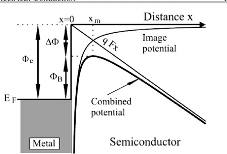
Schottky-Richardson thermionic emission The basic thermionic model is modified for field-assisted emission over the potential barrier. Here, A* is Richardson effective constant, T is temperature, k in Boltzmann constant, Ф𝑒 is barrier height, d is device thickness, q is electron
charge, ε is electrical permittivity of material, J is current density and V is applied voltage. A uniform electric field (E) distribution is considered, i.e. 𝐸 = V/d 𝐽𝑆𝑅 = 𝐴∗𝑇2𝑒𝑥𝑝 (−𝜙𝐵 𝑘𝑇) (1.11) 𝜙𝐵 = 𝜙𝑒− √4𝜋𝜀𝑥𝑞V 𝑚 (1.12) ∆𝜙 = √4𝜋𝜀𝑥𝑞V 𝑚 (1.13)
1.3 – Electrical Conduction 15
Figure 1.6 - Schematic of barrier level for Schottky-Richardson thermionic
emission
Fowler-Nordheim tunneling This is a field-assisted tunneling over a triangular potential barrier. Here, CFN is the Fowler-Nordheim constant, ħ is reduced Planck constant, φe is potential barrier height, d is device thickness, q is electron charge, m* is electron effective mass, J is current density and V is applied voltage. A uniform electric field (E) distribution is considered, i.e. E=V/d
𝐽𝐹𝑁 = 𝐶𝐹𝑁( 𝑉 𝑑) 2 𝑒𝑥𝑝 (−4𝑑√2𝑚∗(𝑞𝛷𝑒) 3 2 ⁄ 3𝑞ħ𝑉 ) (1.14)
Figure 1.7 - Schematic of barrier level for Fowler-Nordheim tunneling
1.3.2 Space Charge limited conduction
When current is determined from material bulk conduction properties, we can take into account the following models:
Nearest Neighbor Hopping conduction (NNH) Here J0 is a constant
depending on material properties, R is NNH distance, d is device thickness, VT is thermal voltage, J is current density and V is applied
voltage. A uniform electric field (E) distribution is considered, i.e. E=V/d.
𝐽𝑁𝑁𝐻 = 𝐽0𝑠𝑖𝑛ℎ ( 𝑅𝑉
𝑑𝑉𝑇) (1.15)
Space Charge Limited Conduction (SCLC) This originates when in a material is injected more charge than that thermally generated. Here, μ is mobility (considered constant with electric field), d is device thickness, ε is electrical permittivity of material, J is current density and V is applied voltage
1.4 – Basics Organics Electronics Devices 17 𝐽 =9
8𝜀𝜇 𝑉2
𝑑3 (1.16)
This expression is valid in the case of a Trap Free material and the model is known as TF-SCLC. Typically an organic material is not trap free but they are present and limit the current. The carriers are captured occasionally by shallow traps and are remitted back thermally: this effect is significant as the level of trap is close to the conduction band. On the other hand the deep traps, however, are located below the Fermi level and for this reason they tend to be occupied and to localize the charges. When all the traps are filled, the current is no more under traps influence, and has a trend formally identical to that in absence of trap states. Modifying the expression to include the effect of the traps in SCLC model it is sufficient to replace the mobility μ with an effective mobility μeff.
1.4 Basic Organic Electronics Devices
In spite of organic materials low conductivities and lower transport performances, through the past years, almost all typology of inorganic devices have been realized employing organic semiconductor obtaining very interesting results.
1.4.1 Organic Thin Field Transistor
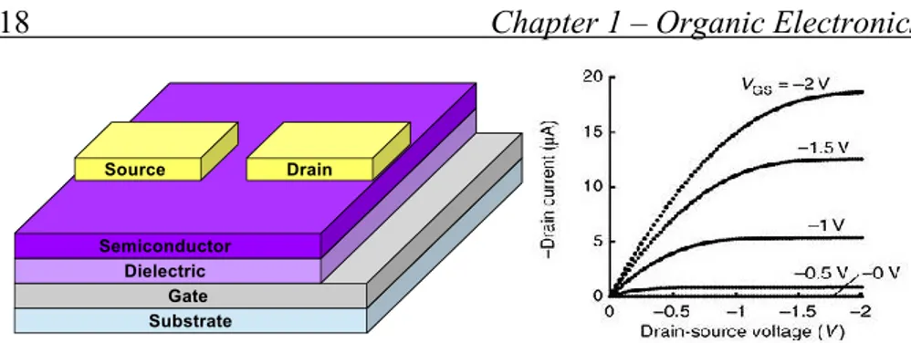
Organic Thin Field Transistors (OTFT) electrical behavior is conspicuously similar to classics FETs. They are three terminal devices where current between two electrodes, i.e. source and drain, connected with the semiconductor, is controlled by modulation of channel conductivity, performed by another voltage applied to an insulated gate electrode.
Figure 1.8 - OTFT in top contact configuration and typical OTFT curves
OTFTs are “normally-on” devices; i.e. without any voltage applied to the gate there is still a current flow between source and drain. Appling a gate voltage of proper bias charges move away from the channel, forming a depletion region that stops the source drain current. Different configurations of OTFTs exist, depending on the deposition sequence of the different layer and the position of electrode.
Figure 1.9 - Four possible configurations for an OTFT.
OTFTs have been successfully used as drivers in AM displays and their field of application is continuously and rapidly enlarging.
1.4.2 Organic Solar Cells
Organic devices expanded in the field of renewable energy, with Organic Photovoltaic (OPV). Also in this case, device basic principles
Substrate Gate Dielectric Semiconductor
1.4 – Basics Organics Electronics Devices 19 are essentially similar to their inorganic counterparts: light enters a semiconducting material and photons with energies above the energy gap are absorbed and thereby generate electron-hole pairs (excitons). These excitons have to split up to generate a free electron and a free hole. Thus, if the organic material is to serve as an electron donor in OPVs, a second material is required as an electron acceptor to ensure a built-in internal field at the interface to break up any excitons that diffuse there into free carriers, both of which are conducted to opposite electrodes. This D-A interface concept is analogous, in terms of charge transport, to a P-N junction in an inorganic semiconductor [4].
The electrical potential difference between electrons and holes at these electrodes is used as an electrical power source when the electrodes are connected over an external circuit. Of course only photons with energies larger than the energy gap excite electrons. On the other hand, photons with energies below the energy gap cannot create excitons. For those photons, the semiconductor is transparent.
Hence, single solar (i.e. single junction) cells cannot convert all of the light energy to electrical energy [5]. The problem can be reduced by using tandem cells, wherein a cell with a large energy gap at the front efficiently extracts the energy from high-energy photons, and a cell with a small energy gap behind the first cell efficiently extracts the energy from the transmitted low-energy photons.
Figure 1.10 - Schematic of device structures of conventional multi-junction tandem
At present, most used single cell configurations are conventional and inverted device structures based on indium tin oxide (ITO) electrode .
Figure 1.11 - Schematic of device structures of (a) conventional single-junction cell,
(b) inverted single-junction cell [4]
OPV efficiencies have recently reached up to 12% and following efficiency growth trends, organic cells improvements have been wider than the amorphous Silicon, so that OPV could replace that technology in coming years.
1.4.3 Organic Light Emitting Diode (OLED)
Organic Light-Emitting Diodes (OLEDs) represent perhaps the most promising application of organic electronic. OLEDs become more and
1.4 – Basics Organics Electronics Devices 21 more popular thanks to their application into high performances displays, but are now used in lighting application due to some obvious benefits. First OLEDs emit light from an area, more pleasant to the eye than point sources of light, and then their color is easily tunable within a wide range via the choice of emitting materials. Even as white light sources they were shown to reach efficiencies comparable or better than fluorescent tubes. The principle beside these devices is very simple: charges (electrons and holes) are injected from the electrical contacts into the organic layers, where they interact and recombine emitting photons. This phenomenon is called electroluminescence (EL), to distinguish it from other kinds of luminescence being produced by different sort of excitations (optical, thermal, chemical, etc.).
Figure 1.12 - Schematic of a bottom up OLED structures
In OLEDs structure at least one of the electrodes must be transparent in order to make the light visible from outside. Depending on the position of transparent electrode, we can have two different device configurations. The most common device structure is called bottom-emitting architecture, using the transparent electrode between the device and the transparent substrate (typically glass, but also plastic materials as PEN or PET have been exploited), making the other electrode of highly reflective metals deposited over the organic
Substrate Anode Hole Injection Layer Hole Transport Layer
Source Drain
Emitting Layer Electron Transport Layer
Electron Injection Layer Cathode
layers on the top of the structure. The other architecture, known as top emitting, can be obtained reversing electrodes properties; i.e. the top contact must be transparent. This solution is less used because of the technological issues connected to the realization and patterning of a transparent conductive layer (very thin metal layers or Transparent Conductive Oxide TCO) without damaging the previously deposited organic layers.
OLEDs can also be classified depending on the molecular weight of the employed organic semiconductor. Small molecules OLEDs (SMOLED) have been exploited first [6]. The most used technique to deposit Small molecules OLEDs is thermal evaporation in high vacuum. Typically complex multilayer systems are used to reach high device efficiency, where various functions like charge transport, recombination, etc. are performed by different materials.
A schematic description of small molecules multilayer OLED with the function of each layer has been reported in figure 1.11. Obviously not always all the depicted layers are present, because the different functions may be combined in one material [7].
Figure 1.13 - General multi-layer sequence for small molecules OLEDs.
The Emission Layer (EML) is generally located in the middle of the device and has the function to let carriers interact among each other (recombine) in order to emit light. The recombination process involves the formation of an excited molecular state known as exciton. The more excitons are allowed to decay radiatively, the more the device efficiency will be improved.
Before reaching the EML, holes are injected from a high work function anode into the HOMO level of an organic semiconductor having a comparably high hole mobility (the Hole Transport Layer, HTL). On the other side of the device, electrons are injected from a
1.4 – Basics Organics Electronics Devices 23 low work function cathode into an organic material with high electron mobility (the Electron Transport Layer ETL). Usually ITO (transparent and conductive oxide) is used with good results as anode electrode and it is a common choice in bottom-emission layout. On the cathode side the more suited metals, but prone to degradation, are calcium, magnesium or cesium. Often these materials are used combined with more stable aluminum or silver.
In order to improve the injection, a thin Hole Injection Layer (HIL), can lower the energy barrier between anode and HTL HOMO level. Electron Injection Layer (EIL) performs the same purpose for electrons. To further improve injection and transport, electrical doping of HTL and/or ETL can be applied as well. Before getting to the EML, holes can pass through another layer, the Electron Blocking Layer (EBL). In the same way, electrons have to pass through a Hole Blocking Layer (HBL). EBL and HBL are not always present in the device structure but at the same time they are often important to reach high device efficiencies. Three fundamental functions are performed by blocking layers:
prevent leakage of the opposite charge carrier type from the EML into the transport layers, forming heterojunction energy barriers in the LUMO-HOMO levels;
spatially separate the excitons in the EML from doped HTL-ETL (because dopants often act as effective luminescence quenchers, forcing a non-radiatively decay of excitons); realize exciton confinement in the EML.
Polymer OLEDs, differently from small molecules devices, are typically processed through spinning or different coating deposition techniques, where the solvent is removed by annealing steps.
Polymer devices are limited in their complexity because of the used solvents that are frequently harmful for the underlying layers. Simple structures employing only a single active layer, where various materials having different functionalities are blended, sandwiched between the electrodes are often used.
In order to improve the general complexity of wet-processed devices, tremendous efforts are spent on improving polymer processing. These efforts include the use of cross-linking polymers to enable deposition of sequential layers from solution, cross-linking in
connection with direct photolithography to achieve patterned polymer layers, and the laser-induced forward transfer of individual device pixels. Besides these uniform coating techniques, printing techniques, derived from publishing, can be used to process polymer-based devices. A compromise is often found in the combination of solution processes and thermal evaporation to achieve multilayer OLEDs that partially consist of layers that comprise solely low molecular weight materials. Finally, similar to small molecules OLEDs, the preparation of the highly reflective cathode requires thermal evaporation in high vacuum [7].
1.5 Degradation of OLED Devices
Despite all the advantages shown by Organic Electronics the most critical issue is devices short lifetime that makes them not suitable for large commercialization. This is especially true for OLEDs. Typically, OLEDs degradation can be induced by two different and independent mechanisms: extrinsic or intrinsic degradation [8] [9]. Extrinsic degradation is strictly connected to the rapid degradation of both organic layers and low-work function metals that suffer when they are exposed to atmospheric oxygen and water vapor. Such deterioration leads to the generation of non-emissive regions, also known as dark spots (Figure 1.14), that lead to a decrease in luminance as a result of losses in the emissive area of the device [10] [11].
Figure 1.14 - Dark spot formation
The main cause of such degradation is connected to the cathode. Either the low work function cathode corrodes and obstructs further
1.5 – Degradation of OLED devices 25 injection or it delaminates from the organic stack. As has been observed, water is more critical than oxygen for OLEDs because water reacts and the releasing hydrogen gas that accumulating beneath the cathode, forces the metal to delaminate leading to the “bubbling” or “domelike” structure often observed in OLED cathode [8] [12].
In order to control extrinsic degradation, a proper protection of the devices is essential. The protection is realized isolating the devices from the environment using barrier materials; such method is known as encapsulation. This technique remains still a challenge, especially in the case of devices deposited on flexible substrates. In fact, materials used for the encapsulation system must assure transparency, flexibility and extremely low values of gas transmission rate, particularly water vapor (WVTR, Water Vapor Transmission Rate), such to ensure acceptable lifetime of the devices for commercial use.
As pointed out before, higher sensibility of OLEDs against water vapor than oxygen has been observed, so WVTR is mostly used as a barrier criterion [13]. Proper design of the encapsulation system is strictly required taking into account the relative sensitivity of the specific device to the atmospheric environment (OLED, OPV, OTFT), the type of substrate support (flexible or rigid) and the operating conditions.
The other degradation mode, intrinsic degradation, refers to the progressive decrease of the luminance over time without any other evidence of degradation in the device appearance. The understanding of the origins of the intrinsic degradation still remains a challenge and up to now, only few mechanisms have been proposed to describe intrinsic degradation. Unlike the previous mechanism, which is essentially attributed to external factors, and involve processes that are independent from the specific organic material system, intrinsic degradation is primarily material dependent. Thus, although some of the few mechanisms that have been identified for a particular material system are expected to extend to other systems, experimentation has yet to prove that [8].
Until now the proposed mechanisms to explain intrinsic degradation involve some unrelated factors that include: (i) morphological and thermal instability (any changes in the bulk properties of emissive layer can affect the radiative recombination), (ii) trap formation (interfacial trapped charges affect the electric field distribution and hence the injection properties), (iii) anode instability
(any changes in the injection contact will affect the carrier injection efficiency and hence the carrier profile) [9]. In these mechanisms, the decrease in the electroluminescence has been observed during device operation.
Nowadays this represents the most open issue in the field of OLED degradation research, depending both on the complexity of the phenomena and on the relative novelty of the topic.
In the following sections extrinsic degradation mechanism and relative solution will be presented first. The comprehension of this phenomenon is unavoidable to face the study of mechanism behind more complex intrinsic degradation.
Chapter 2
2 Principle of permeation and barrier
technology
In order to understand the degradation mechanism and to study the permeation through polymeric materials (organic) and hybrid systems (organic-inorganic), it is essential to describe the basic physical background of permeation. In this chapter has been described first the basic principle of permeation. Then measurement techniques for ultra-low values of WVTR are presented. Finally the most used solution, for barrier encapsulation technologies, together with some of the most used barrier deposition technique are displayed in the subsequent sections.
2.1. Principle of permeation
Permeation is the mass transport of a gas or liquid, the permeate, through a solid. Permeation is a very complex process consisting of three separated phases [14] known as:
• adsorption: from the high concentration area the permeate is adsorbed at the surface in contact with the solid and dissolved into it.
• diffusion: The permeate diffuses through the solid in a random-walk through diffusive jump.
• desorption: The permeate is desorbed from the surface of the solid from the low concentration area.
Assuming constant the concentration gradient, the diffusion process then requires some time to reach a steady state, time needed for the saturation of available space within the polymer for the diffusion.
Figure 2.1 - Schematic of the permeation process
2.1.1 Adsorption and desorption
Adsorption phase is the process of gas bonding on the surface. Either weak or strong bond are possible on the surface. On the other side desorption is the release of the gas from the surface. Since the gas molecules are bonded to the surface, an activation energy is needed for desorption. At room temperature only gases bonded by weak bond can be desorbed.
The equilibrium concentration of the sorbed penetrant c, can be related to the ambient pressure p by:
2.1 – Principle of permeation 29 where the solubility coefficient 𝑆(𝑐, 𝑝) is a function of p and could be described by several sorption models [15]. For an ideal system and low concentration of sorbed penetrant, S can be described by Henry’s law and is independent from p and c. In this case, the relation between c and p (isotherm plot) results linear. For non-ideal systems the absorption isotherm is generally non-linear. Some possible non-linear isotherms are showed in Figure. 2.2.
Figure 2.2 - Typical isotherm plots of sorbed concentration versous ambient vapour
pressure: (I) Henry’s law; (II) Langmuir equation; (III) Flory-Huggins equation; (IV) BET equation [16].
2.1.2 Diffusion
Diffusion is the directed mass transport of randomly moving particles [17]. It is induced by a gradient of concentration. Diffusion can occur via defects, like micro-cracks, or through the bulk material itself. Diffusion through the bulk is negligible for inorganic materials, because their bulk diffusion coefficients are orders of magnitude
lower than their effective diffusion coefficients as a result of defects in the material structure. On the contrary, diffusion through the bulk material is an important issue for polymers. The particles can be seen as jumping from one site to another passing over a potential barrier separating one position from the next. These positions can result from a rearrangement of the polymer chains. This is possible for polymers at room temperature because the polymer chains stick together via weak van-der-Waals-bonds and the activation energy needed for a rearrangement is therefore low. The diffusion through polymers is much more important than the sorption, and consequently limits the permeation [18]. Thus, permeate concentrations at the surfaces are defined only by the sorption and can be treated as constant for diffusion calculations.
Diffusion through a homogeneous diffusion medium, meaning polymers but not inorganic barrier layers, is described by Fick’s laws. Fick’s first law of diffusion describes the flux in z-direction depending on a concentration gradient at any point or plane in the diffusion medium [17]:
𝐽 = −𝐷𝑧 ( 𝜕𝑐
𝜕𝑧) (2.2)
where J is flux of the permeate, D (cm2 s-1) is the diffusion coefficient also indicated as Fick’s coefficient.
2.1.3 Permeation
Combining Fick’s first law with the continuity equation Fick’s second law of diffusion is obtained. It describes the evolution of the permeant concentration over time [17]:
𝜕𝑐
𝜕𝑡 = −𝐷𝑧 ( 𝜕2𝑐
𝜕𝑧2) (2.3)
These equations are fundamental for unidirectional diffusion in an isotropic continuum when the diffusion coefficient D is constant and independent from z, t or c. Actually in many penetrant-polymer systems D is not a constant but is a function of c, the spatial
2.1 – Principle of permeation 31 coordinates and t. Anyway most commonly D is only dependent on the sorbed penetrant concentration.
When Henry’s law is obeyed, using it in the equation for the flux it has been derived:
𝐽 = 𝐷𝑆∆𝑝
𝑧 (2.4)
where ∆𝑝 is the difference between partial pressure over the substrate and z is thickness of the film. The product 𝐷𝑆 defines the permeability coefficient P, so that the relation above becomes:
𝐽 = 𝑃∆𝑝
𝑧 (2.5)
Since the diffusive flux J can be also defined as the total amount passing through a plane surface of unit area normal to the flow direction during unit time and written as:
𝐽 = 𝑄
𝐴𝑡 (2.6)
where Q is the total amount of penetrant which has passed through area A during time t. The permeability P can be then written as:
𝑃 = 𝑧
𝐴∆𝑝 ∆𝑄
∆𝑡 (2.7)
such that the permeability constant can be calculated from linear part of the Q versus t curve.
Furthermore when a penetrant diffuses through a polymer film in which it is soluble, there is a transient state from the time the penetrant first enters the film until the steady state is established. T intercept on the time axis of the extrapolated linear steady state portion of the curve is called lag time, L.
Figure 2.3 - Typical permeation curve: amount of permeated penetrant Q, as a
function of time, t.
For the common experimental case when the film is initially free of penetrant and the receiving volume is maintained at essentially zero concentration it has been shown that [19] [20]:
𝐿 = 𝑧2
6𝐷 (2.8)
so that all the parameters can be calculated from single experimental curve Q versus time and in particular P from the steady state flux, D from the lag time and S from the ratio between P and D.
The permeability P also shows a temperature Arrhenius like dependence so that P can be written as:
𝑃(𝑇) = 𝑃(0)𝑒−
𝐸𝐴
𝑘𝐵𝑇 (2.9)
Where P(0) is a constant and EA is the activation energy. This relation
is not valid in all situation, but is valid when the potential seen by the permeate remains constant, meaning that the microscopic structure of
2.2 – Permeation measurement technique 33 the solid has to remain constant. This is also applicable to polymers in a small range of temperature. This behavior might be ascribed to the diffusion coefficient D and not to the sorption coefficient S.
Even if it is possible to measure P through experimental methods and apparatus, very often it is used the flux through a unit area surface into a unit time of the permeant gas. So if the permeant is water the barrier material is characterized in terms of Water Vapor Transmission Rate (WVTR) measured in g m-2 day-1.
2.2 Permeation Measurement Techniques
The ultra-high barrier performance requested by organic devices [21] lead to another critical need: ultra-sensitive permeation measurement instruments. Since before the barrier target requested by organic electronic devices, extreme permeation barrier layer has been a niche product, permeation measurement instruments at these ultralow rates are not industry standard yet. Not even the market leader, offers, at his best commercial standard, sensitivity comparable with organic electronic requirements. As a consequence, new permeation measurement methods came up. These methods can be based both on direct measurement principles intrinsically sensitive enough, as well as different measurement methods using electrical or optical signals, weighing, and mass spectrometry or pressure measurements. All measurements require close control of the permeation conditions like temperature or relative humidity. Hence it is useful to define standardized pair of temperature and humidity conditions. Some of the most used are 23 °C 50% RH (ambient), 38 °C 90% RH (tropical), 60 °C 90% RH (accelerated aging), and 85 °C 85% RH (damp-heat test) [13].
Depending on the type of setup used, some are limited in temperature or fixed to certain humidity levels, some methods can be applied only to measure certain gas and some can be used to measure only film-like barrier. On the contrary as is very usual in barrier encapsulation systems, the quality of a perimeter seal needs to be determined and further experimental effort are needed. Care must be taken to interpret and compare either the results, since the measured
rates directly depend on temperature and humidity levels, and the size or the position of the measured area, In the following sections, some methods to measure the WVTR of barriers are presented. Their benefits and drawbacks, as well as their application (only barriers on polymer substrates or even thin film encapsulation system) and range of sensitivity, are discussed.
2.2.1 Coulometric Devices
In a coulometric device, the measurement device is divided by the barrier test into two chambers. In one chamber a gas atmosphere of the test gas is maintained with constant temperature and partial pressure. The other chamber is purged with an inert carrier gas such as nitrogen (N2).
Figure 2.4 - Principle of water vapor permeation measurement using a carrier gas
method such as a coulometric device [13].
The carrier gas is used to transport permeated test gas (usually water) to the sensor. This sensor consists of two adjacent electrodes separated by phosphorus pentoxide (P2O5).
The principle is based on the dissociation of water molecules when they come in contact with the strongly hygroscopic P2O5 material,
used as an electrolyte. Applying an electrical field to the two electrodes a current is induced that directly depends on the number of absorbed and dissociated water molecules. This principle can be used also to oxygen measurement and in this case the oxygen detector consists of a graphite cathode and a cadmium anode.
Measurement devices based on this principle have a short measurement time, a wide measurement range and can measure
2.2 – Permeation measurement technique 35 sample of large area (up to 100 cm2). The lower measurement limit of existing prominent coulometric devices is 5 10-5 g m-2 day-1 and is manufactured by Mocon (Aquatran II).
2.2.2 Mass Spectrometry
Mass spectroscopy, can be used to detect small traces of various gases, e.g. H2O, O2, N2, and He [22].
There are two general setups to measure gas permeation with a mass spectrometer. In the common setup, the film under test separates two gas cells. One cell contain a high partial pressure of the permeate gas. The other gas cell is kept under ultra-high vacuum (UHV) and is connected to a mass spectrometer. In the other configuration a gas cell being covered on one side by the sample, only, is put into a vacuum chamber that is connected to a mass spectrometer [23].
Figure 2.5 - Setup for mass spectrometric permeation measurement [13].
In the first setup, a constant partial pressure of the test gas will be measured by the mass spectrometer after reaching the steady-state permeation condition.
In the second setup the pressure in the chamber is decreasing over time as the amount of available gas in the gas cell decreases over time as well. For simple gases an exponential decay of the partial pressure over time is observed. The gas transmission rate of the sample can thereby be derived from the exponential decay constant. The most important advantage of mass spectrometric gas permeation measurements is the possibility to test all gases that are detectable with a mass spectrometer. It can be also measured the permeation of different gases and gas mixtures through a sample at the same time
using the same detector, to exploit the interactions between different test gases in a barrier sample. The main drawback of this measurement technique is the complex equipment required for sensitive measurements. The detection limit of the mass spectrometric method for water vapor permeation lies in the range of 10−5 g m-2 day-1.
2.2.3 Laser absorption
Using the principle that traces of water or other gases absorb light, a laser beam can be employed to measure the water density either directly behind a barrier foil or in an inert carrier gas stream coming from this foil [24]. Hence, a laser beam with a wavelength which would excite water loses intensity when propagating through a volume containing water vapor. Consequently, based on water density, the WVTR of this barrier foil can be calculated. In practical application terms, the detection limit is defined by the quality of the barrier foil sealing. The detection limit for water vapor permeation ranges from 10-4 g m-2 day-1 and 10-6 g m-2 day-1 [24].
2.2.4 Calcium Corrosion Tests
Calcium Test is probably the most widely employed and the easiest technique for the study and evaluation of barrier properties exhibited by the materials used for encapsulation, although it is an indirect method and not yet standardized. The basic principle relies on the observation of chemical transformation of a thin film of metallic Calcium changing its characteristics from conductive and opaque to an hydroxide nonconductive and transparent. The permeation can be tested evaporating on a substrate the Calcium thin film and immediately protecting it (encapsulation process) in an inert environment by the barrier material of which we want to know the permeability and measuring the change in the electrical or optical properties. If exposed to environmental oxygen and water vapor, calcium can react, at least at low temperatures (<150° C), with only the water permeating through the barrier material according to the following reaction [25] [26] [27]:
2.2 – Permeation measurement technique 37 𝐶𝑎 + 2𝐻2𝑂 → 𝐶𝑎(𝑂𝐻)2+ 2𝐻2 (2.10)
Leaving the prepared device exposed to known and constant environmental conditions, metallic calcium becomes calcium hydroxide with the progress of time (and consequently the permeation of water vapor within the encapsulation system), passing from to be a reflective (and conductive) to a transparent (and insulating) material.
Therefore, monitoring the variation of these properties over time, it is possible to calculate, by means of suitable mathematical models, the amount of water permeated through the barrier material. So, by measuring changing in the electrical resistivity or in the optical absorption coefficient of the calcium layer, it is possible to discern between electrical or optical calcium corrosion tests respectively.
Figure 2.6 - Different calcium test setups. The conversion of calcium (Ca) can be
monitored by optical transmission (left and center) or by electrical resistance measurements (right). For both principles, two variants are possible: placing the Ca layer directly on the barrier (left) causes local Ca conversion at barrier pinholes and thereby allows the characterization of pinhole sizes and densities. Placing the calcium layer with a connecting gas volume causes evenly distributed Ca consumption (center and right) [13].
This method is ideal for the long-lasting experiments, able to evaluate the effective WVTR (including the macro-defects caused by the processing of the barrier, fundamental to check the quality and hence improve the process itself) with very good accuracy and at relatively low cost setup. Another advantage of measurement devices based on this principle is the high versatility: theoretically Calcium Test can be used with a huge variety of geometries. It also offers the possibility to test in a configuration similar to the device configuration. The major drawback is the difficulty to compare results from different research groups or laboratories.
The limit of the Ca test sensitivity depends on the setup, but is assumed to be in the 10−6 g m-2 day-1) range [28] [29].
2.3 Barrier Requirements
As told in the previous chapter, organics devices suffer the exposure to environmental oxygen and water vapor. Thus the protection of organic materials from surrounding environment remains a strong necessity and a tough technological challenge. This protection is knows as encapsulation. Encapsulation requirements depend on used materials sensitivity, specific product (OLED, OPV, OTFT), type of substrate and environmental operation condition. Particularly, OLED represents the worst case in terms of sensitivity to environmental conditions.
Figure 2.7 - Requirements in terms of WVTR (x axis) and (y axis) for various
2.4 – Encapsulation solutions 39 The requirement for a barrier with a water vapor transmission rate of 10−6 g m-2 day-1 [10] can be found in many papers about encapsulation of organic electronic devices. This requirement is usually derived for OLEDs, which often include highly reactive low work function metals as cathode. Assuming low work function cathode corrosion as the main responsible for OLEDs degradation, As was made in literature [21] [10], it is possible to calculate the amount of g (H2O) needed to
degrade the devices. From these calculations OLED devices requires barriers in the range of 10-6 g m-2 day-1 in terms of WVTR, to assure a reasonable life of the devices. In the same context, a 1000 times higher sensibility of OLEDs against water vapor than oxygen has been observed, so the water vapor transmission rate (WVTR) is widely used as a barrier criterion [13]. This criterion has been also stated to assure 10000 hours of operation [30] [8] even if devices encapsulated with barrier materials with WVTR values of 10-6 g m-2 day-1 have anyway shown shorter lifetime [21]. Actually an exact relation between operation hours and WVTR barrier value has not been demonstrated especially due to the complexity of OLED architectures and variety of the materials employed.
2.4 Encapsulation solutions
As discussed before, to protect an organic device from ambient gases is essential. Barriers have to be applied on all sides of the device and they must have some precise characteristics, apart from the barrier value, such as transparency or easy and cheap manufacture process. Typically encapsulation can be classified depending on the type of substrate, the relative sensitivity of the device (OLED, OTFT, OPV) and the operation condition of the specific application. In the subsequent sections are described the basic principles of the possible solutions.
2.4.1 Glass to glass approach
When the device is realized on glass substrate the best solution is represented by the use of a hard lid of glass. The glass cover is then sealed with substrate by means of an UV-curable epoxy resin, in an inert atmosphere. It is also possible to add a dehydrating agent (getter) between cover and device inside the sealed volume. Macroscopically thick glass sheets are practically a perfect barrier against oxygen and moisture, they also withstand chemicals and temperatures, are highly transparent and easy to handle in small pieces.
Figure 2.8 - Schematic of a glass to glass encapsulation system with getter added
within the volume
However, since glass is brittle, heavy, and rigid, it is unfavorable for example for large-area devices and portable applications.
In this encapsulation approach, the permeating surface is represented by the sealing epoxy resin surface that also represents the weak point of this technique. Hence in this case the major challenge consists in the identification of a high impermeable resin, the minimization of the permeating surface and the optimization of the UV curing process. In literature, for glass-glass encapsulation system has been reported WVTR values in the range of 10-6 g m-2day-1. Up to now glass to glass encapsulation is still the most stable and most reliable encapsulation technology available and is widely used as reference for permeation and device measurements.
Glass substrate Glue Device Glass lid Glue glass substrate glue device glass lid glue electrode electrode
2.4 – Encapsulation solutions 41
2.4.2 Lamination of film barrier
A valid alternative to the rigid glass to glass encapsulation is the lamination of barrier films. The device can be realized directly on the barrier film and then laminated with another barrier film. The whole processing of a device can be done in a roll-to-roll configuration, Thus since roll-to-roll processing requires the barrier films to be flexible, this limits the thickness of barrier films in order to avoid mechanical stress and delamination. The barrier coatings are joined using special adhesives, usually applied on the complete device area and have similar permeation issues as the glass to glass sealing surface even if the adhesive sealing is exposed to more mechanical stress than on glass due to the flexible substrate and needs to be optimized.
Figure 2.9 - Schematic of an encapsulation system with barrier layer laminated on
the device surface
Using the lamination technique the barrier layer can be processed separately from the organic device so that aggressive processes, such as high temperatures, radiation, chemical baths and gases, can be applied for the production of the barrier film. Anyway if the device is processed on top of the barrier film, the barrier must not be damaged during the subsequent processes, which are especially critical for patterning steps by laser ablation or wet etching. In general, flexible barrier coatings are thin and sensitive to mechanical strain and surface damage, so large-area manufacturing, handling and lamination present a technological challenge. glue device foil substrate foil substrate Barrier layer