Reliability and Cell-to-Cell Variability of
TAS-MRAM arrays under cycling conditions
Alessandro Grossi
∗, Cristian Zambelli
∗, Piero Olivo
∗, J´er´emy Alvarez-H´erault
†and Ken Mackay
† ∗Universit`a di Ferrara, Dipartimento di Ingegneria, ENDIF, Via G. Saragat 1, 44122 Ferrara, Italy†Crocus Technology Grenoble, 4 place Robert Schuman, 38025 Grenoble Cedex, France.
E-mail: [email protected]
Abstract—The impact of 500k write cycles on 1kbits
TAS-MRAM arrays has been evaluated by extracting a set of charac-teristic parameters describing the technology in terms of cell-to-cell variability and switching reliability. The relationship between switching voltages and cell resistances has been investigated in order to define the most reliable working conditions.
I. INTRODUCTION
Magnetic Random Access Memories (MRAM) are one of the most promising candidates to replace traditional Flash in future non-volatile memories generations [1], [2]. Among the MRAM paradigms that are under investigation, the Thermally Assisted Switching represents a good candidate for a replace-ment of the standard flash memories in embedded environ-ments [3]–[5]. The information storage mechanism is based on the current-induced magnetization switch of a magnetic mate-rial [6], [7]: dependently on the imposed field direction with respect to that of a reference layer, a defined resistance of the material can be achieved. Such a technology is already at an intermediate maturity level, that calls for the evaluation of its potentialities at an integrated array level. Many experimental works [8], [9] still show the good performances of single cells structures, whereas only few analyze the behavior of entire arrays [10], [11]: a full array characterization is mandatory to evaluate the cell-to-cell variability and to extract statistical parameters fully representing the memory array.
In this work the reliability and the cell-to-cell variability during 500k endurance cycles have been evaluated by ex-tracting a set of characteristic parameters from measurements performed on 1kbits arrays. After a preliminary optimization of the writing parameters on fresh devices, the effectiveness of the selected parameters has been verified during cycling by evaluating their impact on cell-to-cell variability and on the reliability lowering due to the cell breakdown.
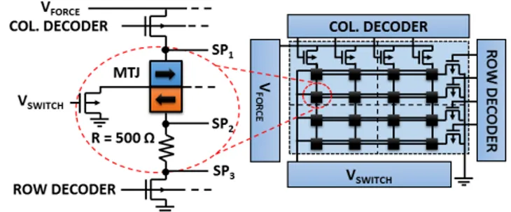
II. MEMORY ARCHITECTURE ANDEXPERIMENTAL SETUP The 1kbits memory device integrated into a CMOS process is made of a 32x32 array. The cell and the test array architec-ture are depicted in Fig. 1, where:
• MTJ is the Magnetic Tunnel Junction device, composed of two ferromagnetic layers separated by an insulating layer;
• SP1, SP2and SP3are sense pads used during read. SP1 is on the top of the MTJ, SP2 is connected right below
Fig. 1. Structure of a TAS-MRAM cell and its integration into the array tested in this work.
the MTJ and SP3is between a poly 500 Ω resistance and a select transistor.
In order to change the state of a memory cell, two different writing operations are available: Write ’0’ (W0) and Write ’1’ (W1). Both operations require two voltages: VF ORCE is required to locally heat the magnetic material, whereas VSW IT CH allows changing the magnetic field polarization after heating. All write operations have been performed with TF ORCE = 500ns, TSW IT CH = 600ns and Trise/f all = 500ns for both voltages in order to avoid overshoot issues. All read operations have been performed with VSW IT CH = 0V , VF ORCE= 0.3V , TF ORCE= 10µs and Trise/f all = 1µs.
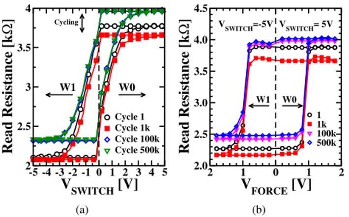
III. PARAMETER OPTIMIZATION IN FRESH DEVICES To evaluate the impact of heating and switching voltages on write operations, a preliminary hysteresis analysis of both pa-rameters has been performed on fresh devices.|VSW IT CH| has been increased from 0.2V to 5V with |∆VSW IT CH| = 0.2V and VF ORCE= 1.4V . The same procedure has been applied to evaluate VF ORCE hysteresis by increasing VF ORCE from 0.2V to 1.8V with ∆VF ORCE = 0.2V and |VSW IT CH| = 5V . A read operation has been performed after every step in both hysteresis analysis. Fig. 2 (a) shows the average resistances measured during switching voltage hysteresis and the switching parameters extracted for further analysis of W0 and W1 operations with VF ORCE = 1.4V :
• RW 0and RW 1are the average values of resistance RW 0 and RW 1, respectively measured at VSW IT CH = 5V and VSW IT CH= −5V .
© 2015 IEEE. Personal use of this material is permitted. Permission from IEEE must be obtained for all other uses, in any current or future media, including reprinting/republishing this material for advertising or promotional purposes, creating new collective works, for resale or redistribution to servers or lists, or reuse of any
copyrighted component of this work in other works.
This is the accepted version of the paper. The published version can be found at ieeexplore.ieee.org/document/7457476/ The DOI of the published version is: 10.1109/NVMTS.2015.7457476
-4 -2 0 2 4 VSWITCH [V] 2.0 2.5 3 3.5 4 Read Resistance [k Ω] <VW0> <VW1> ∆R ∆R <RW0> <RW1> (a) 2 1 0 1 2 V FORCE [V] 2.0 2.5 3.0 3.5 4.0 Read Resistance [k Ω] W1 W0 VSWITCH=-5V VSWITCH= 5V (b)
Fig. 2. Switching (a) and heating (b) voltage hysteresis measured on fresh devices. -5 -4 -3 -2 -1 0 1 2 3 4 5 V SWITCH [V] 2 2.5 3 3.5 4 Read Resistance [k Ω] W0 W1 Cycle 1 Cycle 1k Cycle 100k Cycle 500k Cycling (a) 2 1 0 1 2 V FORCE [V] 2.0 2.5 3.0 3.5 4.0 4.5 Read Resistance [k Ω] W1 W0 VSWITCH=-5V VSWITCH= 5V 1 1k 100k 500k (b)
Fig. 3. VSW I T CH hysteresis measured during W0 and W1 operations at
different cycles with VF ORCE= 1.4V (a). VF ORCE hysteresis measured
during W0 and W1 operations at different cycles with |VSW I T CH| = 5V
(b).
• VW 0 and VW 1 are the average switching voltages VW 0 and VW 1, respectively, that allow obtaining a variation ∆R = 1kΩ of the average measured resistance values. Fig. 2 (b) shows the average resistances of the array cells measured during heating voltage hysteresis in W0 and W1 operations with |VSW IT CH| = 5V . It can be observed that VF ORCE ≥ 1V is required in order to successfully switch the magnetic field, whereas using VF ORCE> 1.6V shows no advantages in terms of average resistance for both W0 and W1 operations. VF ORCE = 1.4V and |VSW IT CH| = 5V are shown to be the optimal write conditions, ensuring the highest resistance difference in W1 and W0 states.
IV. PARAMETER ANALYSIS UNDER CYCLING To evaluate the cells performance and reliability during cycling and the effect of the cell degradation, 500k W0 and W1 operations have been performed with VF ORCE = 1.4V and|VSW IT CH| = 5V .
Fig. 3 shows the switching voltage (a) and the heating volt-age (b) hysteresis evolution during cycling: an equal RW 0and RW 1 variation can be observed, thus keeping the resistance difference constant during cycling.
0 0.5 1 1.5 2 2.5 3 3.5 4 4.5 5
Read Resistance [KΩ]
0 10 20 30 40 50 60 70 80 90 100Cumulative Probability [%]
W1 W0Fig. 4. RW 0 and RW 1 cumulative probability functions measured during
500k cycling with VF ORCE= 1.4V ,|VSW I T CH| = 5V .
1 10 100 1k 10k 100k 500k
Switching Cycles
0 0.5 1 1.5 2 2.5 3 3.5 4 4.5Read Resistance [K
Ω]
<RW0> <RW1> VFORCE=1.2 V VFORCE=1.4 V VFORCE=1.6 V VFORCE=1.8 VFig. 5. RW 0 (full lines) and RW 1 (dotted lines) measured during 500k
cycling with different VF ORCE conditions.
Fig. 4 shows the cumulative distributions of the read re-sistances measured after W0 and W1 operations at different cycles. Left tails on the distributions appear during cycles due to the cell degradation for a limited percentage of cells (below 3% after 500k cycles).
In order to evaluate the impact of VF ORCE during cycling, 500k cycles have been performed with different VF ORCE values and |VSW IT CH| = 5V , measuring RW 0 and RW 1 at different cycles. RW 0 and RW 1 measured during cycling are reported in Fig. 5, showing a sudden cell degradation after 100k cycles with VF ORCE = 1.6V and after 1k cycles with VF ORCE = 1.8V , whereas the average resistances do not show any relevant change during the endurance tests with VF ORCE= 1.2V and 1.4V .
The dispersion coefficients (i.e. standard deviation over mean value) for RW 1and RW 0, evaluated during cycling with different VF ORCE conditions, are reported in Fig. 6: a rapid increase of their values can be observed before the breakdown with VF ORCE = 1.6V and VF ORCE = 1.8V at cycles 50k and 500, respectively. The use of VF ORCE = 1.4V induces the lowest cell-to-cell variability of RW 0 and RW 1 during cycling.
1 10 100 1k 10k 500k Switching Cycles 0.0 0.5 1.0 1.5 RW0 dispersion coeff.
CELLS BREAKDOWN LIMIT
(a) 1 10 100 1k 10k 500k Switching Cycles 0.0 0.5 1.0 1.5 R W1 dispersion coeff. VFORCE=1.2V VFORCE=1.4V VFORCE=1.6V VFORCE=1.8V CELLS BREAKDOWN LIMIT
(b)
Fig. 6. RW 0(a) and RW 1(b) dispersion coefficients measured during 500k
cycling with different VF ORCE conditions.
0 1 2 3 4 5 VW0,W1 [V] @ VFORCE=1.2V 0 256 512 768 1k
Cumulative number of cells
V W0 VW1 1 1k 100k 500k 0 1 2 3 4 5 VW0,W1 [V] @ VFORCE=1.4V 0 256 512 768 1k
Cumulative number of cells
V W0 V W1 1 1k 100k 500k 0 1 2 3 4 5 VW0,W1 [V] @ VFORCE=1.6V 0 256 512 768 1k
Cumulative number of cells
V W0 V W1 1 1k 100k 0 1 2 3 4 5 VW0,W1 [V] @ VFORCE=1.8V 0 256 512 768 1k
Cumulative number of cells
1 1k VW0 V
W1
Fig. 7. Cumulative number of switching cells reaching the assumed variation ∆R = 1kΩ with different VF ORCEduring cycling.
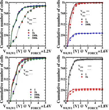
The cumulative distributions of the VW 0 and VW 1 pa-rameters measured during cycling with different VF ORCE conditions are reported in Fig. 7. The cumulative number of cells do not reach 1k because a limited number of cells do not reach, in switching, the assumed ∆R = 1kΩ. The minimum cell-to-cell variability during the endurance test is obtained by using VF ORCE = 1.4V . Moreover, VF ORCE = 1.4V shows the highest cumulative number of switched cells: this means that a higher cells percentage reached the requested resistance variation ∆R = 1kΩ. According to the obtained results, the use of VF ORCE= 1.4V has to be preferred since it guarantees the best reliability in cycling, denoted as the percentage of cells correctly switching. Using higher heating voltages results in a reduced yield (lower percentages of cells reaching the
0 2 4 100 102 104 106 0 2 4 Cycle VFORCE = 1.2 V VSWITCH [V] R W 0 [ kΩ ] 0 2 4 100 102 104 106 0 2 4 Cycle VFORCE = 1.4 V VSWITCH [V] R W 0 [ kΩ ] 0 2 4 100 102 104 106 0 2 4 Cycle VFORCE = 1.6 V VSWITCH [V] R W 0 [ kΩ ] 0 2 4 100 102 104 106 0 2 4 Cycle VFORCE = 1.8 V VSWITCH [V] R W 0 [ kΩ ]
Fig. 8. 3D plot of RW 0as a function of VSW I T CH and cycle number for
different VF ORCE conditions.
0 2 4 100 10 2 104 106 0 2 4 Cycle VFORCE = 1.2 V VSWITCH [V] R W 1 [ kΩ ] 0 2 4 100 10 2 104 10 6 0 2 4 Cycle VFORCE = 1.4 V VSWITCH [V] RW 1 [ kΩ ] 0 2 4 100 102 104 106 0 2 4 Cycle VFORCE = 1.6 V VSWITCH [V] R W 1 [ kΩ ] 0 2 4 100 102 10 4 106 0 2 4 Cycle VFORCE = 1.8 V VSWITCH [V] R W 1 [ kΩ ]
Fig. 9. 3D plot of RW 1as a function of VSW I T CH and cycle number for
different VF ORCE conditions.
requested ∆R) and in a faster breakdown. According to the reported analysis, RW 0 and RW 1 are shown to depend on VF ORCE, VSW IT CH and cycling: the relationship between these parameters has been analyzed through 3D plots for different VF ORCE conditions for both W0 (Fig. 8) and W1 (Fig. 9). RW 0and RW 1depend on|VSW IT CH| for any cycling and VF ORCE conditions:|VSW IT CH| = 5V allows obtaining the highest RW 0 values and lowest RW 1 values. Using too high heating voltages (i.e. VF ORCE ≥ 1.6V ) results in a shorter lifetime, independently from VSW IT CH.
The most important parameter used to evaluate the switch-ing capabilities on MRAM is the tunnel magnetoresistance (TMR) [12], calculated as:
T M R = RW 0− RW 1
RW 1 (1)
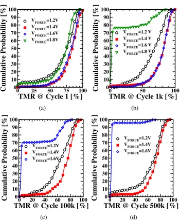
TMR cumulative distributions measured during endurance test at different cycles are reported in Fig. 10 for each VF ORCE condition. Since TMR depends on the difference between RW 0 and RW 1 and the resistance shift due to cell degradation is the same on both resistive states, no relevant variations can be observed on TMR until the cell breakdown is reached. VF ORCE = 1.4 allows obtaining the highest TMR in each cycling condition.
0 25 50 75 100 TMR @ Cycle 1 [%] 0 10 20 30 40 50 60 70 80 90 100 Cumulative Probability [%] V FORCE=1.2V VFORCE=1.4V V FORCE=1.6V V FORCE=1.8V (a) 0 50 100 TMR @ Cycle 1k [%] 0 10 20 30 40 50 60 70 80 90 100 Cumulative Probability [%] VFORCE=1.2 V VFORCE=1.4 V V FORCE=1.6 V VFORCE=1.8 V (b) 0 20 40 60 80 100 TMR @ Cycle 100k [%] 0 10 20 30 40 50 60 70 80 90 100 Cumulative Probability [%] VFORCE=1.2V V FORCE=1.4V VFORCE=1.6V (c) 0 20 40 60 80 100 TMR @ Cycle 500k [%] 0 10 20 30 40 50 60 70 80 90 100 Cumulative Probability [%] VFORCE=1.2V V FORCE=1.4V VFORCE=1.6V (d)
Fig. 10. TMR measured during cycling with different VF ORCEconditions
at cycle 1 (a), 1k (b), 100k (c) and 500k (d) .
V. CONCLUSIONS
The cell-to-cell variability and the switching reliability evolution during cycling have been evaluated on 1kbits TAS-MRAM. Both cell-to-cell variability and switching reliability depend on the chosen switching voltages. The relationship among characteristic switching parameters and operating con-ditions have been thoroughly investigated.
ACKNOWLEDGMENTS
The research leading to these results has (partially) received funding from the European Community’s Seventh Framework Programme FP7 under grant agreement n 619246.
REFERENCES
[1] W. Gallagher, D. Abraham, S. Assefa, S. Brown, J. DeBrosse, M. Gaidis, E. Galligan, E. Gow, B. Hughes, J. Hummel, S. Kanakasabapathy, C. Kaiser, M. Lamorey, T. Maffit, K. Milkove, Y. Lu, J. Nowak, P. Rice, M. Samant, E. O’Sullivan, S. Parkin, R. Robertazzi, P. Trouilloud, D. Worledge, G. Wright, and S.-H. Yang, “Recent advances in MRAM technology,” in IEEE VLSI-TSA Int. Symp., April 2005, pp. 72–73. [2] S. Senni, L. Torres, G. Sassatelli, A. Bukto, and B. Mussard, “Power
efficient thermally assisted switching magnetic memory based memory systems,” in Inter. Symp. on Reconfigurable and Communication-Centric
Systems-on-Chip (ReCoSoC), May 2014, pp. 1–6.
[3] R. Sousa, I. Prejbeanu, D. Stanescu, B. Rodmacq, O. Redon, B. Dieny, J. Wang, and P. Freitas, “Tunneling hot spots and heating in magnetic tunnel junctions,” J. of App. Phys., vol. 95, pp. 6783–6785, 2004. [4] J. Azevedo, A. Virazel, A. Bosio, L. Dilillo, P. Girard, A. Todri-Sanial,
J. Alvarez-Herault, and K. Mackay, “A complete resistive-open defect analysis for thermally assisted switching MRAMs,” IEEE Trans. on Very
Large Scale Integration (VLSI) Systems, vol. 22, pp. 2326–2335, Nov 2014.
[5] I. Prejbeanu, S. Bandiera, J. Alvarez-H´erault, R. Sousa, B. Dieny, and J. Nozi`eres, “Thermally assisted MRAMs: ultimate scalability and logic functionalities,” Journal of Physics D: Applied Physics, vol. 46, no. 7, p. 074002, 2013.
[6] I. Prejbeanu, W. Kula, K. Ounadjela, R. Sousa, O. Redon, B. Dieny, and J.-P. Nozieres, “Thermally assisted switching in exchange-biased storage layer magnetic tunnel junctions,” IEEE Trans. on Magnetics, vol. 40, pp. 2625–2627, 2004.
[7] I. Prejbeanu, M. Kerekes, , R. Sousa, H. Sibuet, O. Redon, B. Dieny, and J.-P. Nozieres, “Thermally assisted MRAM,” J. Phys.: Condens. Matter, vol. 19, pp. 165 218–165 241, 2007.
[8] S. Chaudhuri, W. Zhao, J.-O. Klein, C. Chappert, and P. Mazoyer, “De-sign of TAS-MRAM prototype for NV embedded memory applications,” in IEEE Int. Memory Workshop (IMW), May 2010, pp. 1–4.
[9] R. Ferreira, S. Cardoso, and P. Freitas, “Dynamic thermo-magnetic writing in tunnel junction cells incorporating two GeSbTe thermal barriers,” in IEEE Int. Magnetics Conf., May 2006, pp. 394–394. [10] J. Azevedo, A. Virazel, A. Cheng, A. Bosio, L. Dilillo, P. Girard,
A. Todri, and J. Alvarez-Herault, “Performance characterization of TAS-MRAM architectures in presence of capacitive defects,” in Int. Conf. on
Advances in System Testing and Validation Lifecycle, Oct 2013, pp. 39– 44.
[11] A. Grossi, C. Zambelli, P. Olivo, P. Pellati, M. Ramponi, J. Alvarez-Herault, and K. Mackay, “Automated characterization of TAS-MRAM test arrays,” in IEEE Int. Conference on Design Technology of Integrated
Systems in Nanoscale Era (DTIS), April 2015, pp. 1–2.
[12] S. Yuasa, A. Fukushima, K. Yakushiji, T. Nozaki, M. Konoto, H. Mae-hara, H. Kubota, T. Taniguchi, H. Arai, H. Imamura, K. Ando, Y. Shiota, F. Bonell, Y. Suzuki, N. Shimomura, E. Kitagawa, J. Ito, S. Fujita, K. Abe, K. Nomura, H. Noguchi, and H. Yoda, “Future prospects of MRAM technologies,” in IEEE Int. Electron Devices Meeting (IEDM), Dec 2013, pp. 3.1.1–3.1.4.