Ultrafast spectro-microscopy of
highly excited low dimensional
materials
Alessandra Virga
A Thesis presented for the degree of
Doctor of Philosophy
Femtoscopy Group (Prof. T. Scopigno)
Department of Physics
University Sapienza
Italy
Ultrafast spectro-microscopy of highly excited low
dimensional materials
Alessandra Virga
Submitted for the degree of Doctor of Philosophy
December 2018
Abstract
Born-Oppenheimer approximation (ABO) is the assumption that the motion of atomic nuclei and electrons in molecules can be separated and independently treated. In solids, ABO is well justified when the energy gap between ground and excited electronic states is larger than the energy scale of the nuclear motion. Graphene represents a notable exception of this acceptantance. In particular, here we unravel the key role of the gapless linear Dirac dispersion in the vibrational Raman response of the system in the case of impulsively photoexcited graphene.
First, we unambiguously describe Four-Wave Mixing (FWM) processes in graphene, which depend on the resonant nature of the electronic interactions. Indeed, the over-all spectral response is described in terms of a third order diagrammatic description of the light-matter interaction. We disclose that the interference between Coherent anti-Stokes Raman Scattering (CARS) and Non-Vibrationally Resonant Background (NVRB) generates Lorentzian dip spectral profiles. Actually, by introducing an ex-perimental time delayed FWM scheme, able to modify the relative strength of the two contributions, we observe the first evidence of CARS peak equivalent to the Raman spectrum in graphene.
Second, we adopt sub picosecond photoexcitation which impulsively localize en-ergy into graphene electronic subsystem. While the response of hot charge carriers is well-characterized, unraveling the behavior of optical phonons under strongly out-of-equilibrium conditions remains a challenge. Using a 3-ps laser excitation, which trades off between impulsive stimulation and spectral resolution, we show how the Raman response of graphene can be detected in presence of an electronic subsystem temperature largely exceeding that of the phonon bath. We find a peculiar behaviour
iii
of the period and lifetime of both the G and 2D phonons as function of the carriers temperature in the range 1700-3100 K, suggesting a broadening of the Dirac cones. Accordingly, we reconsider the traditional scenario of the electron-phonon scattering in a highly excited transient regime.
List of publications/conference contributions
This thesis is based on following publications in journals and conference contri-butions:
C. Ferrante, G. Batignani, G. Fumero, E. Pontecorvo, A. Virga, L. C. Mon-temiglio, G. Cerullo, M. H. Vos, T. Scopigno. Resonant Broadband Stimulated Raman scattering in Myoglobin, Journal of Raman Spectroscopy, 2018; 18,
10.1002/jrs.5323
C. Ferrante, A. Virga, L. Benfatto, M. Martinati, D. De Fazio, U. Sassi, C. Fasolato, A.K. Ott, P. Postorino, D.Yoon, G. Cerullo, F. Mauri, A. C. Ferrari, T. Scopigno. Raman spectroscopy of graphene under ultrafast laser excitation, Nature
Communications, (2018) 9:308, 10.1038/s41467-017-02508-x
A. Virga, C. Ferrante, L. Benfatto, M. Martinati, D. De Fazio, U. Sassi, C.
Fasolato, A.K. Ott, P. Postorino, D.Yoon, G. Cerullo, F. Mauri, A. C. Ferrari, T. Scopigno. The Raman spectrum of Graphene in presence of highly excited charge
carriers, Oral Contribution, Graphene2017.
A. Virga, C. Ferrante, L. Benfatto, M. Martinati, D. De Fazio, U. Sassi, C.
Fasolato, A.K. Ott, P. Postorino, D.Yoon, G. Cerullo, F. Mauri, A. C. Ferrari, T. Scopigno. Phonon anomalies in Graphene induced by highly excited charge carriers, Oral Contribution, CLEO/Europe-EQEC 2017 Conference on Lasers and
Electro-Optics Europe & European Quantum Electronics Conference. A. Virga, C. Ferrante, L. Benfatto, M. Martinati, D. De Fazio, U. Sassi, C.
Fasolato, A.K. Ott, P. Postorino, D.Yoon, G. Cerullo, F. Mauri, A. C. Ferrari, T. Scopigno. The role of electron-phonon scattering in the Raman spectrum of Graphene in presence of highly excited charge carriers, Oral Contribution,
Fis-v Mat2017 - The Italian National Conference on Condensed Matter Physics. A. Virga, C. Ferrante, L. Benfatto, M. Martinati, D. De Fazio, U. Sassi, C.
Fasolato, A.K. Ott, P. Postorino, D.Yoon, G. Cerullo, F. Mauri, A. C. Ferrari, T. Scopigno. Raman spectroscopy of graphene under ultrafast laser excitation, Oral
Contribution, UP2018 XXI International Conference on Ultrafast Phe-nomena.
A. Virga, C. Ferrante, L. Benfatto, M. Martinati, D. De Fazio, U. Sassi, C.
Fasolato, A.K. Ott, P. Postorino, D.Yoon, G. Cerullo, F. Mauri, A. C. Ferrari, T. Scopigno. Out of equilibrium electron-phonon interaction in graphene unraveled
by Raman scattering by picosecond excitation, Poster Presentation, ICORS2018
Contents
Abstract ii
List of publications/conference contributions iv
1 Motivation 1
Part I: Introduction 5 2 Graphene and its Raman spectrum 6
2.1 Structural properties: from graphite to graphene . . . 6
2.2 Electronic properties in graphene . . . 8
2.3 Lattice vibrations in graphene . . . 12
2.4 Optical properties . . . 14
2.5 Ultrafast dynamics in graphene . . . 19
2.6 Raman Spectroscopy . . . 23
2.6.1 Classical picture of light scattering . . . 24
2.6.2 The quantum description . . . 28
2.7 Raman spectroscopy in graphene . . . 31
2.8 Beyond graphene: towards heterostructures-based devices . . . 36
Part II: Results 39 3 Narrowband CARS in graphene 40 3.1 A brief roadmap towards Coherent Raman Microscopy . . . 41
3.2 Ultrashort pulse propagation . . . 44
3.2.1 Four-wave mixing . . . 47 vi
Contents vii
3.3 Coherent anti-Stokes Raman Scattering (CARS) . . . 49
3.4 Light-matter interaction: a semi-classical approach . . . 51
3.4.1 Density matrix . . . 53
3.4.2 Interaction picture . . . 54
3.5 Nonlinear Polarization . . . 56
3.5.1 Third-order interaction . . . 59
3.6 Diagrammatic approach in CARS . . . 61
3.7 SLG third-order nonlinear response . . . 66
3.8 Experimental methods . . . 68
3.8.1 Development of CARS microscopy . . . 68
3.8.2 Generation of pulses . . . 70
3.8.3 The fiber-laser source . . . 72
3.9 Experimental setup . . . 74
3.9.1 Graphene sample and CW Raman Characterization . . . 81
3.10 Time-delayed CARS . . . 82
3.11 Resonant CARS in graphene: a diagrammatic approach . . . 85
3.12 CARS Imaging . . . 88
4 Pulsed Spontaneous Raman spectroscopy in graphene 93 4.1 T-dependent Raman spectroscopy in graphene: a review . . . 94
4.1.1 Theoretical description of the e-ph coupling . . . 96
4.2 Experimental methods . . . 101
4.2.1 Pulsed Raman setup . . . 101
4.2.2 CW Raman setup . . . 102
4.3 Continuous-wave Raman spectroscopy in SLG . . . 103
4.4 Pulsed Raman spectroscopy in SLG . . . 106
4.5 Model . . . 113
5 Conclusions 121
Bibliography 124
Contents viii
List of Tables 158
Appendix 160
Chapter 1
Motivation
Over the last decade the field of material sciences has witnessed significant increase in the fabrication of systems with reduced dimensionality. It is now understood that these materials on sufficiently short length scales exhibit properties that are consid-erably different from the bulk materials. Graphene is an example of this tendency: it is a one-atom thick planar sheet of sp2 bonded carbon atoms, that are packed in a
honeycomb crystal lattice. Even if it was isolated only in 2004 [1], since then it has been the focus of research activities in view of its great potential to underpin new disruptive technologies, substituting materials used in existing applications but also leading to radically new devices [2]. This growing interest has culminated in the recognition of graphene as one of the two pillars, that lead and inspire the projects launched in EU Horizon 2020 programme. Several recent results highlight the ver-satility in the application of this system, ranging from solar cells and light-emitting devices to touch screens, photodetectors and ultrafast lasers [3]. Nowadays, even global industrial partners, as Samsung, are working together with researchers and universities to create a new technology that promises double the electric capacity of Lithium batteries, thanks to the introduction of graphene as an efficient energy storage solution [4, 5]. Clearly all these applications are related to unique proper-ties, such as high mobility, optical transparency and high termal conductivity [6–8], in addition to flexibility, robustness, and environmental stability [2, 5]. The very origin of such properties is strictly related to the gapless linear energy dispersion of graphene and the breakdown of the Born-Oppenheimer [9] approximation which
Chapter 1. Motivation 2
determines a strong coupling between electronic and vibrational degrees of freedom in the system.
Such peculiar properties obviously influence the light-matter interaction in graphene, making it a promising material for many optoelectronics devices due to a fast response time and a notable broadband wavelength-independent absorptive ten-dency [3, 7]. In particular, these features depend on the ultrafast dynamics of the system, which has aroused great interest in the last decade to be studied by means of time-resolved techniques [10, 11]. These studies have disclosed the key role of the carriers relaxation channels and, among them, the importance of phononic chan-nel, which can be precisely observed by means of Spontaneous Raman (SR) Spec-troscopy [12]. This frequency-domain technique provides information about the energy and dephasing time of phonons at thermodynamic equilibrium. This latter quantity is related to the inverse of Raman linewidth, although disentangling the specific processes that generate homogeneous and heterogeneous broadening in the frequency domain is a challenge.
For this purpose, in 2013, within the context of my master thesis, I embraced a project aimed at examining the graphene lifetime in time domain by detecting coherent Raman processes [13], wherein a short (tens of fs) pulse induces atoms to oscillate in phase, i.e. coherently, and a second time-delayed (ps) pulse probes the Raman spectrum. According to these measurements, the G-phonon dephasing time was about 5 times less than expected from the frequency-domain techniques [12]. Although a few possible explanation could be found, the full understanding of the data were not achived at the end of the work.
Is this effect due to the coherent feature of the photoexcited phonons? Could it be related to thermic effects? Could it be due to the use of pulsed excitation in the experiment instead of the continuous-wave lasers involved in Spontaneous Raman spectroscopy?
These open questions contributed to motivate this Ph.D. thesis. In this project, I combined coherent Raman techniques and picosecond Spontaneous Raman aiming at a complete characterization of graphene out-of-equilibrium electronic and vibrational degrees of freedom. In particular, we first analyze much more in detail the nature
Chapter 1. Motivation 3
of coherent Raman process in graphene. Then, we perform a Spontaneous Raman experiment by means of a picosecond laser pulses in order to isolate the effect of ultrafast optical excitation.
This work aims for bridging the gap between the graphene scientific community and the non-linear Raman spectroscopy one. The thesis is structured in five Chapters which summarize the main theoretical and experimental work done during my Ph.D. studies.
In Chapter One, the motivations of this Ph.D. thesis are presented and contex-tualized.
Chapter Two is introductive and sets the theoretical grounds for rest of the Chapters. In particular this Chapter discusses the main physical aspects of graphene, including electronic, vibrational and optical properties. Moreover, we introduce the main mechanisms responsible for the light-matter interaction with this system. An introduction to Spontaneous Raman spectroscopy is given, focusing on the graphene Raman response as fundamental characterization tool.
Chapter Three is totally focused on the CARS response in graphene. In par-ticular, this section discusses about the derivation of four coupled equations for four-wave mixing process derived from Maxwell’s equations. Then, a semiclassical treatment based on Feynman diagrams is presented. The rest of the chapter is focused on the experimental results. The compact versatile fiber-format Coherent Raman microscopy setup developed in our laboratory and its time-delayed scheme are discussed. CARS response of graphene is presented and it is theoretically de-scribed in terms of a quantum modelization of the third order polarization.
In Chapter Four, electron-phonon scattering, along with anharmonicity, are dis-cussed due to ther pivotal role in the description of the equilibrium phonon properties in graphene studied by means of Raman scattering. In particular, an extensive de-scription of e-ph coupling is presented in terms of Green’s function and self-enegy. Moreover, spontaneous Raman measurements in graphene by using a 3-ps laser pulses are performed; indeed we show how the Raman response of graphene can be detected in presence of an electronic subsystem temperature largely exceeding that of the phonon bath. The experimental data are modelled by reconsidering
Chapter 1. Motivation 4
the traditional scenario of the electron-phonon scattering in a highly excited tran-sient regime, wherein graphene is in out-of-equilibrium condition photoinduced by ps-pulses involved in the experiment.
Chapter Five is equivalent to a brief summary of the main results of this thesis. Finally, details on CARS interaction are provided in the appendix.
Chapter 2
Graphene and its Raman
spectrum
The key role of carbon atoms in all organic and live organisms is absolute; however for long time only two structures, diamond and graphite [14], were commonly used. A new era for carbon has begun since the advent of fullerene in 1985 [15] and car-bon nanotubes in 1991 [16]. Only in 2004 [17] the cornerstone of their structure, graphene, a single layer of carbon atoms bounded in sp2 configuration forming an
hexagonal lattice, was finally isolated and stable by itself. This has awaked inter-est on researches for this new carbon form, paving the way for the success of low-dimensional materials in several fields, from optoelectronics [2] to spintronics [18]. In this chapter, the main properties of graphene are reviewed. In addition, it is given a brief introduction to Raman effect, at the base of the spectroscopic tech-niques performed in this work. In particular, it is focused on the Raman spectrum of graphene.
2.1
Structural properties: from graphite to graphene
Graphene is a one-atom thick planar sheet of sp2 bonded carbon atoms [1, 8, 17]. These atoms are packed in a honeycomb crystal lattice; it is actually an hexagonal lattice with a basis of two ions in each unit cell. Stacking of these graphene sheets forms multilayer graphene and graphite. Although there exist many different
2.1. Structural properties: from graphite to graphene 7
Figure 2.1: Unit-cell convention in single layer graphene. (a) Honeycomb lattice: The vectors δ1, δ2, and δ3connect the nearest carbon atoms, separated by a distance
aCC ∼ 1.42 ˚A. The vectors a1 and a2 are basis vectors of the triangular Bravais
lattice. A and B sublattice atoms are represented in blue and red, respectively. (b) Reciprocal lattice of the triangular lattice. The vectors b1 and b2 are basis vectors
of the reciprocal lattice.
ing configurations, the lowest energy stacking forms when two adjacent layers are rotated by 60o relative to each other and it is called Bernal stacking. The distance between graphene sheets in Bernal graphite is 3.35 ˚A in the z-direction.
Referring to the honeycomb crystal lattice shown in Fig.2.1.a, if aCC ∼ 1.42 ˚A is
the distance between the nearest neighbors, we identify the basic unit cell through the vectors: a1 = aCC 2 (3, √ 3), a2 = aCC 2 (3,− √ 3) Accordingly, the nearest neighbors are identified by the vectors:
δ1 =−
1
3(a1+ a2), δ2 = δ1+ a1, δ3 = δ1+ a2 The reciprocal unit cell, shown in Fig.2.1.b, has basic vectors:
b1 = 2π 3aCC (1,√3), b2 = 2π 3aCC (1,−√3)
2.2. Electronic properties in graphene 8
Graphene honeycomb lattice was firstly isolated in 2004 [17] by micromechanical cleavage from graphite [1]. This procedure consists in peeling off a piece of graphite by means of an adhesive tape. Although the production technology has rapidly strenghten [19], this is still the method mainly chosen for fundamental research, as it guarantees the best samples in terms of purity, defects, mobility and optoelectron-ics properties. Nevertheless, it is impractical for large scale applications. Indeed, the widespread of graphene in technological application requires the production of large scale assembly with controlled growth. At this aim, several techniques have been developed [19]. Chemical vapour deposition [20] is able to produce few-layers graphene (FLG) on various substrates by feeding hydrocarbons at a suitable temper-ature [21–23], but it is not suitable for obtaining single layer graphene (SLG). Liquid phase exfoliation of graphite consists in chemical wet dispersion followed by ultra-sonication, both in aqueous and non-aqueous solvents [24, 25]. This method offers advantages of scalability and no requirement of expensive growth substrates. Other remarkable techniques include the chemical synthesis [26] and carbon segregation from silicon carbide or metal substrates [27, 28].
2.2
Electronic properties in graphene
In graphene, each carbon atom has three in-plane σ bonds and one out-of-plane 2pz
orbital. The σ band, related to planar sp2orbitals, yields strong covalent bonds with
the nearest carbon atoms; the π orbitals exhibit interlayer overlap in graphite that accounts for weak bonding along with van der Waals forces between the graphene layers. Thus, interaction between adjacent graphene layers or even interactions between a graphene layer and the substrate should affect the electronic structure [1, 8, 14].
Since there is no overlap between σ and π orbitals, in theoretical analysis as tight-binding method, each band can be treated independently from the others. The shortest gap between conduction and valance band is associated to σ band at Γ point: it counts more than 10 eV, revealing a covalent behavior of the sp2 bonds.
2.2. Electronic properties in graphene 9
points, showing a linear energy dispersion [8]. Since there is one valence electron per carbon atom in graphene, the valence band is completely filled, while the conduction band is completely empty: for this reason, graphene can be described as a zero-gap semiconductor.
As the number of layers increases, the energy dispersion becomes parabolic at the K point and the opening of a gap takes place due to interaction between different sheets and symmetry breaking. This justifies a semi-metallic behaviour [29].
Tight-binding method is able to calculate the spectrum of non-interacting elec-trons in this material. Here we restrict ourselves to the case of the nearest-neighbor tunneling terms and the most important features of the spectrum are well-described. We directly work in second quantization and define the annihilation (creation) op-erators of an electron at the lowest orbital centered around atoms of sublattice A and B (see Fig.2.1): a, b, (a†, b†) .
The full tight-binding Hamiltonian of graphene is given by [30, 31]:
H =−t∑
n,δ,σ
(a†n,σbn+δ,σ+ c.c.) (2.2.1)
This expression indicates that the δ vectors connect the A atoms to their nearest neighbors and that the hopping, quantified by the parameter t, is possible only between the two different sublattices. In the equation, c.c stands for complex conju-gate. In the following, the sublattice index will play the role of a pseudospin (σ is the real spin index) and the model can be expressed in terms of a spinor Ψ†= (a†k, b†k), where the operators a†k and b†k indicate the excitations on the A and B sublattices in the k-space.
First of all, we want to diagonalize the Hamiltonian in order to determine its eigenvalues [31]. Since we have a translation invariant system, we now go to Fourier space and write:
a†n,σ = √1 N ∑ k e−ik·rna† k,σ
By substituting this expression in Eq.2.2.1, we can rewrite the Hamiltonian out as:
H =−t∑
k,δ,σ
e−ik·δa†(k)b(k) + h.c. =∑
δ,σ
2.2. Electronic properties in graphene 10
where the matrix h, called the Bloch Hamiltonian, takes the form:
h = 0 f (k) f∗(k) 0 (2.2.3) with f (k) =−t∑ δ e−ik·δ =−t ( e−ikxaCC + 2eikxaCC/2cos ( kyaCC √ 3 2 )) . Since h is an Hermitian matrix, the diagolization is guaranteed and the corresponding eigenvalues are given by:
ϵ±=±|f(k)| = ±t √
3 + 2 cos(√3kyaCC) + 4 cos( √
3kyaCC/2) cos(3kxaCC/2)
Notice that even this simple tight-binding model predicts that the two bands touch at some points in the first Brillouin zone. By taking spin into account, we get that the lower band is exactly filled, since graphene has one accessible electron per atom,. This means that if we now discuss small excitations above the ground state, the excitations to be considered are those near the crossing points. To write the low energy theory, we have therefore to identify these points. We get them from the condition f (k) = 0. This equation gives us the following points (plus any reciprocal lattice vector): ( 0,± 4π 3√3aCC ) ,± 2π 3aCC ( 1,√1 3 ) , ± 2π 3aCC ( 1,−√1 3 )
Actually, all the points listed above sit in the corners of the first Brillouin zone. A simple inspection shows that the above set of k-space vectors is not independent and we choose one representative vector from each set. These are conventionally called
K and K′: K = 2π 3aCC ( 1,√1 3 ) , K′ = 2π 3aCC ( 1,−√1 3 ) (2.2.4) The energy bands cross at these points, and the gap closes. In order to study the low-energy excitation regime, we expand around K and K′:
f (K′+ q)≈ −3taCC 2 e
−2πi/3(q
y+ iqx)
Thus, upon changing the phases of A and B, which physically means changing the phases of the basis wavefunctions, the h matrix can be brought to the form:
h(K′+ q) =−3taCC 2 0 qy+ iqx qy− iqx 0 = −~vFq· σ (2.2.5)
2.2. Electronic properties in graphene 11
where σ is the vector of Pauli-matrices. This is just the 2D massless Dirac Hamil-tonian, which describes free relativistic electrons, where the light speed has been replaced by the Fermi velocity vF = 3ta2CC~ ∼ 106 m/s. Keeping the same notation
and using the same spinor, the Hamiltonian around K would give instead:
h(K + q) =~vFq· σ (2.2.6)
The eingenvalues of this matrix are:
E =±~vFq (2.2.7)
Then, around K and K′ the energy dispersion is linear (see Fig.2.2 and, more im-portantly, we can have both positive and negative excitations (i.e. electrons and holes), described by the same Hamiltonian (charge conjugation). Notably in sup-ported graphene, many body effects can be neglected, i.e. electrons behave as if there were no electron-electron interactions [32–34]. As a result, vF can be
consid-ered as a constant. If now we consider the expansion up to the second order in
k we retrieve the so-called trigonal warping [8]. For higher energy states the cone
deforms to adopt a triangular-like shape, i.e. the dispersion relation depends on the direction in momentum space. This effect is neglected in this work.
Eq.2.2.7 strongly recalls the photons dispersion relation, as it can be expressed in the relativistic form:
E(q) =±√q2c2
∗+ m2∗c4∗ =±c∗q
with an effective mass m∗ = 0 and an effective light velocity c∗equal to the Fermi ve-locity vF. For this reason, electrons and holes in graphene are called massless Dirac
fermions [8]. Nevertheless, electrons in graphene are not strictly speaking relativistic as their velocity is approximately 300 times smaller than the light velocity, the elec-tronic wavefunctions near the K and K points obey the Dirac equation (and not the Schr¨odinger one) for massless fermions and have a well defined chiralityTIR,Noselov. We now calculate the electronic density of states g(E), which counts the number of quantum states in the vicinity of a fixed energy E [35]. It may be obtained from the total number of states N below the energy E.
N (E) = d∑ ϵ<E = A ∫ E 0 dϵ g(ϵ) (2.2.8)
2.3. Lattice vibrations in graphene 12
Figure 2.2: The band structure in graphene: ARPES measurement of the dispersion relation of epitaxial graphene (from Ref. [36])
So, g(E)can be expressed as:
g(E) = 1
A ∂N
∂E (2.2.9)
where A is the total surface and d = 4 takes into account the degeneracy due to internal degrees of freedom (valley degeneracy and electron spin). In the vicinity of the Dirac points, N may be calculated quite easily because of the isotropy of the energy dispersion. N (E) = Ad 2π ∫ q(E) 0 dq q (2.2.10)
Then, it follows the expression for g(E):
g(E) = d 2π = q(E) ∂E/∂q = 2 π E ~2v2 F
wherein the spin and the valley degeneracy are taken into account. Note that due to the electron-hole symmetry, g(E) is valid for both electrons and holes. It scales linearly with the energy E and vanishes at the Dirac points. This situation is different from what is usually happening in a solid, where the density of states is constant (due to the parabolic dispersion relation).
2.3
Lattice vibrations in graphene
Graphene has two atoms for unit cell. Then there are six possible phonon dis-persion branches in Γ point at Brillouin zone (see Fig. 2.3): three optical (O), whose frequencies do not vanish in the long-wavelength limit, and three acoustic (A). The vibrations perpendicular to the plane formed by graphene lattice (out-of-plane modes) are softer than in-plane motions; the latter can be distinguished
2.3. Lattice vibrations in graphene 13
between longitudinal and transverse, with respect to the vector formed between the two carbon atoms that compose the unit cell. So the six branches can be divided into three cases: two in-plane longitudinal (iLA and iLO), two in-plane transverse (iTA and iTO) and two out-of-plane transverse (oTA and oTO) [37].
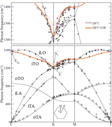
These six branches can be measured experimentally by inelastic neutron [38] or X-ray [39–41] scattering, as well as electron energy loss spectroscopy (EELS) [42, 43]. Raman scattering can also be performed to study the phonon modes in graphene as it will appear clear in the following sections. From a theoretical point of view, the phonon dispersion has been determined using empirical force-constant calculations [38, 41] and density functional theory (DFT) [39, 44–46]. In order to reproduce the experimental results, graphene case requires to consider contributions from long-distance forces, such as from the n-th neighbor atoms, (n = 1, 2, 3, 4...). These effects are taken into account by the so-called GW method [47, 48]. Other correction in the calculations are given by renormalization effects [49] or the electron-phonon coupling (EPC), a process in which a electron-phonon can create an electron-hole pair. This intense EPC cannot be understood within the framework of the Born-Oppenheimer approximation [9] and gives rise to an interesting effect, known as Kohn anomaly [48].
Indeed, in the phonon dispersion curve, shown in Fig. 2.3, the most remarkable feature is the discontinuity in the frequency derivative of the highest optical branches at Γ and at K, corresponding to E2g and A′1 points respectively. This feature can be
explained by Kohn anomalies. In fact, in semimetallic systems the atomic vibrations are partially screened by electrons: this can occur only for phonons, whose wavevec-tor could connect two electronic states at the Fermi surface. As in graphene, the band gap is zero only at two equivalent points K and K’=2K, Kohn anomalies will appear only in Γ and K points at Brillouin zone. They cause a strong interaction between electron and phonons, that makes E2g and A′1 symmetry points responsible
for the main features of Raman spectrum of graphene [50].
Among the six normal modes (two doubly degenerate), the in-plane optical E2g
phonon is the only Raman active mode: it is due to the in-plane streching of carbon-carbon bonding and it gives rise to the G band, which is signature of all sp2 carbon
2.4. Optical properties 14
Figure 2.3: Experimental and simulated phonon dispersion of graphene. The solid lines represent DFT calculations with GW corrections from Refs. [40, 47]. The sym-bols represent inelastic X-ray scattering measurements from Refs. [39] (full circles) and [41] (open triangles). The six phonon branches are labeled. (Adapted from Ref. [48]).
allotropes [51]. The A′1 vibration mode corresponds to the breathing modes of six-atom rings and requires a defect for its activation: thus it is prohibited in pris-tine graphene. As the number of graphene sheets increases progressively towards graphite, the two atoms of the unit cell in each layer are no more equivalent. In fact graphite has four atoms per unit cell and all the optical modes become Davydov-doublets. It follows that there are two Raman active E2g modes in graphite, each
doubly degenerate [12].
2.4
Optical properties
Graphene has unprecedented thermoelectrical characteristics: high electrical con-ductivity (∼ 1.0 · 108S/m), high melting point (4510 K), high thermal conductivity
2.4. Optical properties 15
(2000−4000 W m−1K−1, 5000 W/m K), highest current density (∼ 1.6·109A/cm2), including a high electron mobility (200000 cm2V−1 s−1 at electron density ∼ 2 ·
1011cm−2) [5, 8, 52, 53]. In particular, in this section, we discuss more in detail the peculiar optical properties of graphene.
Absorption: The optical absorption of graphene arises from two distinct
contri-butions: intraband and interband optical transitions [54, 55]. The weight of each term depends on the spectral range of interest. In the far-infrared region,the op-tical response is dominated by the free-carrier (or intraband) response (Fig.2.4.a), which is described in good approximation by the Drude Model [6]. In the mid-to near-infrared and visible region, the absorbance is attributed primarly to interband transitions (Fig.2.4.b); the response is almost frequency indipendent and its value equals the fine structure constant α = e2/4πϵ
o~c [7]. The optical response can be
tuned and controlled through electrostatic gating (Fig.2.4.c), which induces Pauli blocking (i.e. a consequence of the exclusion principle according to which electron transitions are inhibited if the arrival state is occupied by another electron) of the optical transitions due to a change in the Fermi energy [56, 57]. Finally, in the UV range the transitions approach the saddle-point singularity and the interband optical absorption increases exhibiting excitonic effects [58, 59].
The absorption response due to interband transition can be calculated from the Fermi golden rule [54] by adopting a time-dependent first order perturbation theory. Let us introduce the optical conductivity σ(ω) of graphene, which links the electric current density j and the electric field vector E:
j(ω) = σ(ω)E(ω)
By applying the Dirac cone approximation where we assume that the conductivity is only contributed by the carriers on the Dirac cone (valid only if the Fermi energy and the photon energy are within the visible range), we obtain.
σ(ω) = e 2 4~ ( f ( −~ω 2 ) − f ( ~ω 2 )) = e 2 4~ sinh ( ~ω 2kBT ) cosh ( ~ω 2kBT ) + cosh ( EF 2kBT ) (2.4.11) where f is the Fermi-Dirac distribution, EF the Fermi energy, kB the Boltzmann
2.4. Optical properties 16
Figure 2.4: a) A schematic representation of the intraband absorption process. To conserve momentum, scattering with phonons or defects (horizontal arrow) is needed. b) Schematic of interband optical transitions in graphene and change of the optical response due to Pauli blocking induced by electrostatic doping. Solid black lines represent SLG electronic dispersion, i.e. the Dirac cones at K and K’ vertices. Band population is associated to occupied states (shaded areas). Interband transition are accompanied by photon absorption (blue arrows).
the whole conductance band is empty: there is always an electron-hole pair that can be excited by an incident photon with corresponding energy. The result is a broad absorption energy for photon energy across the whole spectrum. When ~ω ∼ kBT
and EF ≪ ~ω, kBT , the interband optical conductivity is approximately a constant
in the visible range: σ(ω) = e2/4~. The transmittance T of graphene in the air at
normal incidence is given by
T = (1 + σ/2cϵo)−2 (2.4.12)
which can be obtained straightforwardly by solving the Maxwell equation with ap-propriate boundary conditions. By replacing σ in the previous equation, we have:
T = (1 + e2/8~ϵo)−2 = (1 + πα/2)−2 ∼ 1 − πα (2.4.13)
where πα∼ 2.3%. It follows that SLG has a transmittance of about 97.7%. More-over, the independence of T on both frequency and material properties can be understood by simple considerations. Indeed, in perturbation theory the optical absorption is the product of three terms: the photon energy (∝ ω), the joint density
2.4. Optical properties 17
of states (∝ ω/vF2) and the square of the transition matrix element (∝ vF2/ω2). It follows the perfect cancelation of ω and vF dependence.
More complex calculations have been done beyond the Dirac cone approxima-tion and they show that the correcapproxima-tions to this model are surprisingly small, only a few percent [60]. In addition it has been experimentally proved that the optical sheet conductance of graphite is proportional to the number of layers N, as mul-tilayer graphene can be essentially considered a decoupled N layers graphene [7]. Obviously, the model can be integrated, introducing many-body interactions to the electromagnetic response of graphene and its behaviour at different doping condi-tion [56].
Emission: The fast (100fs-1ps) and efficient non-radiative charge recombination
channels prevents any light emission due to the absence of a gap [54, 61, 62]. As result, the only widely investigated type of light emission from graphene is the inelastic scattering associated with phonon creation or annihilation, i.e. Raman scattering [12]. However, hot-luminescence can be observed at peculiar condition of the electronic distribution, e.g. at large electronic temperature or at large EF.
These conditions can be photoinduced impulsively or obtained by applying a gate voltage, respectively [61–67].
Optoelectronics applications: Since its isolation in 2004 [17], graphene has been
in focus of research activities due to recognition of its great potential to underpin new disruptive technologies, substituting materials used in existing applications but also leading to radically new devices [2]. Indeed, as already shown, it has attractive elec-tronic and optical properties, making it ideal for photonics and optoelecelec-tronics [3]. For example, photodetectors measure photon flux or optical power by converting the absorbed photon energy into electrical current. As graphene absorbs from UV to THz [54], graphene based photodetectors could work over a much broader wave-length range. Moreover, the response time is ruled by the carrier mobility. As, graphene has huge mobilities, these detectors can work on ultrafast timescales [68]. In addition, the ultrafast carrier dynamics, combined with large absorption and Pauli blocking make graphene an ideal ultra-broadband, fast saturable absorber [69, 70]. Other possible applications are photovoltaic devices [5], light-emitting devices [71]
2.4. Optical properties 18
and touch screens [23].
Light damaging: In nonlinear optical applications, graphene interacts with
in-tense, ultrashort laser pulses: clearly there exists an upper limit for the photon flux that this layer can withstand. So this has to be controlled in order to define the damage threshold, which is an important parameter in every nonlinear experiment involving this material. Laser-induced damage of samples arises from either thermal or non-thermal effects.
Continuous-wave lasers produce thermal damage by photon absorption and sub-sequent energy dissipation through phonons, which at sufficient incident optical energy can be violent enough to break bonds. Conversely, the energy from femtosec-ond laser pulses is transferred at rates significantly faster than the phonon relaxation time. In multilayer graphene, it could cause two different ablation mechanisms [72]. The one responsible for the low fluence ablation threshold is the removal of intact graphite sheets and it does not involve melting. In fact the laser pulse induces strong vibrations of the graphite planes, which lead to collisions of the planes. As a consequence, the planes at the top and at the bottom are removed from the surface of the film. In contrast, the high fluence threshold corresponds to bond breaking processes inside the graphite layers and leads to ultrafast melting and expansion of the film [73].
We define the damage threshold as the point at which the exposure to a laser beam creates an hole in the carbon lattice. Its evaluation is fundamental to under-stand the power of incoming fields that can be used in the experiments. Thus, the laser pulse parameters - its duration, optical fluence, exposure time and frequency - are important for examining the performance and limitation of graphene-based optic and photonic devices. As damaging relies on breaking bonds, it depends on graphene substrate and on growth procedure. In the case of micro-mechanical exfo-liation of graphite, 150 fs Ti:Sapphire laser with 76 MHz repetition causes ablation in 10-15 layer graphene after 2 s exposure time at ∼ 4.2 mJ/cm2 [74]. Let us
con-sider the case of CVD process: in the range from 50 fs to 1.6 ps, the energy fluence at which the graphene damaged is nearly the same (∼ 200 mJ/cm2). Nevertheless,
2.5. Ultrafast dynamics in graphene 19
Figure 2.5: Sketch of the light-matter interaction in graphene. a) Photons (in red) impinge on graphene creating e-h pair. b) The fast e-e scattering determine an hot Fermi-Dirac distribution on fs timescale.
lattice [75].
2.5
Ultrafast dynamics in graphene
Over the last decade, non-equilibrium dynamics of charge carriers and phonons have aroused great interest, leading to many theoretical and experimental stud-ies [10, 11]. Their main purpose is to describe the different relaxation processes of the electrons (holes) in the conduction (valence) band, which can be conveniently excited by ultrashort pulsed laser. The excitation of a system with above band-gap photons creates a non-thermal electronic population in the conduction band. The transient electronic temperature (Tel) of this carriers distribution will be much
higher than the lattice temperature (Tl). Then the photoexcited carriers experience
a wide variety of possible relaxation processes. These include electron-electron (e-e) scattering, electron-phonon (e-ph) scattering, recombination and generation mech-anisms, charged impurity scattering and Auger processes, such as impact ionization and Auger recombination. Eventually photogenerated carriers recombine via radia-tive or non-radiaradia-tive mechanisms thus bringing the system back to its equilibrium state. In graphene, the absence of a gap causes the generation of electron-hole (e-h) pair at any optical excitation (Fig.2.5.a). When photons impinge on graphene,
2.5. Ultrafast dynamics in graphene 20
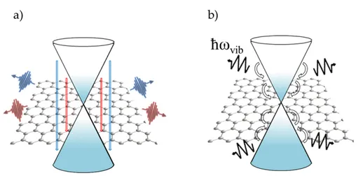
Figure 2.6: Sketch of the e-h pair recombination processes in graphene. a) Radiative channel: hot-luminescence; b) e-ph scattering on ps timescales (phonons with energy ~ωvib are depicted as zigzag arrows).
they create a highly nonequilibrium hot electron distribution, which first relaxes on an ultrafast timescale to a thermalized, but still hot, Fermi-Dirac distribution (Fig.2.5.b) and then slowly cools down eventually reaching thermal equilibrium with the lattice [76–87].
The entire scenario of experimental and theoretical studies points to the existence of two different timescales. A fast initial relaxation on a timescale of some tens of femtoseconds is responsable for the establishment of a hot Fermi Dirac distribution in the conduction band due to Coulomb- induced e-e scattering. This fast and efficient relaxation channel is associated to linear gapless dispersion band which guarantees the energy-momentum conservation required by the e-e scattering.
Once the hot Fermi-Dirac distribution is reached, the slower (hundreds of fem-toseconds) process is associated with carrier cooling and it can takes place through radiative mechanisms, known as hot-luminescence (Fig.2.6.a), and non-radiative mechanisms, such as e-ph scattering (Fig.2.5.b). Optical-phonons [78, 81] are the first (in time) relaxation channel of excited electronic states, due by the strong cou-pling of electrons with optical phonons near the K and Γ points in correspondence with Kohn anomalies. The e-ph scattering can be intra or interband and intra or intervalley. The intraband intravalley e-ph scattering involving an arbitrary small momentum transfer is the predominant mechanism. Indeed, interband scattering is
2.5. Ultrafast dynamics in graphene 21
Figure 2.7: Temporal evolution of the angle-integrated population, i.e. the occupa-tion of the conducoccupa-tion band times the density of states (DOS) after excitaoccupa-tion with laser pulse at t=0. (Adapted from [76]).
less efficient as, in order to relax to the valence band, all electrons have to cross the vicinity of the K point, which has a low density of states and therefore acts as a bottleneck for the dynamics. Moreover, inter-valley scattering processes involve two different Dirac cones. Therefore a large momentum transfer to scatter electrons be-tween two cones is needed, and the scaling of the Coulomb matrix with 1/q2 (where
q is the exchanged momentum) suppresses these processes. Consequently the inter-valley scattering plays a minor role in the relaxation dynamic in graphene. Moreover, acoustic phonons are essentially decoupled with the electronic states but they are coupled with the optical phonons acting on a timescale longer than a picosecond.
These relaxation mechanisms are shown in Fig.2.7, wherein the population of the conduction band integrated over the angle is calculated, looking at the dynamics shortly after an optical excitation at 1.6 eV and 10 fs f temporale duration [76]. Before the pulse arrives, a slight Fermi tail reaches into the conduction band due to the finite temperature. The laser pulse creates a non-thermal population 800 meV above the band crossing. After 10 fs, the distribution has already partly relaxed and the distribution function 30 and 40 fs shows only minor differences. This is due to the finite population of the initially quasi-unoccupied phonon modes.
The ultrafast dynamics of the electronic distribution has been object of several works both experimental [66, 78, 86, 88] and theoretical [76, 77, 79–85, 87] for the
pur-2.5. Ultrafast dynamics in graphene 22
pose of determining the temporal timescale and the parameters that affect it. In particular, monitoring graphene transient absorption [86] enables the direct mea-surement of the distribution function in real time. For example, the time-evolving hot-electron distribution inhibits, due to Pauli blocking, the absorption of the probe pulse at lower photon energies with respect to the pump, thus yielding an increase in transmission. Furthermore, the time evolution of these transient measurements gives access to the typical timescales characterizing the electrons dynamics [66, 78, 86].
Generally when a system is photoexcited, the relaxation towards equilibrium condition involves also radiative processes. In particular, among the single-photon interaction, fluorescence corresponds to the emission of redshifted light. Indeed, in semiconductors systems the e-h pairs, generated by the light-matter interaction, firstly relax on the bottom of the conduction band through intraband phonon-induced scattering. Then, the pair recombinate, emitteing light. The absence of a gap in graphene prevents any emission of light. Indeed, the fast e-e and e-ph scattering act on timescale much shorter than those of the typical recombination, without emitting photons [3].
Nevertheless, graphene could emit light if the fast non-radiative channels were slowed down [61, 63, 64, 89, 90]. For example, photoluminescence emission from graphene is observed after impulsive photoexcitation. Indeed, the high peak power promotes a large electronic density in the conduction band. This clogging effect prevents the action of e-e and e-ph decay channels, facilitating the radiative one. This emission is observed in both Stokes and Antistokes side and shows a non-linear dependence on fluence. The blueshifted emission at increased fluence and nonlinearity allows to preclude the conventional hot-luminescence, while the large non-quadratic variation of the emitted light as a function of fluence excludes the possibility to address it to two-photon absorption. The graphene nonlinear PL is particularly efficient and broadband due to several unique properties of graphene: i) carrier-carrier scattering requires both energy and momentum conservations, which are readily satisfied in the linear bands of graphene; ii) the line bands lead to a sym-metric distribution of non-nequilibrium electrons and holes, which facilitates direct recombination of excited e-h pairs; iii) the energy acquired by an e-h pair via
intra-2.6. Raman Spectroscopy 23
band scattering cannot be more than its kinetic energy, which equals~ω − Eg, and
it is the maximum in gapless materials such as graphene; iv) The greatly reduced dielectric screening in the 2D graphene results in a very high Coulomb scattering rate that is essential for establishing the strong e-h recombination [91].
This non equilibrium photoluminescence recalls the grey body emission and can be in first approximation described by Planck’s law [61, 62, 64, 67]:
I(~ω, Te) = R(~ω)τemη ~ω 3 2π2c2 ( ekTe~ω − 1 )−1 (2.5.14) where η is the emissivity, defined as the dimensionless ratio of the thermal radiation of the material to the radiation from an ideal black surface at the same temperature as given by the Stefan-Boltzmann law [92], τem is the emission time and R(~ω) is
the frequency-dependent, dimensionless responsivity of the detection chain. Refs. [61, 62, 67] reported that, although Eq.2.5.14 does not perfectly reproduce the entire grey body emission, the good agreement on a∼ 0.5eV energy window is sufficient to extract Te. Furthermore, hot-luminescence emission is a notable fingerprint of the
out-of-equilibrium electronic distribution.
2.6
Raman Spectroscopy
Raman spectroscopy [93] is based on the inelastic scattering of an incoming electro-magnetic field (νo), that produces a change in the polarization of sample’s molecules.
When a system interacts with an intense electromagnetic source, most of the light is scattered by the sample without changing its wavelength through an elastic pro-cess, called Rayleigh Scattering. Nevertheless, the coupling between the vibrational modes (νvib) of the sample and the driving frequency of the electric field is able to
generate new spectral components (see Fig. 2.8). The system changes its vibra-tional state following the incoming photon and it can reach a virtual excited state. Subsequently, it will spontaneously relax back to ground state: this explains the strong Rayleigh component in the spectrum. If the system relaxes back to an ex-cited vibrational state, the emission of Stokes (redshited) photons: νs = νo − νvib
is observed. Moreover, it is necessary to consider the possibility that the Raman process can be activated from an excited vibrational level: relaxation to the ground
2.6. Raman Spectroscopy 24
state will generate the emission of light at higher frequency, named the Anti-Stokes (blueshifted) component: νas = νo+ νvib. The inelastic scattering of light is known
as the Raman effect, named in honor of Indian scientist Sir Chandrasekhara Venkata Raman (1988-1970), who discovered this effect in 1927 [93].
Remarkably, only a tiny fraction of the scattered light (typically one photon over ten millions) is scattered inelastically, which justifies the spread of this spec-troscopic technique after the invention of the laser. Due to a small cross section (∼ 10−30cm2/molecule), spontaneous Raman has a very weak signal and requires
high laser power and long integration times. In addition, the signal is often over-whelmed by a fluorescent background from the sample, limiting its application. In a real experiment we do not probe a single molecule, but an assembly of molecules with their random initial phases and orientations; thus each of them will act as an independent source of radiation, that will sum incoherently, spreading in a 4π steradian solid angle. Although we can collect only a small fraction of the produced signal, Raman spectroscopy overcomes the limitations of IR spectroscopy [94]. Un-like Raman scattering, infrared spectroscopy is based on changes of dipole moment and, for centrosymmetric molecules, IR and Raman spectroscopy are completely complementary. Although infrared spectroscopy is also a powerful tool in imaging, it is limited to low spatial resolution because of the long wavelength of light used. Furthermore, the absorption of water in the infrared region makes it difficult to use for samples rich in water. However this absorption does not limit the applicability of Raman spectroscopy, thanks to a wider range of tunability for electromagnetic sources used. After all, in Raman process a single intense narrowband laser is able to provide information about all possible vibrations of a sample, whereas for IR ab-sorption a narrowband laser would give access to a limited narrowband abab-sorption. Nowadays, Raman spectroscopy is widely used characterization tool for studying liquids, gases and solids [95, 96].
2.6.1
Classical picture of light scattering
In the classical framework, the incoming electromagnetic field Eo induces
2.6. Raman Spectroscopy 25
Figure 2.8: Output frequencies of spontaneous Raman process.
of the crystal:
µ(t) =−er(t) (2.6.15)
where r(t) quantifies the motion respect to the equilibrium position and it depends on the interaction between the charge and the nucleus. Moreover, we define the macroscopic polarization P(t):
P(t) = N µ(t) (2.6.16) In the linear response limit - i.e.low intensity field and harmonic binding potential energy - P(t) is related to Eo by:
P(t) = ϵ0χ(1)E0(t) (2.6.17)
where ϵ0 = 8.85· 10−12F · m−1 is the electric permittivity in the vacuum and χ(1)
is the first-order electric susceptibility and represents the efficacy to perturb all the electronic charge density out of their equilibrium condition. Generally, χ(1) is a
second rank tensor but, without loss of generality, we assume that the crystal is isotropic so that χ(1) is represented by a scalar. The driving frequency of a visible
electromagnetic field is in the THz region, causing only the motion of the electronic density, i.e. the nucleus are too heavy to adiabatically follow the field and the electronic resonances are due to the electrons. Despite of it, the electronic density
2.6. Raman Spectroscopy 26
adiabatically adjusts to the nuclear motion to minimize the energy of the system. Hence, the induced dipole is related to E0 by the electronic polarizability α(t):
µ(t) = α(t)E0(t) (2.6.18)
As α(t) varies with the nuclear motion, it can be expanded as a Taylor series in the atomic displacement Q(t). At first order in Q(t), we have:
α(t) = α0+ ( ∂α ∂Q ) 0 Q(t) (2.6.19)
∂α/∂Q indicates how the polarizability α spatially changes in the molecule and
the subscript 0 stands for the equilibrium position of the atoms. A given atomic vibration can be decomposed into a sum of normal modes (i.e.phonons), therefore the nuclear motion can be approximated, without loss of generality, as a phonon of frequency ωv and wavevector k:
Q(t) = 2Q0cos(ωvt− k · r + ϕ) (2.6.20)
Substituting Eqs. 2.6.18 and 2.6.19 and 2.6.20 into Eq. 2.6.16 and assuming that the incident field E0(t) is monochromatic, E0(t) = Ae−i(2πν0t−ki·r)+ c.c., we have:
P(t) =N α0Acos(2πνot− ki· r)+ +N ( ∂α ∂Q ) 0 · QoA 2 (cos[2π(νo− νvib)t− (ki+ k)· r]+ +cos[2π(νo+ νvib)t− (ki− k) · r]) (2.6.21)
The linear polarization P, induced on the sample by electromagnetic field Eo, is
given by the sum of three terms, depicted in Fig. 2.8:
• The elastic component (Rayleigh scattering) oscillates with the same frequency νi of the incoming electric field and it has the same wavevector ki.
• The Antistokes term oscillates with a frequency νs = νi + νvib and has a
wavevector ks = ki + k. This component is blue-shifted and it is associated
to the annihilation of a phonon of frequency νvib and wavevector k.
• The Stokes term oscillates with a frequency νs = νi−νvib and has a wavevector
ks = ki− k. This component is red-shifted and it is associated to the creation
2.6. Raman Spectroscopy 27
Notably, a normal mode of the sample is Raman-active if the polarizability is changed during the vibration, i.e. ∂α/∂Q̸= 0 [97]; actually there must take place a change in the shape, dimension or orientation of the electronic distribution.
Otherwise, any Raman signatures are observed. In addition, Eq. 2.6.21 high-lights the two fundamental relations for Raman scattering: energy and momentum conservation.
νi = νs± νvib (2.6.22)
ki = ks± kvib (2.6.23)
The process just depicted corresponds to first-order Raman process because it involves only one-phonon. However, the description can be easily extended to higher orders in Q, rising to multiple-phonon Raman scattering. Remarkably, Eq. 2.6.23 shows another important properties of Raman scattering: one-phonon Raman scat-tering in crystals probes only zone-center phonons, i.e. phonons with q ∼ 0. How-ever, multiple-phonon processes can still probe others points of the first Brillouin zone but the total phonon wavevector must be equal to zero [98].
The intensity of the scattered radiation Is can be calculated from the
time-averaged power radiated by the induced polarizations P into unit solid angle. It will depend on the polarization of the scattered radiation es, es, as |P · es|2. We deduce
that Is is proportional to:
Is ∝ νs4|ei· ( ∂α ∂Q ) 0 Q0 · es|2 (2.6.24)
where ei is the polarization of the incident radiation. Notice that the scattered
intensity is proportional to the vibration amplitude Q squared. In other words, there will be no scattering if no atomic vibration is present. Moreover, Is depends on the
forth power of νs. Consequently, short wavelenghts are scattered more efficiently
than the longest ones.
We can now define a complex second rank tensor, the Raman tensor, as:
R = ( ∂α ∂Q ) 0 Q0 |Q0| (2.6.25) and the Raman intensity can be expressed as:
2.6. Raman Spectroscopy 28
Notably, the scattering radiation vanishes for certain choices on the incident and scattered polarizations. These so-called Raman selection rules are very useful for determining the symmetry of Raman-active phonons. The simplest example of Ra-man selection rules can be found in centrosymmetric crystals. In these crystals, phonons can be classified as having even or odd parity under inversion. Since the crystal is invariant under inversion, its tensor properties, such as (∂α/∂Q), should remain unchanged under the same operation. On the other hand, the phonon dis-placement vector Q of an odd- parity phonon changes sign under inversion, implying that (∂α/∂Q) changes sign. Hence the Raman tensor of odd-parity phonons in cen-trosymmetric crystals (within the approximation that the phonon wavevector is zero) must vanish [98].
2.6.2
The quantum description
Classical description of Raman scattering in condensed matter is similar to that in molecules, but it refers to the atomic vibrations in terms of phonons. Nevertheless, the main differences, occuring when substituting a discrete level system with an energy band one, could be enlightened by introducing microscopic quantum the-ory. To describe microscopically the inelastic scattering of light by phonons in a semiconductor, we have to specify the state of the three systems involved: incident and scattered photons with frequencies ωi and ωs, respectively; the electrons in the
semiconductor and the phonons involved in the scattering. The scattering proceeds in three steps [98, 99]:
• The incident photon excites the semiconductor from an initial state |i⟩ into an
intermediate state |a⟩ by creating an electron-hole pair (or exciton), via the electron-radiation interaction Hamiltonian, HeR.
• This electron-hole pair is scattered into another intermidiate state |b⟩ (e-h
pair) by emitting (Stokes) or annihiliting (Antistokes) a phonon of frequency
ωvib via the electron-phonon interaction Hamiltonian (EPC), HEP C.
• The electron-hole pair in |b⟩ recombines radiatively with emission of the
2.6. Raman Spectroscopy 29
Figure 2.9: Feynman diagram of the Raman Stokes process described in the main text. The incident (ωi) and scattered (ωs) light are represented with green and
red dashed arrows. The emitted phonon has a frequency ω0 and it corresponds to
the blue dashed arrow. |a⟩ and |b⟩ are the two electronic intermediate states. The vertex corresponds to the quasiparticles interaction: the Hamiltonian involved in each vertex is indicated.
The intermediate states |a⟩, |b⟩ can be either real states (i.e. they correspond to eigenstates of the system) or virtual states (i.e. they do not coincide with any eigenstates of the system). Notably, virtual transitions do not have to conserve energy, although they still have to conserve momentum. If at least one of these two states is real, the process is said to be resonant.
Feynman Diagrams
As long as all the interactions in the above Raman scattering processes are weak, the scattering probability (for phonons) can be calculated with third-order perturbation theory [99]. However, it is not a trivial matter to enumerate all the terms involved in such a third-order perturbation calculation. This is usually done, systematically, with the help of Feynman diagrams. The rules for drawing Feynman diagrams are [98, 99]:
• Excitations such as photon, phonons and electron-hole pairs in Raman
scat-tering are represented by lines (or propagators).
• The intersection between two propagators represents the interaction between
2.6. Raman Spectroscopy 30
• The annihilation or creation of a quasiparticle in the interaction is indicated
by the excitation propagator with an arrow. When the arrow points towards a vertex, the excitation is annihilated. Otherwise, it is created.
• Once a diagram has been drawn for a certain process, other possible processes
are derived by permuting the time order in which the vertices occur in this diagram.
An example of Feynman diagram of the Raman Stokes process is shown in Fig.2.9. The probability to scatter a system from the initial state |i⟩ can be derived, via the Fermi Golden Rule [98, 99]. In the case depicted in Fig.2.9, we have:
Is∝ |a>,|b>∑ < i[|H~ωeRi− (E(ωs)|b >< b|Ha− Ei)][~ωEP Ci− ~ω|a >< a|H0 − (EbeR− E(ωii))]|i > 2 × δ[~ωi− ~ω0− ~ωs] (2.6.27) where Ei , Ea and Eb are the energy of the states |i⟩, |a⟩ and |b⟩, respectively. The δ-function indicates the energy conservation condition. Note that the summation
on all the possible intermediate states|a⟩ and |b⟩ has to be taken into account. To have the complete response, it is necessary to consider all the six terms of the series, calculated in Ref. [98, 99].
Stokes and Antistokes intensites ratio
Classically, the probability of Stokes and Antistokes processes is the same. On the contrary, the quantum theory shows that the probability to annihilate or create a phonon depends on the phonon statistics, which is given by the Bose-Einstein distribution function [98–100]. At a given temperature T , the average number of phonons nvib(T ) with energy Evib is given by:
nvib(T ) = 1 exp ( Evib kBT ) − 1 (2.6.28)
where kB = 1.38·10−23J K−1the Boltzmann constant. The probability for the Stokes
and Antistokes processes differs because in the Stokes process the system goes from
nvib phonons to nvib+ 1, while in the Antistokes process the opposite occurs. Using
2.7. Raman spectroscopy in graphene 31
(Stokes) and from nvib+ 1 to nvib (Antistokes) are the same, and the intensity ratio
between the Stokes (Is) and Antistokes (Ias) signals are: Is Ias ∼ ωs4 ω4 as exp ( Evib kBT ) ∝ nvib + 1 nvib (2.6.29)
Note that the impact of the ratio ω4s
ω4
as is typically much smaller thanthe exponential
thus Ias is expected to be less intense than Is, a condition which is ubiquitously
observed in most material systems. Moreover, Raman spectrum can be used as a thermometer for the sample, just by considering the ratio Is
Ias, which depends
univocally on T . Indeed, for T → ∞ the ratio is equal to 1 and the two intensities are equal, as in the classical case. It is important to remember that the time reversal assumption does not hold when resonance Raman scattering with sharp energy levels takes place. In this case, strong deviations from Equation 2.6.29 can be observed [101–103].
2.7
Raman spectroscopy in graphene
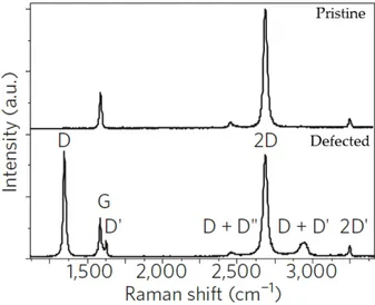
Figure 2.10: SLG Raman spectra in pristine (top panel) and defected (bottom panel) case. (Adapted from Ref [12]).
The first researches about Raman processes in solids can be dated back to 1960s [104,105], but graphene differs from usual semiconductors in several aspects. First of
2.7. Raman spectroscopy in graphene 32
Figure 2.11: Examples of Dirac cone formalism applied to three Raman processes responsable for G (a), D (b) and 2D (c) modes.
all, the linear gapless electronic dispersion implies resonances for any laser frequency
ωi. Secondly, excitons cannot be intermediate states due to the gapless energy
dispersion. Third, in the IR-visible range the electronic spectrum has approximately symmetric conduction and valence bands, while in semiconductors we can often consider the following inequality mh ≫ mefor effective mass m of holes and electrons
[12].
The first Raman spectrum of graphite was measured in 1970 [106], but the full theoretical understanding of this spectrum was only achieved in the years 2000-2010 [39]. In 2006 [107] the first Raman spectrum of isolated monolayer graphene was performed. The SLG Raman spectra, shown in Fig.2.10, appears extremely simple: just a couple of very intense bands in the 1000− 3000 cm−1 region and few other overtones. Nevertheless, their shape, intensity and position allows us to deeply characterize our sample (e.g. number of layers, presence of defects, fermi energy), becoming a powerful probe in analysing both vibrational and electronic properties [12].
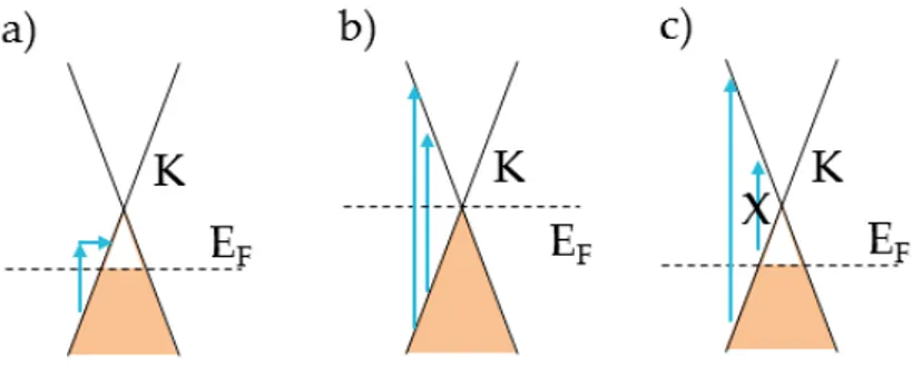
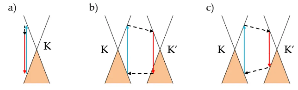
Dirac cone formalism [12] is a powerful understanding tool able to reproduce the main effects on the Raman spectrum. This graphical description, shown in Fig. 2.11, is set in the energy (y-axis) - momentum (x-axis) space. Solid black lines represent SLG electronic dispersion, i.e. the Dirac cones at K and K’ vertices. Band population is associated to occupied states (shaded areas). Interband transition are accompanied by photon absorption (blue arrows) and emission (red arrows). Phonon emission corresponds to intraband transitions (dashed arrows). Defect activated
2.7. Raman spectroscopy in graphene 33
Figure 2.12: a) Frequency of G mode vs number of stacked layers. The inset shows the G peak for HOPG (upper peak), double- (middle peak), and single-layer (lower peak) graphene. The vertical dashed line indicates the reference value for bulk graphite. (Adapted from Ref. [108]). b) POS(G) and FWHM(G) at room temper-ature as a function of electron concentration and EF. Red squares and blue circles
indicated the experimental data, while blue and red line derives from the calculation. (Adapted from Ref. [109]).
processes imply the electron scattering on a defect, formalized as a phonon with zero energy (horizontal dotted arrows).
In the following we will briefly describe the main features of graphene Raman spectrum and explain the principal mechanisms that contribute to it.
One-phonon process: G-band
The G peak [110] is due to the in-plane bond stretching of sp2 atoms in graphene layer and it is attributed to E2g point symmetry, corresponding to Γ vertice in the
first Brillouin zone. It is the only one-phonon mode in the 1000− 3000 cm−1 region, that satisfies the correct symmetry and wavevector conservation, as q ∼ 0. This phonon is deeply correlated to the number of layers n; indeed the G-band intensity decreases with n (see Fig.2.12.a), while different researches shows that its peak position, which is about 1580 cm−1 in graphite, depends on n, observing a redshift