POLITECNICO DI MILANO
School of Industrial and Information Engineering
Master degree in Materials Engineering and Nanotechnologies
Department of Chemistry, Materials and Chemical Engineering “Giulio Natta”
Au-Sn Electrodeposition for MEMS oriented Wafer Eutectic Bonding
Supervisor:
Prof. Luca Magagnin
Co-Supervisor:
Dr. Mattia Pallaro
Thesis by:
Matteo Pace
ID 863564
Summary
List of tables ... 3 List of Images ... 4 List of Plots... 8 Abstract: ... 9 Riassunto ...101: Motivation and thesis organisation ...11
2: Background ...13
2.1: Electrodeposition ...13
2.2: Sn-Au ...23
2.3: Bonding ...33
3: Experimental ...45
3.1: Deposition and characterization...45
3.2: Electrolyte change and optimization...62
3.3: Bonding ...74
4: Conclusions and future outlook ...81
5: Characterisation techniques ...82
5.1 X-Ray Diffraction ...82
5.2 X-Ray Fluorescence ...83
5.3 Scanning Electron Microscopy...84
5.4 Energy Dispersive X-Ray Spectroscopy ...86
5.5 Profilometer ...86
5.6 Optical microscopy...87
Acknowledgements ...88
List of tables
Table 1: Deposited Tin parameters overview ...18
Table 2: (Y. Nakamura, 1994)...21
Table 3: Hardness evaluation table ...26
Table 4: intermetallic phases evolution ...30
Table 5: Bonding parameters...34
Table 6: Parameters for deposition characterization ...47
Table 7: Deposition rate caracterization parameters ...65
Table 8: recorded data for samples to be used in bonding process ...76
List of Images
Image 1: microscopy images of Sn deposits obtained through reverse pulse plating ...16
Image 2: Dependence of Hardness on Frequency ...17
Image 3: Dependence of Hardness on anodic current ratio ...17
Image 4: SEM micrographs showing the morphology of deposits plated with different current densities (a) 0,0833 A/cm2 (b) 0,1 A/cm2 (c) 0,2 A/cm2 (d) 0,3 A/cm2 (e) 0,5 A/cm2 (f) 1,0 A/cm2 (g) 2,0 A/cm2 ...19
Image 5: pH effect on surface morphology ...20
Image 6: Cyclic voltammetry for Sn deposition on Cu ...22
Image 7: Cyclic voltammetry for Sn deposition on Cu at varying sweep rates ...22
Image 8: Au-Sn phase diagram ...24
Image 9: Au-Sn phase diagram highlight...25
Image 10: Linear thermal expansion Vs. temperature °C ...27
Image 11: backscattered electron imaging of different Sn phases ...28
Image 12: Linear thermal expansion graphs for different intermetallic phases ...29
Image 13: XRD peaks...31
Image 14: XRD peaks...31
Image 15: SEM section phase analysis...31
Image 16: Temperature Vs. Time evolution graph in bonding process ...35
Image 17: Bonded section example schematic...37
Image 18: SEM section phase study of bonded wafers ...37
Image 19: Evolution over time of phases in SEM view in bonded section...38
Image 20: Phase evolution in bonded section while aging at 200 °C ...39
Image 22: White light and infrared analysis for effective sealing...41
Image 23: Step by step growth and etching to achieve points or lines of bonding material to be pressed on an equally printed opposite face, achieving bonding and hermeticity (Nanochip, 2009). ...43
Image 24: End result of a bonded set of microchips being currently produced by IEEE with a similar method and different starting components ...43
Image 25: Example of border seals, printed in the chosen metal composition to achieve sealing through bonding (IEEE). ...44
Image 26: Graphical representation of testing patterns ...48
Image 27: Graphical representation of experimental conditions ...50
Image 28: Profilometry test, 500 p/mm over 4mm, shows a steep step of 1,8µm and considerable irregularity ...51
Image 29: Profilometry test, 500 p/mm over 4mm, shows a step of over 1µm ...52
Image 30: Profilometry test, 500 p/mm over 4mm, shows expected roughness over the majority of the surface, but exhibits what may be interpreted as a spike ...52
Image 31: profilometry test, 1400 p/mm over 3mm, reasonable roughness, unexpected step ...53
Image 32: Profilometry test, 1400 p/mm over 3mm, reasonable roughness, perplexing sudden variation in surface morphology ...53
Image 33: SEM surface morphology 10kX magnification...54
Image 34: SEM surface morphology 25kX magnification...54
Image 35: Photograph of laboratory samples ...55
Image 36: Photograph of resin encased samples for section SEM testing ...55
Image 37: Group 32 SEM section view ...57
Image 38: Group 32 atomic percentage composition overlay ...57
Image 39: Group 33 SEM section view ...58
Image 40: Group 33 atomic percentage composition overlay ...58
Image 42: Test sample B3 SEM section, red line represents Au, green line Sn ...59
Image 43: Group 36 detected peaks, showing Tin Sulphate ...60
Image 44: Group 25 detected peaks...61
Image 45: Sample I, Group 59, surface morphology by SEM, magnification 10kX ...68
Image 46: Sample I, Group 59, surface morphology by SEM, magnification 30kX ...69
Image 47: Sample III...69
Image 48: Sample III Spectra for sectors identified in Image 47 ...70
Image 49: Sample II ...70
Image 50: Sample II Spectra for sectors identified in Image 49 ...71
Image 51: Magnification of Sample II ...71
Image 52: Photograpfh of whole Au-plated wafer before processing ...72
Image 53: SEM surface images of new "standard" deposits ...73
Image 54: XRD identified peaks for Group 64 ...73
Image 55: Graphical representation of experimental setup ...74
Image 56: SEM section analysis of groups 74 and 75 after bonding. Au atomic % presence represented in red, Sn represented in light blue ...76
Image 57: Group 75 SEM section after bonding and composition analysis of shown sectors ...77
Image 58:Group 76 SEM section after bonding ...77
Image 59:Group 76 SEM section after bonding and composition analysis of shown sectors...78
Image 60: Group 79 SEM section after bonding and composition analysis of shown sectors ...78
Image 61:Group 81 SEM section after bonding ...79
Image 62:Group 81 SEM section highlight after bonding and composition analysis of shown sectors ...79
Image 63:Group 82 SEM section after bonding and composition analysis of shown sectors...80
Image 65: Philips® X-pert PW1830® powder diffractometer ...83
Image 66: Fischerscope® X-Ray XDV®-SDD...84
Image 67: EVO50 SEM...85
Image 68: Microfocus model Laser UBM ...86
List of Plots
Plot 1: Effect of agitation on deposition rate ...49
Plot 2: Study of the effect of temperature on deposition...50
Plot 3: Day 0 Cyclic Voltammetry at different scan rates...63
Plot 4: Day 6 Cyclic Voltammetry at different scan rates...63
Plot 5: Day 10 Cyclic Voltammetry at different scan rates...64
Plot 6: Cyclic Voltammetry comparison ...64
Plot 7: representation of data from Table 7 ...66
Plot 8: Standard deviation trend over increasing deposition time ...66
Plot 9: Growth of the depositing Sn layer over time ...67
Abstract:
The scope of this study focusses on the parametrization and execution of an effective Au -Sn eutectic bonding process between wafers for the application in industrial MEMS hermetic sealing.
A thorough study of the materials and intermediate process steps is performed and detailed, exposing our starting points from both a known literature and intellectual standpoint.
Our first step concerned the deposition of Sn on industrial Au plated substrates of varying thickness.
This was faced with an approach aimed to reliable reproducibility by exploring the effects produced by the variation of key parameters and the subsequent establishment of a “standard” empirical deposition procedure to be employed in following tests
Issues encountered and solved brought us to better understand the stability properties of the electrolytes used and advisable preservation precautions for the same.
Through extensive Cyclic Voltammetry, XRD, SEM, XRF and optic characterization our de position process was standardized after having achieved a result deemed promising to be used in the bonding process.
Bonding was then performed following literature and empirically viable guidelines
A method to test the feasibility of the process proper and its dependence on temperature, pressure and treatment time was employed, substituting the traditional repeated analysis of the same sample over time with the simultaneous testing of samples produced under varying conditions.
This allowed us both to find the optimal bonding conditions and process parameters to achieve literature ideal final composition and to observe intermediate points in the reactions by employing parameters which promoted a slower kinetic evolution of the system.
The end result demonstrated the process feasibility under laboratory conditions, recording process parameters with output fitting theoretical literature understanding of the phenomenon.
Riassunto
Lo scopo che questo studio si prefigge è di ottenere un insieme di parametri utili ed affidabili per l'ottenimento di uno strato di bonding tra wafer tramite l'utilizzo del punto eutettico del diagramma intermetallico oro-stagno.
L'intento applicativo di questa ricerca trova utilizzo nel campo della microelettronica in cui la chiu sura ermetica dei circuiti integrati e le loro capacità di gestire il calore sono, di anno in anno, sfide sempre più ardue.
l'approccio intellettuale parte dalla necessità assoluta di affidabilità e ripetibilità, scopo primo e ultimo dell'intero studio.
Nelle pagine successive è raccolta un'approfondita ricerca bibliografica sui temi affrontati, utile premessa per noi in sede di pianificazione ed attuazione del lavoro stesso e per il lettore per inquadrare il processo mentale che ci ha condotto ad attuare varie scelte specifiche.
La suddivisione dello stato dell'arte della conoscenza scientifica attualmente disponibile è tripartita: ad un'introduzione al concetto di elettrodeposizione, con il suo studio nel caso specifico della deposizione di stagno su un metallo nobile, segue lo studio del diagramma di fase dei due metalli in esame, per poi concludere con la teoria del bonding vero e proprio.
Lo scopo ultimo di questa teoria è stato di inquadrare le nostre scelte, da una definizione dei parametri operativi delle varie fasi, alle interazioni dei componenti e materiali, fino a quantificare dei parametri ideali per poter definire un risultato come ideale o accettabile.
A corollario è incluso un capitolo con delle brevi introduzioni ai metodi e gli strumenti di caratterizzazione utilizzati.
A concludere, dopo la teoria e la pratica, seguono le nostre conclusioni e prospettive future per questo ambito di ricerca, un capitolo sui metodi di misura sperimentale ed il loro funzionamento ed infine doverosi ringraziamenti a chi ha contribuito a rendere possibile questo lavoro, in modo diretto, o in modo più ampio come fonti bibliografiche.
1: Motivation and thesis organisation
In the modern age, micro-electronic systems control and regulate most aspects of industrial, professional and personal lives.
Such a technology, permeating most levels of our society, is naturally driven by necessity to always improve in efficiency and affordability, ever challenging Moor’s Law for the miniaturization of the integrated circuit.
This ever growing need requires the implementation of cutting-edge technologies to achieve size reduction while accounting for one of the most arduous challenges for micro-electronics: heat management.
To face this problem, our study explores the suitability of an eutectic bond between gold and tin to be used as an hermetic sealant for MEMS due to its formidable properties apt to face the aforementioned
challenges.
Our work is divided in two main sections, chapter 2 and chapter 3, each internally subdivided in multiple parts, preceded by the proper introductions and followed by our conclusions after performing the study and future outlooks on the topic.
Finally, a section is reserved for a comprehensive recap of the testing methods used in the stud y and an appendix including all the experimental data from instruments that was not included explicitly in the written elaborate.
Chapter 2 defines bibliographical knowledge of the main areas required to understand and perform the experimental part of the study:
2.1 Electrodeposition: This first section defines our starting point on electrodeposition, exploring the process itself before focussing on the deposition of Sn on a noble metal substrate.
Here we explore various deposition techniques and approaches, both from a methodology and starting components standpoint, finally settling for the method used in following practical sections with understanding of both positive and negative aspects in accordance with laboratory availability. 2.2 Au-Sn: In this kind of study, an in-depth understanding of the metallurgical properties of the materials in use is paramount.
This section starts from a comprehensive study of the multiphase diagram of Au and Sn, detailing all phases of interest, their properties, their interactions and their evolution in the eutectic formation.
Ultimately this led us to set an objective for our practical work, as it outlined the ideally desirable final composition and morphology of our bonding layer.
2.3 Eutectic bonding: Lastly, in order of logic and not importance, the background for the bonding process itself is laid with the state of the art knowledge readily available in literature, giving us the boundary conditions to operate within, to be optimized for our specific case.
Chapter 3 encloses the experimental part of our work, including and detailing procedures and the lines of thought that brought about certain procedural decisions.
3.1 Deposition and characterization: as the title implies, in this section we aimed to achieve a “standard” deposition procedure for the following work, varying temperature, currents and agitation in order to optimize the end result.
Already quite some data had already been gained as we encountered an issue in the outcome, leading us to an in-depth search for the cause, opening to the work done in the following paragraphs.
3.2 Electrolyte change and optimization: once the issue with the process had been identified, it was solved by changing both the electrolyte for a more stable solution and the substrate with a wafer plated in a thicker layer of Au (from 1 μm to 3 μm). Characterizations of the new components and the samples produced under newly established conditions brought to an understanding of the deterioration over time of the electrolyte and a new set of standard conditions for controlled deposition of Sn, enabling us to proceed once the results turned out to be satisfactory.
3.3 Bonding: In this final experimental paragraph we outline our findings in the bonding procedure, referencing our knowledge from previous chapters to determine that our results were, in fact, satisfactory for the intended objective, with an overview of the effect of various parameter changes.
In chapter 4 we then outline what could be considered to be the natural follow -up to this study, what challenges we faced and how to improve upon the work done, what we achieved ad what complementary tests could be perform to deepen the knowledge of the topic.
Chapter 5 includes an outlook on the characterisation techniques used and their worki ng principles.
2: Background
2.1: ElectrodepositionKeeping in mind the aim of this study, the process chosen to obtain a layer of Sn on Au substrate has been electrodeposition.
In order to obtain a compact and hard layer of metal, with good adhesion with the substrate while
controlling the width of the deposit, literature clearly outlines this method as the most straightforward [1].
As a process, electrodeposition is defined as the electrochemical reaction through which a metal coating is deposited on a conductive material (often another metal), by the external application of potential to what is called an “electrolytic cell” system through reduction-oxidation (Red-Ox) coupled reaction [2].
The reaction taking place at the cathode is as follows:
Mn+(aq) + ne- M(s) with the necessary electrons provided by an external power source.
The reaction leads to the formation of what is defined as a coherent metal coating under the driving force of the applied overpotential (η) , which shifts the electrodes potential from the equilibrium value at open circuit.
η = |Eref – Eref(OCV)|
In our endeavour we have been using as electrolyte a patented aqueous acid tin methanesulponate solution and both inert (Platinum plated) and sacrificial (pure Sn) anodes.
The efficiency of our reactions will be measured through the Faraday eq.
𝑚 = (𝑄 𝐹) (
𝑀 𝑧)
Where:
“m” is the mass of substance deposited at an electrode in grams
“Q” is the total electric charge passed through the substance in Coulombs
“F” is the Faraday constant 96485 C mol-1
“M” is the molar mass of the substance in grams per mol
“z” is the valence number of ions in the substance
Morphology and reaction rate may also be strongly affected by applied overpotential and/or concentration gradients in the solution (diffusion limiting current).
In the following pages, particular attention will be given to the present stages of knowledge regarding the electrolyte bath, its stability, obtained deposit hardness and morphology, taken as the starting points of the experimental phase.
Tin is known and widely used as an easily solderable material, with a melting point of 232 °C as p lated. Sn electrodeposition has a long history as can be found in detail in the book from M. Jordan
[3]
and can be performed from both acidic and alkaline baths.As for the knowledge involved in this process, even if it will not be directly employed in the following experiments, it would be remiss to not include mention of a deposition method using, instead of a continuous power, pulsed current to obtain deposition.
Mention of this technique for industrial use, aptly named pulsed electrodeposition, may be found in a patent [4] in which it is defined as “a process for electroplating tin and alloys thereof onto metal substrates using an aqueous plating solution”.
The process described involves the use of acid deposition electrolytes containing stannous alkoyl sulfonate combined with either alkyl sulfonic acid or alkoyl sulfonic acid in proportion such as to provide a solution with pH equal or lower than 1.
Working parameters require a concentration of stannous sulfate in the aqueous solution such to produce a metal concentration between 20 g/l and 110 g/l and between 100ml/l to 250ml/l of sulfonic acid
(considering the use of a 70% molar acid solution).
Moreover, the importance of additives is heavily stressed: “at least” one organic additive in reason comprised between 0,08g/l and 0,8g/l is required for ideal efficiency, showing at least one heterocyclic moiety and one aromatic moiety. Examples provided as heterocyclic are lactones, cyclic imides and oxazolines, while pheniles and phenols are suggested as aromatic groups.
Mention of Polyalkoxylated alkyl phenol is made as a suitable further additive to prevent dendritic growth on the deposition surface (between 0,5g/l and 4g/l).
While what just described is characteristic of a specific process, it is paramount to note the influence process parameters have on the end results of morphology and hardness of the deposit have been thoroughly studied, with a staple being the Osero study in 1986
[5]
.Following, a consideration of the present state of knowledge on the differences between deposition with acidic and alkaline electrolytes.
As noted in literature [6] alkaline baths are based on sodium and potassium stannate (Na2Sn(OH)6– K2Sn(OH)6).
This provides for these baths a simpler formulation, a wide range of operating concentrations yielding satisfactory deposits, no need for additives, wide impurity tolerance, are easily controlled and show excellent throwing power .
On the other hand, in alkaline electrolytes we find the thetravalent Sn form, stannate ions (SnO44-), having an electrochemical equivalent which is half than the respective active divalent ion in acid baths (stannous ion, Sn2+).
Moreover, the elevated operating temperatures make the plating on delicate substrates dif ficult, no bright deposits can be obtained under direct current deposition without using complex post treatments and the use of a soluble anode requires a critical control.
In the experiment performed by Hansal et. al. both a preliminary test in direct current and pulsed current were made.
The direct current testing was performed through Hull cells on steel sheets to ascertain operating currents.
A hull cell is a testing tool, or a miniature electroplating cell, in which an electroplating solution is evaluated across the range of operating conditions. An evaluation of the deposit on the cathode across a range of current densities is useful in demonstrating the capabilities of a plating bath solution.
It was noted that for current densities inferior to 200A/m2 a matt deposits obtained, while above this value porosity and dendritic formations begin to show, attributed to a competing hydrogen evolution reaction.
This effect, already tipical for high current densities in Hull cells, may be enhanced due to the tipi cal instability of reaction intermediates happening at the anode:
𝑆𝑛 + 4𝑂𝐻 + 4𝑒− → 𝑆𝑛(𝑂𝐻)42−
2𝑆𝑛(𝑂𝐻)42−→ 𝑆𝑛0+ 𝑆𝑛(𝑂𝐻)62−+ 2𝑂𝐻−
It i salso noted that a current too low may also lead to dendritic formation, with a mixed polycristalline growth
[7]
.Considered next is simple pulsed current, defined as a sequence where a cathodic current pulse is applied during a time interval (called “on”) followed by an “off” time at zero current periodically repeated.
General visual results remain consistent with direct current deposition, matt for low current densities, powdery deposit for higher currents than 500A/m2. The higher critical current for deposit morphology
change is to be attributed to the fact that in pulsed plating to obtain a consistent average current concentration in respect to direct current deposition, the pulsed current will have a higher intensity.
The off times to offset hydrogen evolution damaging effects must be properly considered.
To solve this aspect, a duty cycle of 10% was used, showing dramatically increased deposit properties, safe for extremely high current densities (circa 1000 A/m2).
Longer off times allow for the desorption of H2 bubbles from the cathode, leading to more unuform deposits. Moreover it is considered that the off time allows for the relaxation of the disequilibrium
concentration profile at the interface due to mass transport and for a partial relaxation of residual stresses potentially responsible for whisker formation.
Frequency does not appear to have major effects on the results.
A study on reverse pulsed plating, a process in which the cathodic pulse is alternated with an anodic current pulse, was made, showing that the range of cathodic to anodic current per sequence for operating conditions is limited to values between 9 and 4.
This process, while considerably harder to fine tune and industrially streamline, offers the possibility of a very stable deposit, due to the fact that the inverse current (anodic) pulse allows for a re -dissolution of impurities (dendrites) with higher reactivity and a balancing of the active species, leading however to deposit brittleness for low ratios.
Image 1: microscopy images of Sn deposits obtained through reverse pulse plating
Hardness is, in fact, a very important parameter, especially for a material such as tin that is very soft, which may lead to its inapplicability to electronic systems if minimum values are not guaranteed for the deposits.
Using literature knowledge [8] as a reference for optimal deposition conditions, micro hardness tests were performed showing that while a direct current deposit had a matt finish and relatively low hardness (16HV), pulse plated deposits were brighter, smoother and harder (27HV).
Hardness dependence on operating parameters was analysed more in depth for the reverse pulse plating processes, as follows, depending on frequency (Hz) and cathodic to anodic current ratio (Qc/Qa).
Image 2: Dependence of Hardness on Frequency
Image 3: Dependence of Hardness on anodic current ratio
Acid electrolyte pulsed plating
Acid baths are based on stannous sulphate or tetrafluoborate. The electrochemical equivalent is twice that from the alkaline baths. Furthermore, it is possible to obtain bright coatings by using organic additives; the baths are operating at room temperature and can be used for the plating of delicate substrates.
Nevertheless, especially due to the use of additives, a thorough control of the bath composition is important.
The main and most forthcoming issue in the electrodeposition of tin in acidic baths is its propensity to the formation of whiskers, reaching micrometres in length [9] .
This extremely undesirable formation is strongly influenced by surface morphology and microstructure parameters, such as film thickness, grain shape and size, applied stresses (external) and substrate.
Various parameters are explored:
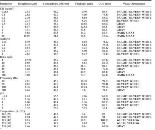
1. Current density: mainly affecting nucleation and deposition rate
a. 0,083 A/cm2<CD (current density)<0,3A/cm2: uniform and bright deposit, well developed equiaxial grains, coherently with the knowledge that nucleation rate increases with CD, resulting in smaller grains
b. 0,5 A/cm<CD<1 A/cm2: Current efficiency droppes due to diffusion of Sn2+ in the
electrolyte. Hydrogen evolution starts, dendritic formations appear instead of the previous uniaxial growths.
c. 2 A/cm2<CD<10.0 A/cm2: hydrogen evolution critical, porosity evident in the deposit.
Image 4: SEM micrographs showing the morphology of deposits plated with different current densities (a) 0,0833 A/cm2 (b) 0,1 A/cm2 (c) 0,2 A/cm2 (d) 0,3 A/cm2 (e) 0,5 A/cm2 (f) 1,0 A/cm2 (g) 2,0 A/cm2 (h) 5 A/cm2 (i) 10 A/cm2
2. Duty cycle: deposition rate in this technique is regulated by the Pulse Current density (Jc), on and off time, respectively (Ton, Toff). At a given Jc duty cycle Pct is given by
𝑃𝑐𝑡=
𝑇𝑜𝑛 𝑇𝑜𝑛+ 𝑇𝑜𝑓𝑓 Thus the average current Ja
𝐽𝑎= 𝑃𝑐𝑡× 𝐽𝑝
SEM micrographs with varying parameters show that grains tend to be finer as duty cycle and/or Ton increase. It is however reported that in both Sn and Zn deposits, over a duty cycle of 44 grains tend to grow, as if approaching a direct current deposition behaviour [10].
3. Effect of pH on surface morphology: as can be seen in (Image 5), for -0,1<pH<1, grain refinement is observed (a-b-c), leading to a more porous deposit (d) for pH higher than 2-3 (due to the onset of hydrogen evolution), leading to powdery deposits for pH>3.
Image 5: pH effect on surface morphology
The powder deposition may be attributed to phenomena of precipitation of stannic hydroxide following this eq:
𝑆𝑛2𝑂𝐻 + 𝑂𝐻 → 𝑆𝑛𝑂𝐻++ 𝑆𝑛𝑂𝐻𝑎𝑑𝑠+ 2𝑒−
Highest current efficiency was shown to be obtained for pH values comprised between -0,1 and 0,5. 4. Temperature effect:
Experimenting maintaining all parameters constant except for T, it was observed that temperature in fact affects the deposit morphology.
The observed trend gives smaller grains for room temperature, with dimensions increasing with temperature.
Tis is due to two concurring effects: a higher mobility of metal ions (leading to faster growth and lower overpotential), and an increase in the nucleation energy barrier ΔG according to the Glasstone equation related by Hempelmann [11].
∆𝐺 ∝ { 1 (𝜂 + [𝐶′𝐶]) 2 }
The current efficiency is maximum at 313 K (40 °C) , but then a slight drop is observed. It is reported in the literature that in acidic aqueous solutions, the solution may decompose at higher temperature resulting in a visible colour change from light to dark yellow [12].
While with acidic electrolytes the reacting ion is the stannous ion Sn2+, in alkaline ones we have usually tetravalent stannate ions SnO4
4-. Choice between using different types of electrolyte solution may depend on applicable parameters keeping in mind the end properties of the deposit, which are influenced by current density, electrolyte throwing power, cathode efficiency ecc.
For a process with such a rich history, many possible combinations of electrolytes and additives have been explored, as can be found in [table 1], however for this work the process we have decided to focus on has involved the recent studies of [13] on methanesulfonic acid electrolytes.
In the study deposition baths based on sulphuric acid, methanesulphonic acid and phenolsulpohnic acid have been compared, yielding interesting results.
While comparatively cheap, the sulphuric acid bath proved to act as an oxidant for stannous ions in solution, leading to precipitation and deposition agent depletion in the electrolyte. High current densities also proved to polarise the anode, limiting this bath to low speed depositions.
Phenolsulphonic based electrolytes have been discarded for the industrial purpose of this study not only for having lower conductivity, but mainly for being toxic, hazardous and a dangerous pollutant.
Methanesulphonic baths are more expensive, but are on the other hand organic, biodegradable and less corrosive, being overall more convenient. Moreover, it has be en noted that Sn deposition with this electrolyte favours surface finish and is improved while depositing on a nobler metal, such as copper, rendering it a favoured candidate for use in deposition on gold substrate.
Table 2: Specificata fonte non valida.
In our study, a methanesulphonate based electrolyte was used, following considerations.
As noted in literature [14] this particular bath is being explored and researched in recent years for mass industrial applications, mainly for its favourable metal solubility, low environmental impact and corrosivity, but mainly for its low oxidation rate, compared to other organic/biodegradable electrolytes.
Cyclic votammetry tests, described in depth in chapter 3.3, were performed with this bath for Sn deposits on Cu substrate (fig. a)
Forward scans, performed from 0 to -0,8V versus Ag/AgCl show a single reduction peak (A point) for tin, corresponding to a single two-electron transfer step
𝑆𝑛2++ 2𝑒−→ 𝑆𝑛
The deposition of metallic Sn began at 0,444V versus Ag/AgCl, with an OCV (open circuit voltage) of -0,429V vs. Ag/AgCl in static conditions.
As the electrode potential became more negative, the current density reached a maximum and then decreased to a plateau, followed by an increase in current density (jp). This peak is to be attributed to the complete consumption of the Sn2+ at electrode surface due to mass transport control. Further peaks at more negative poitentials are due to hydrogen evolution at the tin deposit following equation
2𝐻++ 2𝑒− → 𝐻 2
On reverse potential sweep, a single stripping peak was observed (B point, Image 6), underlying the two electron oxidation step of metallic Sn to the ion form Sn2+.
CVs at different sweep rates showed no unexpected changes (Image 7)
Image 6: Cyclic voltammetry for Sn deposition on Cu
2.2: Sn-Au
The chosen materials for this study present interesting and very promising properties when applied together as a bonding medium.
As a deep knowledge of these characteristics underlying our work is paramount in order to explore the various possible approaches for industrial application, this chapter will be dedicated to the interaction of the two chosen metals in specific conditions of interest for practical use.
Keeping in mind the application in Micro Electronic systems intended, a semiconductor package is a key element of the integrated system for purposes of heat dissipation, mechanical support and electrical connectivity.
Chips or dies must be bonded to the semiconductor package in a way that is optimized to satisfy these purposes. For this purpose, a variety of materials is in common employ, such as hard solders, soft solders, metal filled epoxies and glass.
Hard solders, category to which the eutectic of Au-Sn belongs, have been used in the last 30 years because of their competitive properties as compared to soft solders.
Hard solders present a comparatively high strength, no thermal fatigue effects as well as no outgassing, all critical factors to account for in MEMS engineering. [15]
Between the most commonly used eutectic hard solders (Au-Ge, Au-Si, Au-Sn), Au-Sn has the lowest melting point, recorded at 280 °C (second lowest being Au-Ge at 361 °C).
This property is of the utmost interest, as many heat treatment sensitive materials are used as semiconductors, such as GaAs, leading to a preference in applying the least temperature straining procedures, favouring our material choice for this study.
Moreover, this particular material choice is favoured because, even though it presents a rather large mismatch in thermal expansion coefficients with Si, proper adhesion has been widely demonstrated [16] [17].
The choice is not, however, without points that need to be clarified: reaching eutectic concentration is paramount, as the formation of other intermetallic phases, the presence of voids and/or oxidation, to which Sn is particularly prone, require us to study the critical points of the applicable industrial process.
The presence of voids, together with undesirable alloys different from the eutectic concentration may lead to improper surface wetting resulting in incomplete wetting a brittleness of the bond. [18] [19]
While oxidation can be dealt with proper storage and processing in O2 free environments, a proper
understanding of the phase diagram of the metallic couple is fundamental to proceed in the exploration of the feasibility of large scale applications of this bonding medium.
Image 9: Au-Sn phase diagram highlight
As we can see this binary system is very complex, presenting four stable intermetallic phases, two eutectic points and at least 3 peritectic points.
The uncertainty is given by the complexity of the material, which has been studied over the last century at length, with a first draft being presented as soon as 1905 [20], but with ample development even in more recent years, leading to the diagram shown, which still has some uncertainties especially in Au -rich areas.
Some properties of the known phases themselves still need further research to be determined with accuracy.
The solid solution at the left side of the diagram presents the same crystal structure of Au, f.c.c., as it is a substitutional solid solution of Sn in Au, where Sn substitutes 6.6% of Au atoms in the crystal structure.
This situation is possible due to the fact that the atomic radiuses of the atoms involved are very similar: Au (1,59Å) Sn (1,63Å), with a discrepancy of 2,5%, which is far from the theoretical limit of 15% to allow for this phenomenon.
As the concentration of the second metal increases (Sn) at T above 532C° a liquid solution of the Au
terminal solution appears, leading to a varying range of freezing temperature for the alloy as Sn pe rcentage increases.
While for pure Au the melting T is 1064,43C°, at Sn atomic percentage of 29% the melting point drops drastically to 280C°.
In this area we have peritectic point which may or may not allow for the presence of a stable Au10Sn phase, however this has not yet been cleared beyond doubt.
The phases of interest for our study and of whose existence there is reasonable consensus, are AuSn, AuSn2 and AuSn4; we will now proceed to better understand their properties at the present state of knowledg e [21].
AuSn presents a B8 structure homologous to NiAs
AuSn2’s structure is not clearly defined, but its translational group is orthorhombic primitive AuSn4 has a large unit cell with orthorhombic translational symmetry
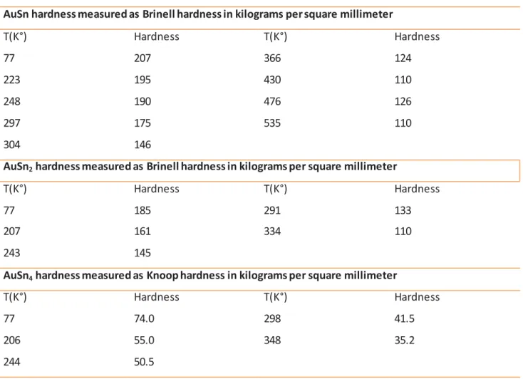
Hardness has also been evaluated for slices of quenched ingots of bulk material.
AuSn hardness measured as Brinell hardness in kilograms per square millimeter
T(K°) Hardness T(K°) Hardness 77 207 366 124 223 195 430 110 248 190 476 126 297 175 535 110 304 146
AuSn2 hardness measured as Brinell hardness in kilograms per square millimeter
T(K°) Hardness T(K°) Hardness
77 185 291 133
207 161 334 110
243 145
AuSn4 hardness measured as Knoop hardness in kilograms per square millimeter
T(K°) Hardness T(K°) Hardness
77 74.0 298 41.5
206 55.0 348 35.2
244 50.5
Apart from hardness, which is naturally a key element for a bonding medium, thermal properties must be taken into account due to the necessary heat treatments the part is subjected to during the industrial production process.
First and foremost, thermal expansion and subsequent elasticity problems must be reviewed.
As noted in literature [22] the usage of the specific 29 Sn atomic percentage eutectic has continued over many years showing little problems, but due to the complexity and uncertainties involved in the specific diagram in use, care is advised.
During preliminary studies in 1974 by Bernstein et. al. [15] an unusual dip in the thermal expansion coefficient vs temperature curve was observed and caused concern.
Image 10: Linear thermal expansion Vs. temperature °C
As established, such transition may indicate a change in physical properties due to a phase transition not previously detected. Such transition, especially considering that the alloy is used in hermetically sealed systems and takes place well within processing temperatures, may cause brittleness and/or loss of integrity due to considerable discrepancies in thermal behaviour.
Due to the great interest in the subject, contemporary studies were made, and in fact, as expected, metastable activity was discovered thanks to the work of Massalski [23].
The eutectic of interest is composed of two phases: a ζ phase, with approximate stoichiometry Au5Sn, and a δ phase AuSn, both shown in the diagram above.
It was discovered that approximately at 190C°, the ζ phase undergoes an order-disorder transition, defined as ζ ζ’, achieving a higher degree of crystalline order.
In Image 11, we find the backscattered electron imaging of different phases, in order left to right:
1. δ phase with ζ inclusions (lighter hue) 2. eutectic showing 46.6% δ phase (darker hue) 3. ζ phase, with 7,2% of δ phase
Image 11: backscattered electron imaging of different Sn phases
LTE (linear thermal expansion) (ΔL/L0) studies performed show in fact discrepancies in behaviour between the phases, especially regarding the eutectic.
The AuSn alloy showed an average CTE (coefficient of thermal expansion) of 14.0 ∙10-6/C° over process T range (23C°-250C°).
The eutectic shoved complexity: CTE of 16.2∙10-6/C° on heating to 16.8∙10-6/C° on cooling under transition T (190°). Above transition T, CTE was observed to vary, 15,6∙10-6/C° on cooling and 17.0∙10-6/C° on heating.
ζ phase showed similar behaviour to the eutectic, with a CTE of 17,8 ζ phase below transition temperature, becoming 21.2∙10-6/C° above transition temperature.
Moreover, eutectic and ζ phase showed a shrinkage of 0.34% over 4 subsequent days of annealing, as opposed to the much smaller 0.05% shrinkage over the same period of the AuSn phase.
Image 12: Linear thermal expansion graphs for different intermetallic phases
Electronic parts joined with this method usually have gold film on the mating faces which melts during the process, combining with Sn according to temperature and time, dete rmining the final composition overall.
This clearly leads to conclude that the actual bonding effects are produced by a combination of ζ phase and eutectic.
Even though using intermetallic metastable phases as a bonding medium seems unwise, due to their intrinsic risk of brittleness following thermal instability at room temperature (or any T<190C°), this alloy has been in use for over 3 decades due to its aptness under different operational aspects as already discussed.
This paragraph is not intended to dissuade from the use of AuSn alloys as bonding medium, but as a warning to account for the critical aspects of the material choice, greatly outweighed by the positive characteristics.
The ζ ζ’ transition is demonstrated to be a shrinkage transition and it must be stressed that in bonding and hermetic seals this must be considered in mechanical testing and requirements.
After accounting for possible reactions during processing and subsequent storage (as the shrinkage reaction elapses over only 5 days), ageing at room temperature has to be verified.
Careful study has in fact shown that the couple Sn-Au is extremely susceptible to diffusion, even at room temperature [24].
The first considerations in analysing literature about thin film interdiffusion between Au and Sn show that the most common phases to be expected are the Sn-rich ones, AuSn, AuSn2, AuSn4.
The absence for the other well-known phase in proximity of the desired eutectic concentration, the Au-rich Au5Sn is commonly attributed to the fact that diffusion of Sn in Au is kinetically hindered and very slow even at medium-high temperatures where it is commonly found, leading to the conclusion that room temperature diffusion will not show this phase in any detectable quantity in any reasonable time frame.
Studies on varying thickness of the relative metals right after depositions were performed [24] but we will focus on the Au/Sn couples, (Gold substrate, varying Sn deposit thickness).
Here we show the various compositions found through XRD patterning of various cross sections starting with different thickness of Tin deposit, over an increasing number of days.
In Table 4, phases are listed from most to less prevalent going from top to bottom, with a constant 1,5μm gold substrate on silicon wafer.
Image 13 shows the peaks obtained through XRD for the 0,25 μm Sn film for 0(a), 5(b), 10(c) and 30(d) days.
Image 14 follows the same descriptive pattern for a starting 1 μm Sn film.
Image 13: XRD peaks
Image 14: XRD peaks
It is clear that diffusion is not equally fast for the two metals: it is well known that group IB noble metals, such as gold, diffuse rapidly in IIIA and IVA host metals, such as Sn in this case.
Considering that gold diffusion at grain boundaries is expected to be even faster, that grain boundaries are expected in electrodeposited metal films to be abundant and that at room temperature the Sn diffusion substitutional mechanism is practically absent, we obtain an estimate 13-15 orders of magnitude difference in the diffusivity of Sn and Au, in favour of gold [25].
This, combined with the considerations of Gregersen et. al. [26], lead to the valid approximation of considering the gold mobile and Sn as immobile when coupled.
It was determined that Au migrates through AuSn even faster than it does through more Sn -rich phases AuSn2 and AuSn4. [26]
With this knowledge, we can start our work with the following expectations:
AuSn4 and AuSn phases are expected in all thickness deposits right after deposition.
In deposits where the Sn layer is less than 1/6 of the Au film thickness, only AuSn is expected to remain for any ageing time longer than 5 days.
For 1/3 Sn to Au layer thickness ratio the phases AuSn4, AuSn2 and AuSnare expected in reaction regions in this order.
For high thickness of Sn (2/1 ratio with Au), the same phase distribution is expected with pure Sn leftover.
AuSn and AuSn2 are continuous layers.
AuSn4 is a discontinuous layer, due to slight differences in the diffusion speed (grain size, orientation, grain borders).
At the AuSn/Au interface (or AuSn2/Au interface after ageing) Kirkendall voids are expected due to the fast diffusion of Au.
2.3: Bonding
Wafer bonding in micro and nano-dimensional electronic systems is defined as a packaging process able to ensure a mechanically stable and hermetically sealed encapsulation of the device.
Historically, this objective has been achieved in a variety of methods, from large scale soldering, to
complete resin encapsulation, but these processes have lost viability due to the ever decreasing size of the transistor and subsequently electrical components and systems in general.
As the need for a scaling down of dimensions became an ever growing challenge for the electronic industry as well as for the material sciences, the process verged towards a sealant in between two wafers, such as a glue, often silica or epoxy composites.
However, while the aforementioned materials do provide the mechanical requirements, as the scaling down doesn’t show a trend for stopping or slowing, thermal issues constituted the most pressing issue in the engineering of MEMS.
Thus, the most immediate choice was to opt for metals, whose properties seem to be best suited for the role:
Ductile and malleable lead to a reduced risk of brittle behaviour
High heat conductivity work as a highly efficient heat sink for the delicate circuits
In the liquid phase (or close enough to it), metals flow, especially if subjected to pressure, leading to a filling of eventual void, ensuring sealing
Reason for curiosity, metallic alloy options are extremely varied, allowing for a multitude of options to solve specific issues.
Eutectic alloys present various advantages regarding process temperatures, as already mentioned: in this chapter, we will focus on the specifics of the bonding process, its peculiarities and a detailed overview of the present knowledge of its use in wafer bonding.
Immediately casting aside the application of the eutectic alloy directly as a solder, which is impractical for the micro-scale due to deposition restrictions, we are going to talk about what is known “bonding layers” phenomenon.
By this we mean the achievement of the eutectic state in between opposing metallic faces of wafers after these are pressed together in suitable conditions of temperature, force and atmosphere.
While this allows for a minute control of the sites of bonding and the solder with through very precise deposition techniques of the original metal layers themselves, the problem of control arises.
Two are the driving phenomena leading layer bonding:
eutectic alloying: the metal layers achieve melting temperature and form the eutectic composition (less used), or an eutectic composition metallic layer is deposited on 2 opposing faces which are then fused together
atomic diffusion by thermo-compression bonding: bonding obtained by achieving eutectic composition at lower-than-melting temperature merely by the migration of a metal in the other, leading to adhesion.
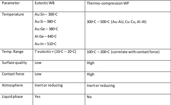
Various parameters can be immediately outlined for these processes:
Parameter Eutectic WB Thermo-compression WP
Temperature Au:Sn – 300◦C Au:Si – 380◦C Au:Ge – 380◦C Al:Ge – 440◦C Au:In – 510◦C
300◦C – 500◦C (Au-AU, Cu-Cu, Al-Al)
Temp. Range T eutectic + (10◦C – 20◦C) 100◦C – 200◦C (correlate with contact force)
Surface quality Low High
Contact force Low High
Atmosphere Inert or reducing Inert or reducing
Liquid phase Yes No
Table 5: Bonding parameters
In order to picture the temperature history of an ideal process, we add an example of thermal profile as given by [27].
Image 16: Temperature Vs. Time evolution graph in bonding process
What is observed, in literature as in following experiments, an ideal result is observed after a multi -step thermal treatment.
An initial heating is applied up to a T lower than the eutectic melting point, in order to preheat the samples uniformly.
Temperature is then increased steadily (in order to avoid heat induced cracks) slightly over the eutectic melting point: this allows for faster bonding kinetics.
Lastly we see the return at room temperature. Atmosphere in this process must be con trolled carefully due to the fact that many non-noble metals tend to easily oxidise even at medium T (Sn, as calculated during our research from basic theory forms a complete oxide mono-layer in 10-7s at 280 °C).
For the focus of this study, diffusion soldering is defined as a process in which bonding is achieved thanks to an inter-metallic layer forming in favourable temperature and pressure condition due to atomic diffusion.
In literature this process is also referred to as “diffusion soldering” [28] or Transient Liquid Phase solder (TLP) [28].
This bonding process is an advanced type of solder bond that can form high quality hermetic seals at lower temperatures than other bonding technologies. This technique uses one thin metal layer (typically 1–10 µm thick) which during a thermal process inter-diffuses with its bonding partner forming an inter-metallic compound layer with re-melting temperature higher than the bonding temperature.
The attraction for application in MEMS derives from the fact that using metals, which have low permeability, allows for hermetic sealing, with favourable thermal properties and, specifically for this chapter, diffusion and the presence of melt interphases allows for a self-homogenised interface.
The application of thermocompression bonding speeds up the process and permits the bonding of pre -printed elements only in aptly placed contact points (or lines) of compatible metals in the opposing faces of the wafers.
The applied force moreover helps in cracking potentially present oxides and in smoothing the opposing faces clearing voids [29].
As we outlined, many material choices are possible, however a last factor is to be kept into account: as already shown, high residual stresses are to be expected in thermal treatments of such proportions.
The processes just described do not properly tackle this issue, which is one of the reasons for which SLID (Solid Liquid inter diffusion) is gaining much support over recent years as outlined in the 60th Electronic components & technology Conference in 2010
SLID bonding applies a combination of the previously described phenomena to achieve the desired adhesion applying lower temperatures overall, thus minimising residual stresses and failure risk due to them.
The procedure requires a couple of different metals of which one is usually a high melting noble metal and a low melting one (such as Au-Sn), whose state diagram presents at least an eutectic point in a suitably low-T area.
The resulting alloy will present a higher melting point than the easier to melt metal, but requires a much lower processing temperature than the high melting one, combining their properties.
Each combination of metals that do present this favourable eutectic point show pros and cons, but as the advantages of the specific metals used in this study have already been outlined and the obvious counter point to using gold is its cost, we can move forward.
Among competing high temperature solders, the Au20Sn (wt.%) presents the most appealing traits [30].
This solder after bonding presents exceptional oxidation resistance and corrosion resilience .
Moreover, the joints achieved a shear strength>70MPa, demonstrating high reliability and long term stability [31].
The SLID onding process is best achieved by depositing Sn on Au substrate, calculating desired widths and taking into account continued diffusion at room temperature, and/or programmed ageing.
The gold deposit in turn is easily deposited on other metals such as Cu and Ni which may serve as anchors in bonded systems such as in the following example:
Image 17: Bonded section example schematic
As-bonded, the interface appears smooth and the bond solder appears a classical δ+ζ’ matrix, as expected of the eutectic phase. [32]
Image 18: SEM section phase study of bonded wafers
Through ageing at 150 °C, Zhu et al. simulated long ageing periods, showing the evolution over time of a section of the bonded materials shown in previous images.
Image 19: Evolution over time of phases in SEM view in bonded section
As it is clearly visible, after an initial phase at 100h where little has changed from the as -plated δ+ζ’ matrix, coarsening of the AU5Sn phase occurs, leading to a more homogenous (but not complete) composition section at 1000h.
The interface coarsens too, leading to a favourable adherence, hampered somewhat from the arising of small voids, probably residues from the initial AuSn atomic migration emphasised by further solid state diffusion.
A thin layer of metallic compound too minimal to be tested for composition is to be expected (due to the relatively high process T increasing diffusion for most materials), but appears to show no significant negative effects on the end results and does not increase dramatically over time.
Higher T ageing processes were tested, as following show ageing at 200 °C (Image 20) and 240 °C (Image 21).
Image 21: Phase evolution in bonded section while aging at 240 °C
As it is fairly evident, higher T representing a faster flowing of relative ageing time at projected room temperature, the main effect are twofold: further coarsening and ripening of the Au5Sn desirable phase and the interfaces, plus a thickening of the unexpected compounds with the substrate metals.
The process features a liquid phase in its beginning moments: as we said this proves to be useful in attaining hermeticity, but how does it compute?
As a preface, it is important to note that “hermetic” on the micro-scale is not the everyday understanding of the concept.
Hermeticity for microelectronics is defined through specific tests, namely the leakage of helium under military standards MIL-STD883, or alternative tests as the deformation of stressed membranes setup to be evaluated optically.
Alternatively, mentioned optic measurements split in white light and InfraRed, using Nitrous Oxide as tracer.
An external pressure of up to 6 bar of NO2 is applied as atmosphere in controlled environment around the bonded object.
After time lengths varying in the tens of hours, according to required specifications, White Light is used to measure a bow in the membrane (swelling), or IR to detect NO2 inside the chip with high precision [33].
While IR results in higher definition, it can’t be used in doped wafers as they would most likely block or reflect the radiation, rendering the measurement ineffective.
As an example, the sample on the left showed leaking while the right most one resulted hermetically sealed. Top is IR, bottom is WL.
Image 22: White light and infrared analysis for effective sealing
Last but not least adhesion: as a concept, is incredibly vast so we will not be going in depth with all known testing approaches.
From the very beginning of the development of wafer bonding, the bond strength has been considered one of the most important characteristics to determine. Adhesion measurements have contributed to the understanding of chemical reactions behind the bonding process, such as the transformation of weak hydrogen bonds, initially pulling hydrophilic silicon wafers together, into strong covalent siloxane bonds
upon treatment at elevated temperatures. Currently, an increased interest in bond adhesion quantification can be anticipated when wafer bonding is optimized for complex microelectro-mechanical systems. In order to integrate circuitry into micromechanical systems, the bond strengthening thermal treatment has to be limited. This limitation also applies to bonding of dissimilar materials with different thermal
expansion. Likewise, the chemical surface pre-treatment must be selected to comply with all parts of the system. Further, at subsequent steps of a fabrication process, the accumulated economic value of the previous steps is at stake. Merging of costly pre-processed subsystems into larger systems by wafer bonding therefore requires high process yield. These severe requirements demand good quantification methods to both develop reliable bonds and wafer bonding processes and to provide the understanding necessary to facilitate the work. [34]
A last look has to be given to what we understand of how the final industrial production layout should look.
As mentioned, bonding can be achieved through many different methods, each with pros and cons, starting from a multitude of as-plated conditions:
Au-Sn-Au: gold is deposited on the wafer to be bonded in the desired locations. SN is grown on Au to desired width, then Au is grown on Sn with matching width to the starting gold plate. This is applied on only one of the two faces to be bonded, to then undergo treatment.
Eutectic solder deposition: the desired composition alloy is deposited on one or both faces to be bonded then pressing and/or heating treatments are applied to achieve adhesion.
Multilayer bonding: alternate layers of AU and Sn are deposited in stechiometric proportions to the end result desired then treated.
These are only some of a variety of possible ways.
For our study, the method we opted for saw us growing a Sn film on an Au seed grown substrate of fixed width. Eutectic composition was achieved through controlling the width of the Sn layer.
This process was performed on both faces to be bonded.
Image 24: End result of a bonded set of microchips being currently produced by IEEE with a similar method and different starting components
Image 23: Step by step growth and etching to achieve points or lines of bonding material to be pressed on an equally printed opposite face, achieving bonding and hermeticity (Nanochip, 2009).
Image 25: Example of border seals, printed in the chosen metal composition to achieve sealing through bonding (IEEE).
3: Experimental
The experimental phase of this study was planned in two main phases: deposition and bonding.
Due to the particular challenges that we will analyse more in depth as they were encountered in the experimental process, each phase had to be split in various sub-phases in order to guarantee the best outcome and coherence of results.
3.1: Deposition and characterization
Starting off with the deposition, our objectives were straightforward to identify, however less so to achieve. As shown in the literature discussed in previous chapters, diffusive phenomena, together with oxidative processes are to be considered a time dependent problem to be faced, as we were not in condition to store the samples in a reliably inert or sufficiently low temperature environment for extended periods of time. To counter this, which could alone render non reliable or outright unusable precious samples, the first objective was to reach a reproducible process with minimal error margin (within expected parameters for the study in object).
This had the aim, apart from the obvious necessity for reproducibility in every scientific endeavour, to allow to rely on the predicted outcome of samples and proceed with subsequent steps before more specific analysis results could come in, therefore using said analysis only as a verification that would not cause a time sink for the process as a whole.
In order to achieve this, a thorough characterisation of our materials in use and processes had to be performed, together with a satisfactory amount of test runs of the deposition process before movi ng on to the bonding procedure.
The components of the experiment were as follows:
1. Substrate: Au/Pd/Ti-W/Si wafer with fixed Au layer with, seed grown and provided as-plated by an external company
I. The provided wafer for the reproducibility tests had a guaranteed gold layer thickness average of 1µm, as a great number of samples was to be produced and deposition outcome is assumed not to depend on the substrate thickness.
II. For the bonding procedure a thicker substrate was used with an average Au layer thickness of 3 µm: this was to allow for both an easier section analysis and for a more accurate stoichiometric ratio to be imposed through deposition control of the Sn layer. 2. 99.98% pure Sn sacrificial anode
3. Electrolyte: commercial sulfate-based Sn bath 4. Beaker (40ml)
Even relying on specified parameters in the technical layout provided, results did not seem to fit with the forecast deposition rate, leading us to perform a characterisation of the electrolyte through cyclic voltammetry.
Our deposition conditions were as advised by the electrolyte producer: assuming a current control of 15 mA/cm2 the predicted deposition rate was of 0,75 µm/min.
Upon verification, this value fitted almost perfectly with the calculated theoretical Faraday efficiency equation: 𝑚 =𝑄 𝐹 ∙ 𝑀 𝑍 Where:
m= grams of deposited material (g)
Q= electrical charge in Coulombs (C)
F= Faraday’s constant: 96485 C/mol
M= deposited material weight per mole g/mol
Z= deposited material valence number
For Sn we use a Z=2 and M=118,71 g/mol. For the applied charge we used the advised I=15mA which converted amounts to 0,015 C/s.
Assuming the current to be applied for 60s in order to obtain the growth rate in the desired µm/min scale, the theoretically calculated speed of deposition was 0,762 µm/min.
With our setup, however, multiple deposition tests offered an outlook on the effective deposition rate to be much slower, most likely due to the laboratory experiment not being optimized as in an industrial machine.
Tests were performed varying a number o parameters:
Firstly we decided to verify if the 1 µm Au wafers available had been in any way contaminated during storage, as these were stored in the laboratory under unknown conditions and for unknown time. The approach we chose in order to discern this possibility was a combination of electropolishing and sonication treatments on the samples, observing if this affected deposition rates or morphology in any way.
The eletropolishing solution was prepared with:
50 ml H2O
25 ml Ortophosphoric acid (H3PO4)
25 ml ethanol
5 ml isopropyl alcohol
With this solution, the samples were treated before Sn plating at 300mA/cm2 for 30 seconds.
Analysis performed both with XRF for the thickness of deposits and optical microscopy performed under the same conditions with and without this polishing step yielded no variation, leading us to discontinue this step in following sample preparation.
Sonic treatment however was not discontinued: as it would have been wasteful to conduct a full spectrum analysis do determine if dust affected the end result, we simply assumed it could, thus cleaning every sample before deposition:
10 minutes in acetone, then dried with N2 flux
10 minutes in ethanol, then dried with N2 flux before immediate immersion in deposition electrolyte
After this preliminary approach, we started to analyse the deposition procedure.
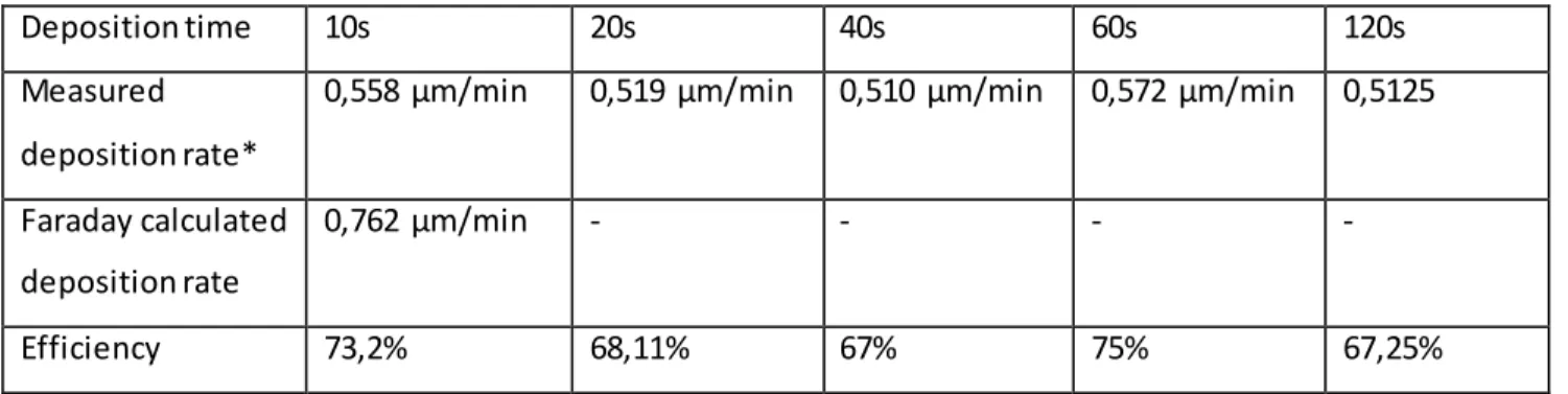
The first point was to determine a reliable deposition rate as a starting reference parameter, usi ng fixed deposition parameters, varying only time.
With a magnetic agitator set to 150 RPM, at room temperature conditions (laser thermometer showing 22,5 C° on the solution), we deposited applying 15mA/cm2 in current control and obtained the following results:
Deposition time 10s 20s 40s 60s 120s
Measured deposition rate*
0,558 µm/min 0,519 µm/min 0,510 µm/min 0,572 µm/min 0,5125
Faraday calculated deposition rate
0,762 µm/min - - - -
Efficiency 73,2% 68,11% 67% 75% 67,25%
Table 6: Parameters for deposition characterization
*: This result is obtained by scaling the effective deposited average thickness of Sn with the deposition time to obtain a rate by minute, e.g.: the thickness measured for the 10s sample was multiplied X6 as a
reasonable estimate, while the 60s sample shows the effective thickness as deposition rate per minute. Moreover, the thickness values are to be assumed, in this table and in all following references, as the result of 12 or 9 single point XRF measurements average, in order to minimise the effect the naturally uneven surface morphology of electrodeposited Sn would have on thickness evaluation.
Image 26: Graphical representation of testing patterns
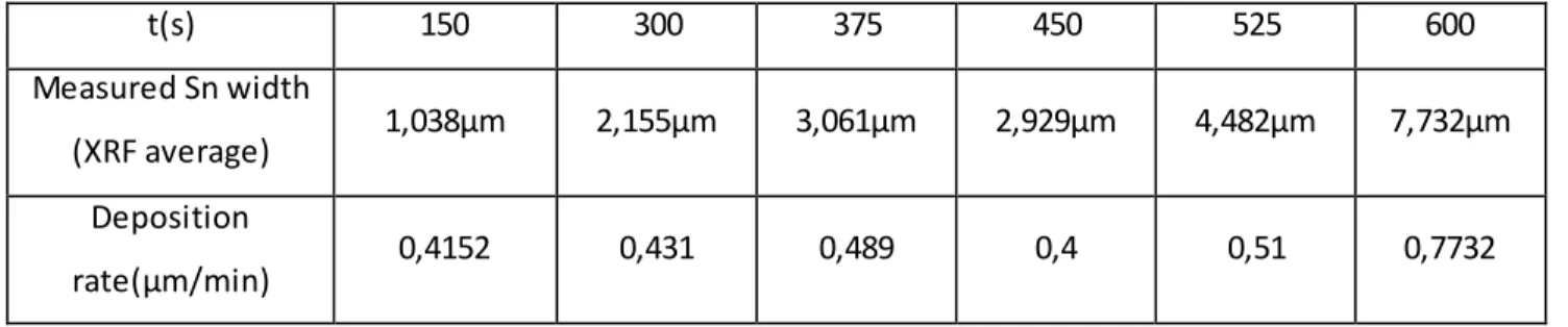
Taking these measurements into account, we obtained our fixed “point 0” in the evaluation of the deposition characterization: an estimated deposition rate, result of the average deposition rates of 12 samples (10s, 20s, 30s, 40s, 50s, 60s, 70s, 80s, 90s, 100s, 110s and 120s depositions) obtained as above shown.
This value, used as set off for the following experiments, was determined to be 0,54 µm/min. In graphs we will refer to the sample obtained under these conditions as “Sample 0”, as reference.
Gold film average width was measured in the same way to be 1,165 µm.
From this point, we started varying the parameters we could influence and recording the variations produced on the outcome.
First, we altered agitation:
For samples named as Group 21 and 22, deposition time was kept fixed at 60s, current at 15mA/cm2 and room temperature, while agitation was reduced below 100 RPM.
Plot 1: Effect of agitation on deposition rate
As we can see, even though the relative variation may appear minimal, the deposition decreased approx. 15% in samples 21 and 22. Samples 23 and 24 were deposited as reference with respectively 200RPM and 250RPM agitation.
Results show in a satisfactory way that while agitation does influence notably the outcome, above 150RPM there is no observable benefit in deposition rate.
It was however observed that the greater agitation tended to form turbulent motion in the beaker, le ading to a gradient in width coherent with the sense of rotation, leading us to settle, for all following depositions, for 150 RPM agitation. 1,165 1,038 1,15 1,162 1,161 0,53975 0,456 0,483 0,529 0,531 0 0,2 0,4 0,6 0,8 1 1,2 1,4
Sample 0 Group 21 Group 22 Group 23 Group 24
µm Au
Image 27: Graphical representation of experimental conditions
Always keeping fixed deposition time, for relatability’s sake, our next step was to alter temperature. Seeing as refrigeration wouldn’t have been neither a practical option from a setup point of view (risk of water infiltration in solution due to processes of condensation on the glassware) nor from a theoretical point of view (lower T would slow the process, while we intended to find the most efficient and reliable route), we set from room T to safely within the electrolyte operating limit of 30C°, heating the setup up to 27C° (measured through IR thermometer).
The test was performed firstly with a sub-optimal agitation (<100RPM for groups 24,25,28 and 29 ), then with the agreed optimal agitation (150RPM for groups 30 and 31).
Plot 2: Study of the effect of temperature on deposition
0,53975 0,421 0,501 0,489 0,472 0,599 0,543 0 0,2 0,4 0,6 0,8 1 1,2 1,4
Sample 0 Group 24 Group 25 Group 28 Group29 Group 30 Group 31
µm Au
The slight increase in T for groups 24-25-28-29 didn’t seem to affect the deposition rate as much as the lack of properly efficient agitation, leading to an overall decrease in the average width.
Inversely, combining proper agitation with the heightened T for samples 30-31 did marginally increase efficiency, but not to an appreciable degree.
The challenge of accurate control in laboratory conditions of the temperature of the electrolyte may lead to its degradation, so room temperature would be advised even if slightly less efficient due to its superior ease in reaction control.
Having already performed various tests and having achieved at this point a reliable understanding of the deposition process, an increase in deposition irregularities prompted us to perform a first set of more advanced tests.
The main reason was to check the morphology and the internal structures of our deposit, but also to investigate potential issues that would not be revealed by a simple width monitori ng.
We decided to start with a profilometry test, all the time continuing to produce fresh samples to be analysed in different ways.
The samples sent in for profilometry testing were the aforementioned groups 24,25,28, 29, 30, 31, and we were expecting, from known literature, visible roughness, in the order of a few hundred nm, due to grain borders and overall slightly inhomogeneous growth typical of Sn.
However the steep variations observed exceeded our worst expectations, to the point of causing the suspect that either the deposition setup may have some serious flaws, or our components had been compromised.
Image 28: Profilometry test, 500 p/mm over 4mm, shows a steep step of 1,8µm and considerable irregularity
Image 29: Profilometry test, 500 p/mm over 4mm, shows a step of over 1µm
Even though the data obtained pertaining group 24 shows two distinct points of analysis, the surface roughness was suspect, leading to further tests on the samples produced shortly after this one.
Image 30: Profilometry test, 500 p/mm over 4mm, shows expected roughness over the majority of the surface, but exhibits what may be interpreted as a spike