© Jens Eriksson, PhD in Nanoscience, Scuola Superiore of the University of Catania, 2010 a.a. 2007/2010
Università degli Studi di Catania
Scuola Superiore di Catania
International PhD
in
Nanoscience
XXIII cycle
Transport properties at 3C-SiC
interfaces
Jens Eriksson
PhD program coordinators
Tutors
Prof. Emanuele Rimini
Dr. Vito Raineri
Table of contents
Introduction ________________________________________________________ i Chapter 1
Introduction to silicon carbide ________________________________________ 1
1.1 Historical background __________________________________________________ 2 1.2 Crystal structure ______________________________________________________ 4
1.2.1 Basic building block _________________________________________________________ 4 1.2.2 Polytypism ________________________________________________________________ 4
1.3 Material properties ____________________________________________________ 9
1.3.1 Mechanical and chemical properties ___________________________________________ 9 1.3.2 Electronic properties ________________________________________________________ 9 1.3.2.1 Bandgap _____________________________________________________________ 11 1.3.2.2 Critical electric breakdown field __________________________________________ 12 1.3.2.3 Thermal conductivity __________________________________________________ 13 1.3.2.4 Saturated drift velocity and carrier mobility ________________________________ 13 1.3.3 Figures of merit for high power and high frequency devices _______________________ 14
1.4 Growth _____________________________________________________________ 16
1.4.1 Hexagonal SiC bulk growth __________________________________________________ 16 1.4.2 Hexagonal SiC epitaxial growth ______________________________________________ 16 1.4.3 3C-SiC heteroepitaxy _______________________________________________________ 17 1.4.3.1 β-α SiC heteroepitaxy __________________________________________________ 18 1.4.3.2 β-α SiC heteroepitaxy by vapor liquid solid mechanism _______________________ 19
1.5 SiC devices and applications ____________________________________________ 20 1.6 The interest in cubic silicon carbide (3C-SiC) _______________________________ 23 1.7 Defects _____________________________________________________________ 25
1.7.1 Point defects _____________________________________________________________ 26 1.7.2 Linear defects ____________________________________________________________ 26 1.7.3 Structural defects in 4H-SiC _________________________________________________ 27 1.7.4 Structural defects in 3C-SiC _________________________________________________ 28
1.8 References __________________________________________________________ 31
Chapter 2
2.1 Formation of metal-semiconductor contacts ______________________________ 39 2.2 Specific contact resistance _____________________________________________ 43
2.2.1 Determination of the specific contact resistance ρc _____________________________ 45
2.3 Ni based Ohmic interfaces to single crystal 3C-SiC __________________________ 47
2.3.1 Experimental Details ______________________________________________________ 48 2.3.2. Characterization of the 3C-SiC layers _________________________________________ 50 2.3.3. Structural evolution of the Ni/3C-SiC system upon annealing _____________________ 52 2.3.4 Electrical properties of the annealed Ni/3C-SiC system __________________________ 54 2.3.5 Comparison with contacts to 3C-SiC grown by other techniques ___________________ 57 2.3.6 Nanoscale homogeneity of the contacts related to macroscopic electrical properties __ 58
2.4 Closing remarks ______________________________________________________ 60 2.5 References __________________________________________________________ 61
Chapter 3
Nanoscale transport properties at 3C-SiC Schottky interfaces ___________ 65
3.1 Schottky barrier diodes________________________________________________ 66
3.1.1 Determination of diode parameters __________________________________________ 66 3.1.1.1 Current-voltage (I-V) measurements _____________________________________ 66 3.1.1.2 Capacitance-voltage (C-V) measurements _________________________________ 68 3.1.2 Non-ideal Schottky diode behavior in SiC ______________________________________ 70 3.1.2.1 Fermi level pinning ___________________________________________________ 71 3.1.2.2 Nanoscale inhomogeneity of Schottky barriers on SiC _______________________ 72
3.2 Rectifying contacts to 3C-SiC ___________________________________________ 73
3.2.1 Experimental ____________________________________________________________ 76 3.2.2 Non-ideal behavior of 3C-SiC Schottky interfaces _______________________________ 80 3.2.3 Structural and electrical investigation of defects ________________________________ 83 3.2.4 Influence of UV-irradiation on the nanoscale electrical properties of the 3C-SiC surface 88 3.2.5 Influence of UV-irradiation on the Au/3C-SiC Schottky interface ___________________ 90 3.2.5.1 Contact area dependence of ΦB _________________________________________ 92
3.2.6 Mechanism of SF passivation _______________________________________________ 94 3.2.7 The Pt-3C-SiC system ______________________________________________________ 97 3.2.7.1 Structural evolution upon annealing _____________________________________ 97 3.2.7.2 Electrical evolution upon annealing ______________________________________ 98 3.2.7.3 Mechanisms of electrical evolution _____________________________________ 102
3.3 Conclusion _________________________________________________________ 103 3.4 References _________________________________________________________ 105
Chapter 4
Nanoscale probing of dielectric breakdown at SiO2/3C-SiC interfaces ____ 111
4.1 Experimental _______________________________________________________ 113 4.2 Material characterization _____________________________________________ 115 4.3 Localized TDDB measurements by C-AFM ________________________________ 118 4.4 Statistical analysis of BD generation ____________________________________ 124 4.5 Causes of premature dielectric BD ______________________________________ 127
4.5.1 Structural defects and morphological features _________________________________ 127 4.5.2 Oxide charges and traps ___________________________________________________ 130
4.6 Conclusion _________________________________________________________ 136 4.7 Rerefences _________________________________________________________ 136
Conclusion and outlook ____________________________________________ 140 Curriculum vitae __________________________________________________ 144
Conferences ___________________________________________________________ 144 Publications ___________________________________________________________ 145
i
Introduction
For years it has been unclear what should be the definition of an interface in materials science. For a long time it was seen simply as the intermediate layer between two bulk materials. Interface properties were deduced by theory starting from known macroscopic material properties. To date, many materials science aspects concerning interfaces in electronic devices are unresolved, and the macroscopic performances cannot be precisely predicted from the known bulk properties of the individual constituents.
In this context, nanoscience will play a key role in accessing new groundbreaking knowledge and bringing forth emerging technologies. It seems that nanoscience is the future of science but even more the science for the future. In particular, the equipments and methodologies recently implemented allow us to change the way to approach materials science and provide new means for tuning device performances. Interface properties can now be studied at nanoscale, i.e. atomic thicknesses can be resolved.
One of the fascinating physical aspects that can be investigated at nanoscale is the properties of electronic device interfaces in cubic (3C) silicon carbide (SiC). For years this material has been believed to be a very promising wide bandgap semiconductor for power electronics, due to its predicted properties. Among the large number of SiC polytypes, 3C-SiC (or β-SiC) is the only cubic form. This polytype has several potential advantages over the more mature and better studied hexagonal α-SiC (4H and 6H), such as higher electron mobility and better stability under electrical stress. These properties make it a strong candidate material for high frequency and high power applications. However, in spite of prolonged efforts, the predicted performances have not been achieved at a macroscopic level, and thus exploiting the potential advantages of this material remains an elusive task. The aim of this thesis is to understand and overcome some of the challenges faced for device fabrication in this material, by studying the nanoscale transport properties at 3C-SiC interfaces. In this way, the non-ideal macroscopic behavior of fabricated devices can be better understood and ultimately improved.
3C-SiC epilayers are most commonly grown on silicon substrates, due to the availability of cheap production over large area wafers. However, the growth of
3C-ii
SiC on Si is complicated due to the huge lattice mismatch and thermal expansion coefficient mismatch. Recent developments in epitaxial growth have demonstrated the possibility of forming heterojunction structures by growing cubic SiC on top of hexagonal SiC substrates, enabling interesting possibilities for applications, such as devices based on a two-dimensional electron gas (2DEG) that can be formed at the heterointerface, or dual wavelength optoelectronic devices that are based only on the different stacking sequences of pure SiC. Moreover, 3C-SiC grown on hexagonal SiC substrates can have superior properties due to the next to non-existent lattice mismatch (less than 0.1 % in the growth plane). However, a special twin boundary defect called double positioning boundary (DPB) is usually observed for β-α SiC heteroepitaxy, coming from the two possible orientations of the cubic β-SiC axis on the hexagonal α-SiC basis. It has been shown that this type of defect can be suppressed by using a vapor-liquid-solid (VLS) mechanism to grow the heteroepitaxial 3C-SiC. This type of 3C-SiC can then be used as the seed for subsequent homoepitaxial growth, which is the basis for most samples discussed in this thesis.
The present thesis has been done in the framework of the MANSiC research and training network funded by the European Commission within the Sixth Framework Programme. The MANSiC project was a four-year partnership (2007-2010) between nine academic institutions and two companies spread across Europe. The scientific aim of this project was to implement a knowledge based approach to develop technology based on high quality 3C-SiC thin films or bulk material grown by members of the consortium. The knowledge based approach, trough the involvement of academic research and advanced education, was necessary to find new ideas and competences in order to break the static development in the field. The goal was then to determine many of the material properties of this polytype, for which the database is still incomplete. The project was divided into 3 interdependent scientific work-packages, devoted to material growth, characterization and realization of new devices and innovative demonstrators.
In spite of recent progresses accomplished in material growth, the cubic polytype is still fraught with large concentrations of various defects, which have so far hindered the achievement of the predicted electrical properties in this polytype. As an example, the surface morphology of 3C-SiC is usually characterized by large steps, while triangular pits and large concentrations of stacking faults are also present in the material. These defects have properties that are inherently nanoscale and that will
iii have a strong influence on the electrical behavior of the material, particularly at interfaces commonly found in electronic devices, e.g. metal-semiconductor contacts (Ohmic and Schottky), p-type-n-type (p-n junctions) or dielectric-semiconductor interfaces, found e.g. in a metal-oxide-semiconductor field effect transistors (MOSFET). Understanding the behavior of non-idealities at such interfaces will be crucial in order to predict the macroscale behavior of potential devices. To this end, characterization approaches that are able to distinguish morphological, electrical and structural features at the nanoscale are essential.
In this thesis, various experimental approaches were employed and new methodologies were implemented to study structural imperfections and the nanoscale transport properties at 3C-SiC interfaces. The material was mainly provided by the project partners. The topics include the major concerns related to the electronic transport at metal/SiC interfaces and the non ideal behavior in metal/oxide/SiC systems. Characterization techniques ranging from optical, to structural, morphological and electrical were employed in this work. Most attention will be given to scanning probe microscopy (SPM) based methodologies, able to physically probe the sample and image tip-sample interactions of morphological and electrical nature at the nanoscale. Experimental approaches employing atomic force microscopy (AFM), conductive AFM (C-AFM), and scanning capacitance microscopy (SCM) modules have been employed to study various interfaces necessary to realize structures for electronic devices.
The results that have come out of this thesis can of course also be extended to a broader and more general area of interest. Indeed, in spite of the significant progress achieved in the last decade in hexagonal SiC material quality, there are still several scientific open issues related to the basic transport properties at SiC interfaces that can affect the device performance, keeping them from reaching their theoretical limits. The practical difficulties concerning SiC are largely related to limitations on the area of the devices, in turn imposed by the existence of structural defects that are formed during the growth process. Significant efforts in fundamental research at the nanoscale are essential to better understand the carrier transport phenomena, both at surfaces and interfaces. In that sense, the findings of this study can be of interest to the community of experimentalists working with SiC in the field of electronic devices.
iv
In chapter 1, a general introduction to silicon carbide is presented, providing an overview of the properties of SiC as a wide bandgap semiconductor for power electronic devices. The crystal structure and the formation and properties of different polytypes are discussed, alongside crystal growth and the state of the art of SiC power devices. While 4H-SiC is the benchmark material for the wide bandgap scientific community, the focus is maintained on new explorations. Then the topic of investigation in this thesis is motivated, outlining the potential advantages of cubic SiC and the possibilities to fabricate novel devices in β-α SiC heterostructures. The problems faced in SiC technology development are mostly related to material defects, and this particular issue is more pressing for the cubic polytype, where the material maturity is lower. Therefore, the chapter concludes by comparing the prominent types of defects present in hexagonal and cubic SiC.
Chapter 2 discusses Ohmic contacts to 3C-SiC. Ohmic contacts play a very important role in the signal transfer between the semiconductor and the external circuitry. A contact resistance that is significant compared to that of the bulk of the device will lead to a voltage drop at the contact interface, in turn resulting in decreased efficiency due to added resistive losses.
Previous findings concerning Ohmic contacts to 3C-SiC have shown a great spread in the specific contact resistance values, pertaining to the difficulty to control the material quality. The behavior of an Ohmic contact can be directly correlated to the crystalline quality of the contacted material, and it is therefore of exceptional interest to study the properties of Ohmic contacts to the high quality, single crystalline 3C-SiC material achieved by heteroepitaxial growth onto α-3C-SiC substrates. To this end, and in order to have the widest possible comparison to literature findings, the Ohmic behavior of the Ni/3C-SiC system was studied upon high temperature annealing. Indeed, comparatively low values of the specific contact resistance were measured on contacts to single-domain 3C-SiC films grown onto α-SiC substrates by the VLS technique, hinting towards very high crystal quality.
A gradual improvement in the structural uniformity of the contact interface with increasing annealing temperature up to 950°C was observed by X-ray diffraction (XRD). It was found that nickel silicide phase formation commences at annealing temperatures above 600°C, where Ni5Si2 and Ni2Si coexist upon annealing at 750°C and 850°C. After annealing at 950°C, only Ni2Si, which is the most thermodynamically stable phase in this temperature range, was detected. Also an increased presence of carbon was observed with increasing annealing temperature.
v Indeed, the mechanism of Ohmic contact formation in Ni/SiC systems upon annealing is normally attributed to the formation of carbon clusters inside the silicide, leaving vacancies in the semiconductor which act as electron donors for SiC, thereby increasing the tunneling current. However, coupling conventional electrical techniques with C-AFM current spectroscopy and current mapping allowed the visualization of a new aspect concerning Ni-based Ohmic contacts to SiC. Specifically, an increased uniformity of the nanoscale current distribution on the contacts was observed with increasing annealing temperature, indicating that an increase of the effective contact area contributes to the improvement of the contact properties normally observed after high temperature annealing of Ni/SiC.
Chapter 3 addresses one of the biggest problems for device fabrication in 3C-SiC, i.e. the difficulty to achieve good rectifying contacts, with acceptable blocking behavior. This problem has been attributed to electrically active defects in the 3C-SiC epilayers and at the heterointerfaces. Therefore, the electrical activity of defects at 3C-SiC surfaces and how they affect metal/3C-SiC Schottky (rectifying) interfaces is the main topic of the chapter. The structure and morphology of various defects present at β-SiC/α-SiC interfaces and in the cubic epilayer were studied by AFM and transmission electron microscopy (TEM). The nanoscale electrical behavior of various defects at the contact interface and the behavior of fabricated Schottky diodes were studied by local current mapping and current-spectroscopy using C-AFM. This allowed visualization of the electrical activity of defects and their role in the electrical behavior of the material from the nanoscale to the device level.
Surface preparations and interface reactions were found to be key issues for the formation of good rectifying contacts to 3C-SiC. In particular, the electrical activity of the most pervasive extended defect in 3C-SiC, the stacking fault, can be suppressed at the (111) surface by an ultraviolet (UV) irradiation. It was demonstrated that the physical mechanism behind the passivation can be related to an oxidation/healing reaction occurring locally at these defects due to their local polarity inversion with respect to the non-polar (111) surface. The passivation led to an overall improvement in the electrical properties of fabricated diodes, showing strong reductions in the leakage currents and increased Schottky barrier heights. Indeed, combining the passivation of the stacking faults with characterization of very small diodes allowed demonstrating the possibility of fabricating almost ideal Au/3C-SiC Schottky diodes. The dependence of the Schottky barrier height on the diode area found for Au contacts could be theoretically modeled as leakage currents due to
vi
electrically active point-like defects. Further improvements were observed upon a thermal reaction between Pt and SiC that consumed a thin layer of SiC to create platinum silicide, thereby generating a “fresh” interface, away from the original SiC surface.
Due to its intrinsic material properties, 3C-SiC is a promising material for high-frequency MOSFETs. In this context, the possibility to easily grow SiO2 by thermal annealing in an oxygen ambiance gives SiC a great advantage over competing compound semiconductors. However, MOSFETs fabricated in α-SiC suffer from low inversion channel mobilities, caused by a large density of interface traps that are energetically located near the conduction band edge in hexagonal SiC. Due to the lower bandgap, these traps occupy states well inside the conduction band in the cubic polytype, where they do not affect the channel mobility. Indeed, MOSFETs with excellent on-state characteristics have been demonstrated in 3C-SiC. The challenges for MOSFET fabrication in this material are instead related to poor off-state characteristics and premature oxide breakdown.
Chapter 4 presents an investigation of the SiO2/3C-SiC interface, where the causes of the often observed premature breakdown in MOS structures were studied by electrically stressing the system using C-AFM to perform localized time-dependent dielectric breakdown measurements on „nano-MOS‟ capacitors formed at each tip position. Such an experimental approach allows direct observation of dielectric failure as a function of stress time, which can then be related to the simultaneously acquired surface morphology, all determined with nanoscale lateral resolution. A strong correlation was found between the oxide reliability and the 3C-SiC surface roughness prior to oxidation. Premature breakdown was found to occur preferentially near step-bunching edges, which was attributed to a local electric field concentration on top of these defects due to the abrupt change in height. A combination of capacitance-voltage measurements and scanning capacitance spectroscopy (SCS) characterization showed that premature breakdown not caused by structural defects at the oxide-semiconductor interface can be attributed to electron injection into traps while the SiO2/3C-SiC system is kept in accumulation.
At the end of the thesis, the scientific open points overcome in this work are summarized, reporting also which new issues that have been raised along the road. An outlook for β-α SiC heterostructures and interesting possible future investigations are also discussed.
1
Chapter 1
Introduction to silicon carbide
Silicon carbide (SiC) is a wide bandgap semiconductor with properties that are highly suitable for devices working at high-power, high-frequency, high-temperature, and in harsh environments, with superior performances compared to silicon-based devices. This well-tried opening is found in many papers on the topic of SiC. Still, it cannot be omitted, since it highlights the material‟s potential and the reason it has been a topic of intense study for several decades. SiC is a material with high breakdown electric field strength, high saturated drift velocity of electrons, and a high thermal conductivity. Moreover, SiC has a great advantage over competing compound
semiconductors in the fact that, like silicon (Si), it has silicon dioxide (SiO2) as its
native oxide. This is a key element to any semiconductor technology, both concerning processing and device applications. For example, it opens up great possibilities for device applications utilizing a metal-oxide-semiconductor (MOS) structure. Therefore, these properties make SiC ideally suited for a vast number of applications. In this chapter, more details of the promising properties as well as the material‟s challenges will be discussed. Indeed, the unique properties that have attracted so much attention to SiC also make it a challenge to manufacture and process into working devices.
The main application for SiC crystals is in power electronics. Silicon is the material currently dominating the electronics industry. However, the demand for improved energy efficiency in power electronics, which can be satisfied by reducing the switching and conduction losses of devices, as well as devices capable of high temperature operation, is pushing for the power electronics technology development in wide bandgap semiconductors. In this context, SiC has been touted as a top candidate for decades. Recently, the development of modern epitaxial techniques has led to a rapid improvement in the material quality of SiC, thus leading to a constant increase in the performances of SiC based devices.
In this way, the material is slowly moving on from being perpetually “promising”, to becoming a reality for the cutting edge power applications of today and in the future.
2
Compared with their silicon counterparts, electronic devices fabricated in SiC enable a significant reduction of the electrical losses, as well as of the sizes and weights of the electronics modules, with ensuing improvements in efficiency and cost.
The potential applications of SiC-based electronic devices nowadays include aero-space (high temperature engines, radiation hard devices), transportation (power supply, power switching and power module) as well as industry (power supply), communications (radio frequency (RF) switching) and renewable energies (e.g., power conversion in solar and photovoltaic plants).
The advantages of SiC over Si based power devices can be summarized as follows: SiC unipolar devices are thinner, and they have lower on-resistances, which
results in lower conduction losses and higher overall efficiency.
SiC based power devices have higher breakdown voltages because of their higher critical breakdown electric field.
SiC has higher thermal conductivity (4.9 W/cm-K for SiC and 1.5 W/cm-K for Si), meaning that SiC power devices have a lower thermal resistance and the device heating rate is slower, also enabling size reduction in the cooling systems of power applications.
SiC can operate at higher temperatures (up to 1000°C compared to 150°C for Si). SiC is extremely radiation hard and therefore suited for aerospace applications, by
decreasing the additional weight from radiation shielding.
Because of low switching losses, SiC based devices can operate at high frequencies (> 20 kHz) which is not possible with Si based devices in power levels above a few kilowatts.
1.1 Historical background
Silicon carbide (SiC) is a solid compound made of 50% carbon and 50% silicon. Naturally occurring SiC is also known as “moissanite”, after the French researcher Dr. Henri Moissan who first identified it in 1905 [1]. It is found only in minute quantities in exceptional geological places like kimberlitic volcanic openings and in certain types of meteorite. Virtually all of the silicon carbide sold in the world is synthetic. The first to synthesize SiC was Jöns Jacob Berzelius in 1824 [2]. Berzelius
3 was born just outside of Linköping in Sweden, which is peculiar considering that the
center of SiC research in Sweden is at the University of Linköping. However, at that
time the properties of SiC were not understood. The interest in SiC did not rise until the invention of the electric smelting furnace by Eugene and Alfred Cowles [3], and Acheson‟s adoption of this furnace to produce carbonaceous compounds to substitute
diamond as an abrasive and cutting material [4]. The crystalline products Acheson
found after the process were characterized by a great hardness, refractabiliy and infusibility. He called the product “carborundum” and described it as a carbon silicide with the chemical formula SiC. Shortly afterwards the electronic properties of SiC started to be investigated. The first light emitting diode (LED) was made from SiC in 1907 [5]. In 1955, Lely presented a new concept of growing high quality crystals. The research in SiC became more intensified after this and the first SiC conference was held in Boston in 1958. However, the success and rapid increase of the Si technology caused the interest in SiC to drop, and the SiC research activities in the 1960‟s to the late 1970‟s were scarce. The next big break came in 1978, with the invention of the seeded sublimation growth by Tairov and Tsvetkov [6] that led to the birth of SiC wafer growth. By introducing a seed crystal and forcing material transport from the source to the seed by a thermal gradient, the growth rates could be increased and seeds of larger diameters and lengths could be made. The produced boules could be sliced and polished into wafers.
In 1987, another breakthrough came with the “step-controlled epitaxy” on off-axis substrates [7], which meant that high quality epitaxy could be conducted at low
temperatures. In light of this milestone, Cree Research was founded in 1989 and
became the first company sell SiC wafers, and Cree has remained the biggest player to this day when it comes to SiC substrates. This was the beginning of a wave of interest for SiC that is yet to subside.
In 2001, Infineon launched its Schottky diode product line made from SiC (currently
in the 5th generation) and Cree also has Schottky diode as well as high-frequency
MESFETs on the market. The SiC Schottky diode market was worth an estimated
$29 million in 2009, with market revenues estimated to be 25% higher than the previous year. Moreover, limitations of the Si technology and the III/V technology have further increased the interest in SiC and at present the field is growing rapidly much owing to the recent commercial availability of substrates. In August 2010, CREE announced 6” 4H-SiC wafers. Improved epitaxy, continuously growing wafer
4
diameters and improved material quality, coupled with milestones in devices, ensures that the currently large interest will remain.
1.2 Crystal structure
1.2.1 Basic building block
Silicon carbide is a binary compound, tetrahedrally bonded and made up by Si and C atoms (both group IV element materials) in a 1:1 ratio [8,9]. Each Si atom shares electrons with four C atoms, so that each atom is 88% covalently and 12% ionically bonded to four nearest neighbors. The approximate distances between Si-C and Si-Si or C-C atoms are 1.89 Å and 3.08 Å, respectively. The basic building block of a silicon carbide crystal is the tetrahedron of four silicon atoms with a carbon atom in
the center. The SiC tetrahedron is schematically illustrated in Fig. 1.
Figure 1. Tetragonal bonding of a central carbon atom with the four nearest silicon neighbors. Two types of tetrahedrons can nucleate, where one is rotated 180° around the
c-axis with respect to the other.
1.2.2 Polytypism
In general, the phenomenon of the same material crystallizing in different modifications is called polymorphism. The existence of different crystalline modifications of SiC was discovered in 1912 [10]. However, since SiC exhibits a particular two-dimensional polymorphism, the different SiC modifications were later
5 named polytypes [11]. The various polytypes, which can exist in cubic (C), hexagonal
(H), and rhombohedral (R) crystal structures, share the same chemical composition
but exhibit different electrical properties.
All the known polytypes of silicon carbide crystallize according to the laws of close spherical packing, resulting in binary structures constituted by identical layers. All polytypes have a hexagonal frame of SiC bilayers. Viewed as layers of spheres of the same radius, the hexagonal frame takes on the shape in Fig. 2. The SiC bilayers are the same for all lattice planes. However, the relative positions of the adjacent planes are slightly shifted to fill the „voids‟ in the adjacent layer in a close-packed arrangement. Then, as seen in Fig. 2, there are three possible inequivalent positions for the spheres. Referring to the possible positions as A, B, and C, the different polytypes can be built by organizing the repetitive stacking sequence. Thus, e.g. the only cubic polytype in SiC, called 3C-SiC, has the stacking sequence ABCAB. The simplest hexagonal structure, called 2H-SiC, has the sequence ABA. The two important hexagonal polytypes, 6H-SiC and 4H-SiC, take on the sequences ABCACBABCACB, and ABCBABCB, respectively. The number in the notation refers to the number of layers before the sequence repeats itself [12].
These structures differ both in the order in which cubic (C) and hexagonal (H) layers are arranged and in the number of these layers in a unit cell. What determines the polytype is the sequencing order of the C tetrahedron during the stacking of the Si-C bilayers (see Fig. 1 and Fig. 2).
6
Figure 2. Schematic positions of atom centers for a close spherical packing. Only three possible positions exist for the SiC tetrahedron centers—A, B and C.
Fig. 2 shows schematically the positions of the SiC tetrahedron centers for a close spherical packing. If in the first layer the centers of all the spheres lie at points A, in the second layer positions of centers at points B or C are possible. If in the layer centers of all the spheres lie at points B, in the next layer positions of centers at points A or C are possible. If in the layer centers of all the spheres lie at points C, in the next layer positions of centers at points A or B are possible. In such a way the positions, which are occupied by atoms in the second and subsequent layers, determine the structure of a polytype. In other words, for each polytype the structure will simply correspond to the letters‟ sequence AB, ABC, ABCB, etc. Polytypes are also frequently characterized by Ramsdell designations [13], constituted by a natural number, equal to the number of layers in the period in the direction perpendicular to the basal plane, and a letter symbol characterizing the crystal system of the Bravais lattice: C, cubic; H, hexagonal; R, rhombohedral. The most frequently occurring are 6H, 4H, 15R and 3C polytypes (see optical images in Fig. 3).
7
Figure 3. Optical images of the four most common SiC polytypes.
Figure 4. Schematic images of the hexagonal and cubic crystal lattices of SiC [13].
The hexagonal and cubic crystal lattices are schematically shown in Fig. 4. Only in two SiC polytypes, the positions of all atoms are equivalent and correspond to either cubic (3C-SiC) or hexagonal (2H-SiC) sites of the crystal lattice (4H-SiC has one cubic and one hexagonal and 6H-SiC has two cubic and one hexagonal) [14]. In all other polytypes, atoms may occupy sites of both types and polytypes differ in the number of atoms in hexagonal (NH) and cubic (NC) positions (see e.g. [15]).
8
Therefore, it is convenient to characterize polytypes of silicon carbide by the parameter „hexagonality‟ γ [16], which is defined as the ratio between the number of atoms in hexagonal positions and the total number of atoms in the unit cell:
C H H N N N (1)
The hexagonality of a polytype may vary from unity (2H-SiC) to zero (3C-SiC). It is noteworthy that the ability to crystallize in different crystal lattices is inherent not only in SiC, but also in quite a number of other compounds: GaN, ZnSe, ZnO, diamond, etc. However, these other compound semiconductors normally crystallize only in the 3C and 2H polytypes, without the intermediate polytypes. By contrast, the extreme polytypes are more difficult to obtain for SiC, whereas this compound crystallizes in a plentitude of intermediate forms. 3C-SiC films of a rather large area have been obtained (see e.g. [17] or [18]), whereas 2H crystals exist at present only in the form of needles [19]. The absence of crystals with sizes suitable for device applications means that most of the electrical parameters of 2H-SiC have not been determined.
At present, there is no theory that would be satisfactory in every respect in explaining why SiC crystallizes in a wide variety of polytypes. It is not completely clear, either, what factors favor formation of one or another polytype.
A remarkable and beautiful feature of polytypism is the behavior of impurity atoms. In Fig. 5, it can be seen that the sites are not equivalent in the hexagonal polytypes 6H-SiC and 4H-SiC. The difference is in the second-nearest neighbors. A nitrogen atom substituting a carbon atom in the lattice can either occupy a “k” site or an “h” site in 4H-SiC. The k site is a lattice site that displays cubic symmetry, whereas the h site has hexagonal symmetry. The immediate vicinity of a nitrogen atom on either site is the same, but the second-nearest neighbors to the sites are different, which creates a slightly different core binding energy. Thus, 4H-SiC has two binding energies for the nitrogen donor, which has consequences when designing devices. 6H-SiC has three energy levels for nitrogen and 3C-SiC has only one. More complex polytypes such as rhombohedral (15R-SiC) have no less than five binding energies, although only four have been identified [12].
9
Figure 5. The three most common polytypes in SiC viewed in the [1120] plane. From left to right, 3C-SiC, 4H-SiC, and 6H-SiC; k and h denote cubic and hexagonal crystal symmetry
points, respectively.
1.3 Material properties
1.3.1 Mechanical and chemical properties
SiC is a very hard material with a Young‟s modulus of 424 GPa [20]. It is chemically inert and reacts poorly (if at all) with any known material at room temperature. The only known efficient etch at moderate temperatures is molten KOH at 400 - 600°C. It also has no liquid phase and instead sublimes at temperatures above 1,800°C. The
vapor constituents during sublimation are mainly Si, Si2C, and SiC2 in specific ratios,
depending on the temperature.
1.3.2 Electronic properties
While the possibility to crystallize in different polytypes, being chemically inert, hard, and temperature resistant are all important properties, the aspect of SiC that has attracted so much attention concerns the unique electronic properties.
10
Due to the unstable nature on most polytypes, only three of them are commonly produced. They are called 6H-SiC, 4H-SiC and 3C-SiC. Most of the physical properties of these polytypes are identical, except the electronic ones. The main parameters of 6H, 4H and 3C SiC polytypes are listed in table 1. For electronic devices, each polytype has its specific advantages. For example, 4H is better suited for high power (e.g. high voltage electricity distribution) and high temperature (e.g. car or plane engines), while 3C should be better for high frequency applications (e.g. radar).
Table 1. Selected physical and electronic properties of the most common SiC polytypes [21].
Parameter 4H-SiC 6H-SiC 3C-SiC
Stacking order ABCB ABCACD ABC
Jagodzinskii notation hc hcc c Percentage ‘hexagonality’, γ (%) 50 33 0 Lattice constant (Å) a = 3.073 c = 10.053 a = 3.08 c = 15.117 4.34 Dielectric constant, ε 9.66 9.66 9.72 Bandgap (eV) 3.26 3.0 2.39 Thermal conductivity (W cm−1 °C−1) 3-4 3-4 3-4 Critical breakdown field strength, Ec (MV cm−1) 3 3 2 Electron mobility, μn (cm2 V−1 s−1) (300 K) ≤ 850 ≤ 450 ≤ 1000 Saturation rate, vs (× 107 cm s−1) 2 2 2.7 Hole mobility, μp (cm2 V−1 s−1) (300 K) ≤ 120 ≤ 100 ≤ 40
11
1.3.2.1 Bandgap
The wide bandgap is what enables the use of SiC for very high temperature operation. Thermal ionization of electrons from the valence band to the conduction band, which is the primary limitation of Si-based devices during high temperature operation, is not a problem for SiC-based devices because of this wide bandgap.
The band structure is indirect, and the width of the bandgap strongly depends on the polytype; specifically, it depends on the percentage of hexagonality (γ from Eq. 1), and varies from 2.39 eV for 3C-SiC to 3.33 eV for 2H-SiC [21]. Thus, the difference in the bandgaps (ΔEg[H–C]) between the cubic (3C) and the purely hexagonal (2H) polytypes of SiC is 0.9 eV. The bandgap is plotted as a function of γ in Fig. 6. For other semiconductors exhibiting different polytypes (GaN, ZnS, ZnSe, etc), ΔEg[H–C] is generally≤ 0.2 eV [22]. 0 20 40 60 80 100 2,2 2,4 2,6 2,8 3,0 3,2 3,4 2H 4H 15R 33R 6H 8H 21R Eg ( e V) (%) 3C
Figure 6. Energies of the indirect bandgap of several SiC polytypes as a function of the ‘hexagonality’ percentage [23].
12
1.3.2.2 Critical electric breakdown field
One of the most important properties for power-device applications is the critical
electric breakdown field, EC. This property determines maximum electric field that
the material can support before suffering physical breakdown. Normally, wide
bandgap materials have a high breakdown electric field because the wide bandgap leads to high impact ionization energy. Silicon carbide can withstand an electric field about ten times greater than GaAs or Si without undergoing avalanche breakdown [24]. This high breakdown electric field enables the fabrication of very high-voltage, high-power devices such as diodes, power transistors or high power microwave devices [25]. In addition, it allows close distances between adjacent devices, allowing high device packing density for integrated circuits. The breakdown voltage at a p-n junction is given by:
2 d C B W E V (2)
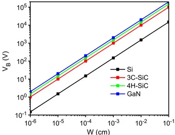
where VB is the breakdown voltage, and Wd the drift region width. Considering the same breakdown voltage, a significantly thinner drift region can be realized in SiC compared to Si. In Fig. 7, VB is shown as a function of the drift region width for different materials. 10-6 10-5 10-4 10-3 10-2 10-1 10-1 100 101 102 103 104 105 V B (V) W (cm) Si 3C-SiC 4H-SiC GaN
Figure 7. Breakdown voltage as a function of drift region width for Si, 3C-SiC, 4H-SiC and GaN.
13
The relative strength of EC for SiC compared to Si of ten times refers to devices
designed for the same blocking voltage. For a doping of approximately 1016 cm−3, EC
for 4H-SiC is 2.49 MV/cm [26]. For Si, the value of EC is about 0.401 MV/cm for the
same doping [27]. In this comparison, the difference between SiC and Si is only about a factor of six and not the often advertized factor of ten. However, if one compares the critical strengths of devices made for the same blocking voltage, then a Si device constructed for a blocking voltage of 1 kV would have a critical field strength of about 0.2 MV/cm, which, when compared with the 2.49 MV/cm of SiC, amounts to the factor of ten.
1.3.2.3 Thermal conductivity
The second most important parameter for high power and high-frequency device applications is the material‟s thermal conductivity. An increase in temperature generally leads to a change in the physical properties of the device, which normally affects the device in a negative way. Most important is the carrier mobility, which decreases with increasing temperature. Heat generated through various resistive losses during operation must thus be conducted away from the device and into the package.
At room temperature, SiC has a higher thermal conductivity than any metal. The thermal conductivity of copper is 4.0 W/(cm-K) [28]. That of silver is 4.18 W/(cm-K) [28]. There is a dependence on the purity of the crystal as well as on the crystal direction [29]. High-purity semi-insulating SiC material has the highest reported thermal conductivity with a value of 4.9 W/(cm-K). Lower values are measured for the doped materials but the values remain above 4 W/(cm-K) at room temperature [30]. This property enables SiC devices to operate at extremely high power levels [31,32] and dissipate large amounts of excess generated heat, which causes a temperature increase that degrades the device performance [33,34]. Due to this, together with the low power losses and the high temperature capability [35,36], SiC devices can operate without thermal cooling system contrary to other semiconductor devices, such as Si. It is a great advantage in relation to cost, size and weight of power electronic systems.
1.3.2.4 Saturated drift velocity and carrier mobility
For high-frequency devices, a very important parameter is the saturated drift velocity vs. It is one of the key material and device properties that determine the ultimate limit
14
of speed of response and frequency of a device, such as a transistor. In a semiconductor, carrier velocity cannot indefinitely increase with the applied electric field. Carriers speed up in response to a stronger field until the saturation drift velocity is reached. At this point, higher fields do not result in any increase.
In SiC, the saturation drift velocity is 2-2.7 × 107 cm/sec [37], which is at least twice that of Si. A high-saturated drift velocity is advantageous in order to obtain as high channel currents and high frequencies as possible, and clearly SiC is an ideal material for high-gain, and high-speed solid-state devices.
Electrons and holes are accelerated by electric fields, but they lose momentum as a result of various scattering processes, such as lattice vibrations (phonons), impurity ions, crystal defects, surface or other material imperfections [38]. The drift velocity vd
of a carrier is proportional to the electric field E, provided that vs has not been
reached. The mobility μ is defined as the proportionality factor between vd and E as
vd E (3) The effects of all several microscopic phenomena are lumped into the macroscopic mobility introduced in the transport equations. The mobility is dependent on the local electric field, lattice temperature, doping concentration, polytype, crystal quality, local scattering at defects, etc. If the doping concentration increases, the mobility decreases due to scattering. For low doping concentration, the mobility decreases with temperature due to decreased vibrational energy of the lattice phonons [39,40].
1.3.3 Figures of merit for high power and high frequency devices
Owing to its wide bandgap, high heat conductivity and pronounced thermal, chemical and radiation stability, SiC has been regarded primarily for applications in the field of power electronics. The device potential of a semiconductor material is often estimated in terms of figures of merit. Johnson‟s figure of merit (JFOM) addresses the potential of a material for high frequency, voltage and power discrete amplifiers, according to [41]
2 2 2 4 s B E JFOM v (4) where EB is the breakdown electric field and vs is the electron saturation velocity. The15 Key‟s figure of merit (KFOM) instead considers the potentiality of a material for high frequency applications (like MOSFETs) [42]:
4 s c KFOM v (5) where κ, c, and ε are the thermal conductivity, the speed of light in vacuum, and the dielectric constant, respectively. Neither of these merits accurately describes the
potential for power devices. Baliga‟s figure of merit (BFOM) [43] defines parameters
to minimize the conduction loss in low-frequency applications:
BFOM EB3 (6) where μ is the carrier low-field mobility. In Table 2, the figures of merit are presented for n-type 3C-SiC, 4H-SiC, diamond [44], GaN [45], GaAs [45] and Si [45]. All
values are normalized to Si. It seems that 3C-SiC is the best SiC option for high
frequency switching, inferior only to diamond among these materials. By studying Table 2 it is clear that, from a purely theoretical point of view, diamond would be the ultimate semiconductor for power electronics. However, it should be mentioned that the figures of merit do not tell the whole story. In diamond, the energy levels of the dopants are much deeper than those in SiC, leading to poor operation at room temperature. There are also other problems related to the use of diamond that appear to be even larger than the problems faced by the SiC technology community [46].
Table 2. Relative figures of merit of different semiconductors.
JFOM KFOM BFOM
Si 1 1 1 3C-SiC 324 4.83 163 4H-SiC 400 4.17 464 GaAs 1.78 0.32 14.6 GaN 1600 3.04 1507 Diamond 8,100 32.2 23,000
16
1.4 Growth
While it is beyond the scope of this chapter and this thesis to explain the details of SiC growth, the main principles of commercial bulk and epitaxial growth of hexagonal SiC will be summarized here. The specific growth of heteroepitaxial 3C-SiC on α-3C-SiC substrates will also be discussed, since it is more essential to the topic of this thesis.
1.4.1 Hexagonal SiC bulk growth
Silicon carbide substrates are the key elements in the development of SiC epitaxial layers for electronic devices. Because of the phase equilibriums in the Si and C materials system (the material sublimes before it melts), the most popular bulk growth techniques are based on physical vapor transport. As previously mentioned in Section 1.1, Tairov and Tsvetkov [6] invented seeded sublimation growth in 1978. The techniques used today to manufacture SiC wafers are almost exclusively based on this concept. In this technique, a seed crystal of SiC is introduced into the reactor chamber and heated above the sublimation temperature. A thermal gradient is applied
so that the seed is slightly colder than the source. Vapor transport of carbon and
silicon bearing species from the source (or carbon species from the graphite walls)
will thus occur to the seed where it condenses and the growth proceeds (usually along
the c-axis). The principal vapor constituents during sublimation are Si, Si2C, and
SiC2, and the ratio between them depends on the temperature. For a typical 4H-SiC
bulk sublimation growth process, the SiC source temperature is 2100-2400°C [47].
1.4.2 Hexagonal SiC epitaxial growth
In order to improve the quality compared to the bulk material and to produce complex device structures, epitaxial techniques are necessary. Epitaxial layers are needed in all electronic SiC applications and their characteristics are mainly dependent on the intended final device. For example, power devices (from few hundred volts to some kilovolts) typically require low-doped (1014-1016 cm-3) and thick (5-100 μm) layers, whereas high-frequency devices require thin layers (less than 0.2 μm to several μm) with moderate (1016 cm-3) to heavy (1019 cm-3) doping.
Chemical vapor deposition (CVD) is presently the most widely used epitaxial technique for growth of SiC epitaxial layers for device structures. The basic steps occurring during CVD can be listed as follows (Fig. 8): reactant gases are transported
17 by carrier gas to the reactor, reactant species diffuse through the boundary layer above the growth surface, reaction (adsorption or chemisorption) takes place on the surface, gaseous byproducts are transported away from the surface, they diffuse away through the boundary layer and are eliminated with the carrier gas [48-50].
There are several types of CVD reactors, e.g. vertical or horizontal, cold wall or hot wall, made of metal or quartz, working at atmospheric or low pressure, with or without plasma, with different heating types. The wafer is positioned on a resistively or inductively heated substrate holder and fed by a mixture of reactants, for SiC typically SiH4 + C3H8 diluted in H2.
Figure 8. Schematic of the fundamental steps involved during chemical vapor deposition [50].
Thanks to the massive progress achieved in SiC epitaxial growth in the last 25 years, it is now possible to grow high-quality epilayers on the bulk substrates. This progress has enabled the fabrication of virtually all types of semiconductor devices using SiC technology, as will be discussed in 1.5.
1.4.3 3C-SiC heteroepitaxy
All of the material used in this thesis started with a 3C-SiC layer that was heteroepitaxially grown onto some underlying substrate. Indeed, for 3C-SiC no real bulk growth exists, and the material is grown by heteroepitaxy onto Si or α-SiC substrates. This leads to the classical heteroepitaxial problems such as mismatch induced defects, interfacial reactivity and wafer bending [51].
18
Many attempts have been performed in order to grow high quality crystalline 3C-SiC films on Si substrates, but the huge lattice mismatch (20%) between Si (5.43 Å) and 3C-SiC (4.53 Å) and the large difference in thermal expansion coefficients (8%) lead to large stresses in the grown film [52]. This results in a poor crystalline quality of 3C-SiC and, consequently, in poor device characteristics.
1.4.3.1 β-α SiC heteroepitaxy
Growing 3C-SiC heteroepitaxially onto 6H-SiC or 4H-SiC could lead to an improvement of the crystalline quality of the cubic polytype, due to an almost negligible lattice mismatch (0.1%) between 3C-SiC and α-SiC [21]. The 0.1% lattice mismatch may seem strange if one considers the lattice parameters specified in table 1. However, in order to conceive how the cubic lattice is incorporated into the hexagonal one, it is necessary to look from above at a cube standing on one of its vertices. The projection of such a cube onto a horizontal plane will be a hexagon, as seen in Fig. 9. In this case, a growing 3C-SiC film will have another crystallographic orientation than that of the substrate. If the initial hexagonal substrate has a (0001) orientation, the grown 3C-SiC layer will have a (111) orientation. This means that the lattice constants of the cubic and hexagonal polytypes virtually coincide in the growth plane (lattice mismatch < 0.1%).
During the initial stacking of 3C-SiC on the (0001) hexagonal plane, two equally probable nucleation orientations (differing by a 60° rotation) are possible, as can be seen in Fig. 9. When 3C-SiC islands of different orientation nucleate and subsequently expand and meet during growth, the individual domains are separated by extended defects known as double-positioning boundaries (DPBs) [53]. We will see in chapter 3 that this type of defect provides a local path for leakage currents to pass through the 3C-SiC layer, and they have a particularly deleterious influence on the rectifying properties of metal-3C-SiC contacts.
19
Figure 9. Incorporation of the cubic lattice onto the hexagonal SiC substrate.
1.4.3.2 β-α SiC heteroepitaxy by vapor liquid solid mechanism
In addition to CVD grown SiC heterostructures, 3C-SiC grown on α-SiC by a so called Vapor-Liquid-Solid (VLS) technique have been used for this thesis. A home-made deposition apparatus at the Université Claude Bernard, in Lyon, France, specially designed for VLS growth, was used. A schematic of the reactor is presented in Fig. 10. Briefly, the α-SiC (0001) on-axis or 2° off-axis seeds are placed at the bottom of a graphite crucible. Si and Ge pieces are then stacked on top of the seed and heated under purified Ar up to 1200-1450°C in order to form alloy melts containing various atomic % of Si. Propane is added at high temperature to start the VLS growth. The optimized use of this technique has been found capable of suppressing the DPB defects normally observed for β-α SiC epitaxy [53].
20 optical pyrometer vent pump manual valve Pneumatic valves Mass flow controller
Induction coils graphite tube SiH 4 Ar C3 H8 MFC3 MFC1 MFC2 evacuation stainless steel aspiration tube pump vent Water cooled reactor
Figure 10. Schematic of the VLS equipment.
1.5 SiC devices and applications
The mainstream electronics of today has evolved over the last five decades through continuous developments of the silicon technology. Even if other semiconductors, like SiC, are emerging and displaying superior bulk properties compared to silicon, their role remains limited to niche markets. However, the dramatic and rapid development of silicon technology would not have happened if it had been locked in a race against the pre-existing technologies at that time, competing for the same applications (like vacuum tubes for signal amplifiers). Similarly, no remarkable development of SiC electronics should be expected if the efforts are limited to a competition with silicon for existing applications. So, how can SiC technology become attractive and competitive in the electronics market? A long chain of new applications cannot be created at the same level of sophistication or system complexity as in silicon technology, at least not in a foreseeable time. However, the extraordinarily high levels of complexity of integrated electronic systems, the
21 nanosized structures, and the highly sophisticated functions are pushing Si technology ever closer towards its physical limitations. As such, the electronics community is pushed toward the development of new technologies in other materials. The demand for low switching and conduction losses, as well as devices capable of high temperature operation is a major driving force behind power electronics technology development in wide bandgap semiconductors. The development of modern epitaxial techniques has lead to a rapid improvement in the material quality of silicon carbide, with the consequence that SiC devices have now become an interesting reality.
SiC technology surely opens up the possibility of a new generation of electronic equipment offering more effective, smaller and cheaper solutions. Actually, the conditions to make SiC the foremost semiconductor material for high temperature, high voltage, high frequency and high power applications exist [54,55]. It can be used in a large number of industrial and military areas and, in particular, in the harshest environments, such as nuclear reactors and space.
Because SiC has a critical electric breakdown field strength that is about ten times larger than that of Si, SiC power electronic devices can be made much thinner than the corresponding devices based on Si. Coupling this with the capability to handle larger current densities, SiC devices can be made smaller and more efficient. Also, because the thermal conductivity of SiC is approximately three times higher than that of Si, the size of power electronic devices can be further reduced in the cooling systems. Thus, the future of SiC technology looks very promising thanks to its smaller size, lower power losses, higher efficiency, and better heat-dissipation. Comparing the properties of silicon carbide to some other semiconductors, one notes that SiC is superior in many regards. For example, the existing semiconductor technologies of Si and GaAs cannot tolerate high temperatures and chemically hostile environments, while the large Si-C bonding energy makes SiC resistant to high temperature, chemical attack and radiation. Most traditional integrated circuit technologies using silicon devices are not able to operate at temperatures above 150°C, especially when high operating temperatures are combined with high-power, high-frequency and harsh environment. High-temperature circuit operation from 350°C to 500°C is desired for use in aerospace applications (turbine engines), nuclear power instrumentation, satellites, and space exploration. These are environments and applications where SiC may really come to shine.
22
It is now clear that a change in technology from silicon to silicon carbide will revolutionize the power electronics. For instance, it will be economically feasible to use power electronics to a much larger extent than today. High power silicon carbide devices which operate at high temperatures will be used for a variety of power applications, e.g. in space-based, light-weight and radiation hard power systems, electric airplanes, military electric vehicles, engine control in new hybrid cars, and turbine engine actuators. Many of these applications require diodes and switches capable of blocking large voltages and conducting large currents, while operating at elevated temperatures and being subjected to harsh environments.
So far, a wide array of SiC devices has been experimentally demonstrated, including bipolar junction transistor (BJT). [56], insulated gate bipolar transistor (IGBT) [57],
metal-semiconductor-field effect transistor (MESFET) [58], junction field effect
transistor (JFET) [59] and metal-oxide-semiconductor field effect transistor (MOSFET) operating at temperatures up to 923 K [60], p-n junction diodes and Schottky diodes [61]. Additionally, heterojunction devices such as GaN/SiC heterojunction bipolar transistor (HBT) have been produced [62].
Looking at the power electronics market, today there are high-frequency JFETs offered commercially, as well as an emerging market for Schottky diodes made from
SiC available from Cree, Infineon and ST microelectronics. Schottky diodes
fabricated in 4H-SiC have been shown to have superior performance compared to Si-based devices. Due to SiC´s outstanding material properties, unipolar SiC Si-based electronic devices show lower switching losses, combined with higher switching speeds and they also show better thermal stability. With the commercialization of silicon carbide diodes starting almost one decade ago (Infineon released its first generation of SiC Schottky diodes in 2001), today the SiC diode product line boasts a voltage range from 300 V up to 1700 V [59].
Considering the market for SiC, that of Schottky diodes is currently the largest, and it is continuously growing. Presently, the largest portion of these devices is used for power supply applications. However, many industry experts believe that the largest market for SiC Schottky diodes within the next years will be photovoltaic inverters for solar cells and photovoltaic plants, where the possibility to increase the efficiency of the inverter modules can lead to considerable savings in cost.
While SiC JFETs are becoming available on the commercial market they have not yet succeeded to the same extent. Furthermore, within this year some semiconductor companies announced the release of the first SiC MOSFETs and BJTs in late 2010.
23 Clearly, the future of this material seems to be bright. We are still at an early stage of the SiC revolution, however, and the material‟s full potential has yet to be realized. Aside from the power device market, SiC has also found its way into the fields of radiation detectors and chemical sensors. SiC has proved to be efficient at absorbing short wavelength light, which has enabled the realization of SiC UV-sensitive photodiodes, including commercial UV flame detectors made by General Electric
[63]. By monitoring and controlling the combustion gas-fired turbines used in
electrical power generation systems, these UV flame sensors are reducing pollution emissions. Also high quality prototypes of other devices have been demonstrated, such as large-area SiC X-ray detectors based on Schottky diodes, which function at 100°C [64].
The high-temperature capabilities of SiC allow the production of catalytic metal-SiC and metal-insulator-SiC (MIS) structures used as gas sensors. The wide bandgap of silicon carbide permits an operation temperature of up to 1,000°C [65], with time
constants for the gas response of a few milliseconds [66]. The high possible operating
temperature of these devices, not possible with silicon, favors their use in combustion engines, where they could assist in active combustion control, reducing pollution emission from automobile and aircraft engines.
1.6 The interest in cubic silicon carbide (3C-SiC)
First of all, 3C-SiC is the only polytype with isotropic properties due to its cubic crystal symmetry. In addition, it is not subjected to micropipe defects formation. 3C-SiC has a larger saturated drift velocity than both 4H- and 6H-3C-SiC polytypes, and more than twice that of Si, which is advantageous for obtaining higher channel currents in microwave devices [12].
Furthermore, among the three most stable SiC polytypes, 3C-SiC has the highest bulk electron mobility. The carrier mobility influences the frequency response or time response behavior of a device in two ways. First, the mobility is proportional to the carrier velocity for low electric field. Therefore, a higher mobility material is likely to have a higher frequency response, because carriers can move more readily through the device. Second, the device current depends on the mobility; i.e. higher mobility results in larger currents. At larger currents, the capacitance charges faster, leading to a higher frequency response [67].
![Figure 4. Schematic images of the hexagonal and cubic crystal lattices of SiC [13].](https://thumb-eu.123doks.com/thumbv2/123dokorg/4533774.35427/19.918.155.733.347.707/figure-schematic-images-hexagonal-cubic-crystal-lattices-sic.webp)
![Table 1. Selected physical and electronic properties of the most common SiC polytypes [21]](https://thumb-eu.123doks.com/thumbv2/123dokorg/4533774.35427/22.918.171.790.352.891/table-selected-physical-electronic-properties-common-sic-polytypes.webp)
![Figure 6. Energies of the indirect bandgap of several SiC polytypes as a function of the ‘hexagonality’ percentage [23]](https://thumb-eu.123doks.com/thumbv2/123dokorg/4533774.35427/23.918.216.626.447.752/figure-energies-indirect-bandgap-polytypes-function-hexagonality-percentage.webp)
![Figure 8. Schematic of the fundamental steps involved during chemical vapor deposition [50]](https://thumb-eu.123doks.com/thumbv2/123dokorg/4533774.35427/29.918.209.676.334.591/figure-schematic-fundamental-steps-involved-chemical-vapor-deposition.webp)
![Figure 11. Energy band diagram at the 6H-SiC/3C-SiC heterointerface in the case of n-type material [72]](https://thumb-eu.123doks.com/thumbv2/123dokorg/4533774.35427/37.918.218.668.133.380/figure-energy-band-diagram-sic-sic-heterointerface-material.webp)

![Figure 14. HRTEM image showing misfit dislocations at the SiC/Si interface and stacking faults in the SiC layer (a), and dark field image of APBs forming at the interface (b) [91]](https://thumb-eu.123doks.com/thumbv2/123dokorg/4533774.35427/41.918.196.686.480.730/figure-hrtem-showing-dislocations-interface-stacking-forming-interface.webp)

![Figure 2. Dominating electron conduction mechanism across a metal contact to n-type semiconductors for low (a), high (b) and intermediate (c) doping concentrations [6]](https://thumb-eu.123doks.com/thumbv2/123dokorg/4533774.35427/55.918.134.746.127.391/figure-dominating-electron-conduction-mechanism-semiconductors-intermediate-concentrations.webp)
