Research Article
A Data-Flow Soft-Core Processor for Accelerating
Scientific Calculation on FPGAs
Lorenzo Verdoscia
1and Roberto Giorgi
21Institute for High Performance Computing and Networking, CNR, 80131 Naples, Italy
2Department of Information Engineering and Mathematics, University of Siena, 53100 Siena, Italy
Correspondence should be addressed to Lorenzo Verdoscia; [email protected] Received 23 December 2015; Revised 8 March 2016; Accepted 27 March 2016
Academic Editor: Zoran Obradovic
Copyright © 2016 L. Verdoscia and R. Giorgi. This is an open access article distributed under the Creative Commons Attribution License, which permits unrestricted use, distribution, and reproduction in any medium, provided the original work is properly cited.
We present a new type of soft-core processor called the “Data-Flow Soft-Core” that can be implemented through FPGA technology with adequate interconnect resources. This processor provides data processing based on data-flow instructions rather than control flow instructions. As a result, during an execution on the accelerator of the Data-Flow Soft-Core, both partial data and instructions are eliminated as traffic for load and store activities. Data-flow instructions serve to describe a program and to dynamically change the context of a data-flow program graph inside the accelerator, on-the-fly. Our proposed design aims at combining the performance of a fine-grained data-flow architecture with the flexibility of reconfiguration, without requiring a partial reconfiguration or new bit-stream for reprogramming it. The potential of the data-flow implementation of a function or functional program can be exploited simply by relying on its description through the data-flow instructions that reprogram the Data-Flow Soft-Core. Moreover, the data streaming process will mirror those present in other FPGA applications. Finally, we show the advantages of this approach by presenting two test cases and providing the quantitative and numerical results of our evaluations.
1. Introduction
There is still a slight inclination of part of the High-Performance Computing (HPC) community to embrace the data-flow ideas in order to speed up the execution of scientific applications. The reasons are mostly of a pragmatic nature rather than technical [1–4]. A dominant reason why the HPC community and, in particular, the applications programmers do not pay more attention to the advanced data-flow archi-tecture ideas is due to the fact that, in the past, very high-performance data-flow systems of commercial grade were not readily available on the market. Simulations and relatively low speed, low density academic prototype, and performance inefficiencies did not make data-flow architectures attractive to computational scientists [5, 6] because they did not offer the opportunity to application programmers to run their problems faster than before. However, despite general scepti-cism for past disappointing results, it is coming out that data-flow systems are still a valid manner to increase performance [1]. These systems, employing Field Programmable Gate
Array (FPGA) (readily available on the market, nowadays [7]) to implement data-flow accelerators, outperform most of the TOP 500 supercomputers not being paradoxically included in the list [8–10]. This happens because the (re)configurable computing paradigm offers a performance of custom hard-ware and flexibility of a conventional processor [11–13]. Because of this flexibility and the intellectual property availability, the (re)configurable approach does not only significantly accelerate a variety of applications [14] but also constitutes a valid execution platform to form programmable high-performance general purpose systems [15]. In particu-lar, given its fine grain nature, the static data-flow execution model is promising when applied to this platform [3, 16, 17].
Spatial reconfigurable computing, such as FPGAs, mas-sively parallel systems based on soft-cores, coarse-grained reconfigurable arrays (CGRAs), and data-flow-based cores, accelerates applications by distributing operations across many parallel compute resources [18]. Nowadays, FPGAs constitute a formidable tool for prototyping more complex reconfigurable and general purpose soft-cores, where the
most recent ones not only incorporate Digital Signal Pro-cessor (DSP) capabilities but also address the interconnect issue, the number one bottleneck to system performance at advanced nodes, although FPGAs continue to retain their primary characteristic of being bit-programmable.
The use of soft-core processors in building parallel systems brings in many advantages such as flexibility, the possibility to be synthesized almost for any given target Application-Specific Integrated Circuit (ASIC) or FPGA technology, the possibility to describe functions through higher abstraction levels, by using an Hardware Description Language (HDL), and many more. However, compared to custom implementations, soft-cores have the disadvantages of larger size, lower performance, and higher power con-sumption [19].
CGRAs ([15, 18, 20] give noteworthy surveys) consist of reconfigurable processing elements (PEs) that implement word-level operations and special-purpose interconnects retaining enough flexibility for mapping different applica-tions onto the system. The reconfiguration of PEs and inter-connects is performed at word-level too. CGRAs offer higher performance, reduced reconfiguration overhead, better area utilization, and lower power consumption [21] compared to fine-grain approaches. However, CGRA architectures present several limits. Firstly, because they mainly execute loops, CGRAs need to be coupled to other cores on which all other parts of the program are executed. In some designs, this coupling introduces run-time and design-time overhead. Secondly, the interconnect structure of a CGRA is vastly more complex than that of a Very Long Instruction Word (VLIW). Finally, programmers need to have a deep understanding of the targeted CGRA architectures and their compilers in order to manually tune their source code. This can significantly limit programmer productivity [22].
In the past, Miller and Cocke [11] proposed a new class of configurable computers, interconnection mode and search mode. In contrast with a von Neumann-based machine, these machines configured their units to execute the natural and inherent parallelism of a program after exposing it like a data-flow graph. Because of their configurable unit organizations, the configurable search and interconnection modes have constituted the basic models of data-flow machines [23]. Although there are several data-flow architectures proposed, most of them fall into the search mode configurable [24]. Overall, only one can be classified as partially of the inter-connection mode type and as partially of the search mode type [25]. Differently, the Data-Flow Soft-Core processor falls into the interconnection mode configurable machines. Our approach differs from strengthened reconfigurable comput-ing. For example, in a CGRA, once mapped, a data-flow graph is executed like what happens in a data-flow schema [26] by means of the associated control flow; in an FPGA, the loading of a new data-flow graph needs a configuration bit-stream that requires, at best (partial reconfiguration), at least a delay
of tenths of𝜇s [27]. Conversely, in our case, not only data
actually flow among actors without any associated control flow through a custom crossbar-like interconnect, but also the full reconfiguration time, for a new data-flow graph, requires only a delay of a few dozen ns [17].
While configurable computing has revealed its effec-tiveness over parallel systems based on conventional core processors [1], how to efficiently organize resources available at 14 nm technology or less, in terms of programmability and low power consumption, remains an open question [28]. Here we discuss a new concept of soft-core that can be effectively and efficiently supported by FPGAs with adequate intercon-nect resources called the “Data-Flow Soft-Core” (hereinafter DFSC) processor.
The idea is to make available, on a reconfigurable chip, a processor that accelerates data processing after loading data-flow instructions rather than control data-flow instructions. Data-flow instructions, which come out from the demand-data-driven codesign approach [29], serve here both to describe a program and to change the structure of the data-flow accelerator, without need of a partial or full reconfiguration. Our design aims at providing the performance of an inter-connection mode data-flow architecture and the flexibility of reconfiguration, without having to pass a new bit-stream for reprogramming the DFSC processor. We are going to show the advantages of this approach by presenting some examples and a test case providing their numeric evaluations.
Our main contributions can be, thus, summarized as follows:
(i) data-flow implementation of a certain function or functional program which can be exploited by sim-ply relying on its description through the data-flow instructions that will reprogram the DFSC;
(ii) inside the DFSC, data streaming occurring in a similar way as in other reconfigurable computing applications;
(iii) the DFSC data-flow accelerator (shortly referred to as accelerator) which can be reprogrammed to imple-ment a new data-flow program graph (DPG), which represents the new program, by switching its contexts, sub-DPGs fitting (containable) into the accelera-tor, on-the-fly without the need of any bit-stream reconfiguration;
(iv) minimal set of instructions to execute a data-flow program;
(v) elimination of both temporary data and instructions as traffic over the memory access busses.
The remainder of this paper is organized as follows. Section 2 presents the DFSC ISA; Section 3 discusses related work in this area; Section 4 describes the DFSC architecture and explains the software toolchain; in Section 6 we discuss a test case based on matrix multiplication with some results; Section 7 highlights the main differences between some CGRAs and the DFSC architecture; Section 8 provides our conclusions.
2. The DFSC Processor Instruction Set
In contrast to a conventional soft-core processor that is mainly based on a RISC architecture, the DFSC processor has a custom architecture derived from the codesign process
between the functional programming and the data-flow execution principles, given their strict relationship. In fact, the former can create the DPG by demanding a function for its operands (lazy evaluation) driven by the need for the function values. The latter can execute the DPG in data-flow mode by consuming operands (eager evaluation). In our case we used the functional language Chiara [30], based on the Backus FP programming style [31], together with the
homo-geneous High Level Data-Flow System (hHLDS) model [32]. 2.1. hHLDS Overview. The High Level Data-Flow System
(HLDS) [32] is a formal model, which describes the behavior of directed data-flow graphs. In this model, nodes are actors (operators) or link-spots (places to hold tokens) that can have heterogeneous I/O conditions. Nodes are connected by arcs from which tokens (data and control) may travel, whereas
hHLDS describes the behavior of a static data-flow graph
imposing homogeneous I/O conditions on actors but not on link-spots. Actors can only have exactly one output and two input arcs and consume and produce only data tokens; link-spots represent only connections between arcs. Since hHLDS actors do not produce control tokens, merge, switch, and logic-gate actors defined in the classical data-flow model [26] are not present. While actors are determinate, link-spots in
hHLDS may be not determinate. In hHDLS there exist two
types of link-spots: (i) joint, which represents a node with two or more input arcs and one output arc (it makes the first incoming valid token available to its output), and (ii) replica, which has only one input arc and two or more output arcs (it replicates its incoming token on each output arc). Joint and replica can be combined to form a link-spot with more input and output arcs. Despite the hHLDS model simplicity, it is always possible to obtain determinate DPGs including data-dependent cycles (proofs are given in [32]). Moreover, the model also simplifies the design of the accelerator with respect to the classical model as shown in Appendix A. The main features of hHLDS can be, then, summarized as follows: (i) Actors fire when their two input tokens are valid (validity, an intrinsic characteristic of a token in the
hHLDS model, is a Boolean value whose semantics
is as follows: 1 (valid): the token is able to fire an actor; 0 (not valid): the token is unable to fire an actor), and no matter if their previous output token has not been consumed. In this case, the actor will replace the old output token with the new one. In a system that allows the flow of only data tokens, this property is essential to construct determinate cycles (data-dependent loops).
(ii) To execute a program correctly, only one way token flow is present as no feedback interpretation is required.
(iii) No synchronization mechanism needs to control the token flow; thus the model is completely asyn-chronous.
In hHLDS, actors and link-spots are connected to form a more complex DFGs, but the resulting DFG may be not determinate if cycles occur because no closure property can
be guaranteed [33]. This happens for sure when the graph includes joint nodes, which are not determinate. When the DPG results to be determinate, we name it macroactor (mA).
Obviously, an mA is characterized by having I(mA) > 2 and
O(mA) ≥ 1, where I (mA) is the number of input arcs (in-set)
of mA and O(mA) is the number of output arcs (out-set).
2.2. The D# Assembly Language. The DFSC processor offers
programming in a custom assembly language that is also the graphical representation language that describes the data-flow graph of a program. It has been defined applying the demand-data-driven approach to codesign methodology [29] between the functional paradigm and the hHLDS paradigm. Since macroactor structures in D# are formed like in hHLDS, here we only report the fundamental ones that allow the creation of more complex structures (i.e., TEST, COND, and IT R mAs).
The Macroactor TEST. The simplest relational structure is the
mA TEST. It is an example of data-dependent DPG. When coupled to its complement TEST, it forms a fundamental building-block to create conditional and iterative mAs. TEST is represented by a determinate and well-behaved mA with in-set = 3 and out-set = 1 and formed connecting the
relational actorR to the actor that performs the arithmetic
operator + as shown in Figure 1(a). If𝑎, 𝑏, 𝑐 ∈ R, its semantics
is
TEST (𝑎, 𝑏, c) ={{
{
𝑐 if 𝑎 R 𝑏 is satisfied
⊥ otherwise. (1)
⊥ (bottom) stands for not valid value. When the actor R
satisfies its relation on the tokens𝑎 and 𝑏, it produces a token
that has the data value0 (zero) and the validity “valid,” thus
the operation produces the token𝑐. When the relational actor
R does not satisfy its relation, it produces a token that has the data value don’t care (our choice is 0) and the validity “not valid,” in other words, conceptually absent.
The Macroactor COND. The simplest conditional structure is
the mA COND, shown in Figure 1(b). It forms the building-block to create more complex conditional structures. COND is represented by a determinate and well-behaved mA with in-set = 4 and out-set = 1. It is formed connecting the two
mAs TEST and TEST with a link-spot Joint. If𝑎, 𝑏, 𝑐, 𝑑 ∈ R
and𝑝 = 𝑎 R 𝑏, its semantics is
COND (𝑎, 𝑏, 𝑐, 𝑑) ={{
{
𝑐 if 𝑎 R 𝑏 is satisfied
𝑑 otherwise. (2)
The Macroactor IT R. The iterative data-depend structure is
the mA IT R. It constitutes the building-block to create more complex data-dependent iterative structures. It is represented by a determinate and well-behaved macronode with in-set = 2 and out-set = 1. IT R is formed connecting the two mAs TEST
and TEST, a macroactor mA1 or an arithmetic actor, and
a b c a b c + TEST ℛ (a) TEST COND c a b d c a b d TEST TEST (b) COND LST TEST a c b d e f IT_R a b TEST mA1 (c) IT R
Figure 1: The basic macroactors in D#.
semantics is the following: at the first firing the right token is selected, while the left token is selected for the subsequent
firings. If𝑎, 𝑏, 𝑐, 𝑑, 𝑒, 𝑓 ∈ R, its semantics is
IT R (𝑎, 𝑏, mA) ={{
{
IT R if 𝑐 R 𝑑 is satisfied
𝑓 otherwise. (3)
Observing Figure 1(c), we point out that if mA1is an IT R
macroactor as well, the figure represents a determinate and well-behaved nested-data-dependent iterative structure.
D# Definition. D# programming system is a tuple(𝐴, 𝑇, 𝐹),
where 𝐴 is the set of actor number identifiers, 𝑇 is a set
of tokens and the undefined special one⊥ (called bottom),
generally used to denote errors, and𝐹 is a set of operators
from tokens to tokens.
In D# language a program is a collection of standard instructions named expressions that form a DPG. Each expression refers to an actor and specifies its functionality. It is so organized:
⟨a⟩ , ⟨f⟩ , ⟨t𝐿⟩ , ⟨t𝑅⟩ , ⟨d𝑂⟩ , (4)
where a is the identifier number of the actor, f is the operation
that the actor has to perform, t𝐿 and t𝑅 are the left and
right input tokens, and d𝑂is the identifier of the actor
num-ber/numbers that has/have to receive the operation result. If
the result is a final one, d𝑂is tagged out. If d𝑂is a list of
inte-gers separated by the - (dash) character, each corresponding
actor in the list will receive the value produced. Regarding t𝐿
and t𝑅, the language distinguishes external and internal data
values.
External Data. If the data is known at compile time, its value
starts with the % character. Once a value is consumed, it becomes not valid; if it is known only at run-time, for exam-ple, produced by an external event, then it is represented with a marker of two % characters; if it is a constant value of the program, its value ends with the % and remains valid until the context does not change.
Internal Data. It is the value that an actor produces for
another actor. It remains valid until the producer does not
Table 1: DFSC operator set.
Arithmetic ADD SUB MULT DIV
Comparison EQ NEQ GE GT LE LT
Special ABS LST SL SR
fires again; it is an integer that represents the identifier number of the producing actor.
All the identifier actor numbers present in D# notation play the basic role to correctly and simply generate the code for the configurable network inside the data-flow execution engine and to allow using available software tools that can efficiently carry out the mapping phase.
2.3. The Elemental Operator Set. As a result of the codesign
process between D# and hHLDS, we have determined a set of elemental operators which is functionally complete in the sense of the Backus FP style; more complex functions (higher order) are created by applying the metacomposition rule (combining primitive operators it is possible to change small programs into larger ones and produce new functions by applying functionals) and are consistent with hHLDS. Conse-quently, a program written in functional language consistent with the FP style, which includes this set, can be always trans-lated at first hand in D#. Then the corresponding DPG can be directly executed by the DFSC processor. Table 1 shows the set of elemental operators. As it can be observed, this set does not include logical operators because hHLDS does not admit con-trol tokens. However, their functionality can be expressed by higher order functions. The special operator ABS , prefixed with an arithmetic operator, produces the absolute value of the corresponding operation. LST is the loop start operator employed in data-dependent cycles, and SL and SR are the operators that select the left and right actor tokens, respec-tively.
As an example of a code in D# language, consider a sample program that receives in streaming couples of a and b values in order to compute their absolute value. If the value is greater than 0.1, token 5 is selected, otherwise token 8. Finally, the result is scaled by a factor of 3. The code and its graphical representation are shown in Figures 2(a) and 2(b), respectively. We would like to point out that the two actors GT (greater) and LE (less or equal) are mutually exclusive, so only
1 2 3 4 5 6 2-3 4 5 6 6 Out %% 1 1 5% 3 4-5 %% 0.1% 0.1% 2 8% 3% ABS_SUB GT LE ADD ADD MULT Node # Left input Right input Func. Output (a) Out 5 3 a b LE 3 ADD 5 GT 2 0.1 0.1 MULT 6 ADD 4 ABS_ SUB 1 8 (b)
Figure 2: Example of a program in (a) D# language and (b) DPG graphical representation.
an actor that satisfies the predicate produces a valid token whose value is 0, while the other produces a nonvalid (don’t care) token. This feature simplifies the design of the DFSC accelerator making it possible to use only identical data-flow functional units (DFUs) and only data wires to connect them. During the translation of a D# code, the assembler generates three machine codes that describe a DPG operation: the graph
interconnect code, which defines the interconnection between
actors; the actor operating code, which defines the operation that an actor has to execute and its role in the DPG; and the
input token-value code, which defines the input values that
the actor has to receive in order to initiate the computation. Unlike with conventional instructions, this split makes it feasible to run a DPG by first configuring the accelerator within the DPG context and then activating its execution via the program input tokens. It is possible to overlap an execution and a new context preloading.
When a DPG (the abstract entity in hHLDS) is loaded into
the DFSC, it happens that(1) each DPG actor (abstract entity)
is turned into one DFU (physical entity) such that the actor firing rules become the data-flow functional unit activation
rules;(2) each arc/link-spot (abstract entity) that connects
two/more than two DPG actors is turned into a wire/wire-junction inside the interconnection network (physical entity) that connects two/more than two data-flow functional units; (3) each token, that is, its data and validity (abstract entity), is turned into a data value and its validity signal (physical entity) so that the self-scheduling of a DFU can happen.
3. Related Work
There exist several researches that investigate new architec-tural proposals for data-flow processors using FPGA as com-putation model. However, our data-flow machine is unique with respect to them because its reconfigurable processor executes data-flow program graph contexts only modifying the code of a custom interconnection and the operation codes of the computing units, that is, the actors of the data-flow program graph.
A major recent data-flow project that investigated how to exploit program parallelism with many-core technology is TERAFLUX [34–39]. Its challenging goal was to develop a coarse grain data-flow model to drive fine grain multithreaded or alternative/complementary computations employing Teradevice chips [40, 41]. However, the project did not address aspects on how to directly map and execute data-flow program graphs and how to tackle the dark silicon risk, but it rather introduced the concept of data-flow threads, DF-threads, and their memory model [42], which permits the execution of data-flow programs that also use shared-memory.
Among less recent, but still interesting FPGA-based reconfigurable architectures, we only considered those sim-ilar to our data-flow machine. TRIPS architecture [43] is based on a hybrid von Neumann/data-flow architecture that combines an instance of coarse-grained, polymorphous grid processor core, with an adaptive on-chip memory system. TRIPS uses three different execution modes, focus-ing on instruction-, data-, or thread-level parallelism. The WaveScalar architecture [44], on the other hand, totally aban-dons the program counter. Both TRIPS and WaveScalar take a hybrid static/dynamic approach to scheduling instruction execution by carefully placing instructions in an array of processing elements and then allowing execution to pro-ceed dynamically. However, in our configurable data-flow machine during the execution of an algorithm, it is not necessary to fetch any instruction or data from memory. The GRD (Genetic Reconfiguration of DSPs) chip [45] is specialized for neural network applications. It is constituted by a RISC processor to execute sequential tasks and 15 DSP processors to execute special tasks, connected in a reconfigurable network of a binary-tree shape. In contrast, the data-flow processor can execute both sequential and special tasks and its interconnect is organized like a crossbar.
The MorphoSys chip [46] is constituted by the 8 × 8 RC
Array, an array of reconfigurable cells (SIMD coprocessor) and its context memory, a TinyRISC main processor that executes sequential tasks, and a high-bandwidth memory
Token_In1 Context configuration Token_Out Token_In2 Context management Data-flow accelerator To/from host DFSC
Figure 3: The Data-Flow Soft-Core (DFSC).
interface. Furthermore, it uses a 2D mesh and a hierarchical bus network. In contrast, our processor exhibits MIMD functionality, its interconnect is like a crossbar, and its context switch is managed by the context management according to the operations to be executed. For pipeline operations, the context does not change. The FPPA (Field Programmable Processor Array) processor [47] implements a synchronous fixed-point data-flow computational model. It employs 16 reconfigurable processing elements (PEs), a programmable interconnect, four 16-bit-wide bidirectional input/output ports, and one 16-bit-wide dedicated output port. The FPPA works in two phases: configuration, where PEs and programmable interconnects are configured to a specific behavior and to form a processing pipeline, and execution, where the program memory specifies sequences of PE and IO module “firings” individually. In the execution phase, the FPPA reads and processes the input stream of data and writes the result to the programmed output ports. The asynchronous data-flow FPGA architecture [48] describes a low-level application logic using asynchronous data-flow functions that obey a token-based compute model. In this FPGA architecture operators present heterogeneous I/O actors and they operate at cell rather than at computing unit level. Consequently, if the data-flow graph changes, they need a new reconfiguration string. Differently, since all computing units show homogeneous I/O conditions, in our processor, the context switching of a new data-flow program graph only requires the change of the operation and interconnect codes. The WASMII [49] system employs a reconfigurable device to implement a virtual hardware that executes a target data-flow graph. A program is first written in a data-data-flow language and then translated into a data-flow graph. The partitioning algorithm divides the graph into multiple subgraphs so that deadlock conditions cannot occur. However, the direct mapping of nodes and link-spots which executes a data-flow graph requires the reconfiguration of the device. In contrast, our data-flow machine differs from WASMII because the one-to-one correspondence between actors and computing units and arcs and physical connections happens simply by sending the operation codes to the computing units and the configuration code to the custom interconnect.
4. The Data-Flow Soft-Core Architecture
Several reasons shaped the design of the Data-Flow Soft-Core (DFSC). First, we wanted to map data-flow graphs onto hard-ware in a more flexible way than traditional HLS tools [50] allow. Second, we wanted to combine straightforward data-flow control with an actor firing mechanism at a minimal
hardware cost. Third, we wanted to avoid the traffic gener-ated by LOAD and STORE operations in order to improve performance. Finally, we wanted to explore the possibility of using primitive functions of a functional language for a more effective translation into data-flow assembly.
The DFSC consists of two main modules (Figure 3) as detailed in the following:
(i) data-flow accelerator (shortly accelerator), dedicated to executing DPG contexts;
(ii) context management, dedicated to managing the DPG contexts and/or the data tokens list for execution on the accelerator.
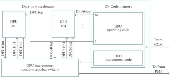
4.1. The Accelerator Architecture. The accelerator is composed
of a DF-Code memory, a custom crossbar switch (DFU
interconnect), and𝑛𝑑identical DFUs. Figure 4 refers to an
accelerator with𝑛𝑑 = 64 (64 represents a possible instance:
the actual number of DFUs, the associated DFU interconnect, and the DF-Code memory can vary according to the available on-chip resources).
DF-Code Memory. This memory stores the DPG
configura-tion (context) ready for execuconfigura-tion. The DFU interconnect code memory is a register bank that is dedicated to storing the
interconnect code (2 × 𝑛𝑑× ⌈log2𝑛𝑑⌉) bits. The DFU operating
code is a register bank that stores the DFU operating codes
(𝑛𝑑×10-bits). To simplify the transfer of information from the
management module to the accelerator there is a dedicated bus under the supervision of the management module.
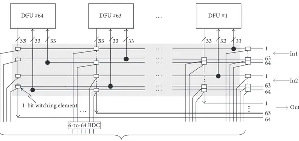
DFU Interconnect. The DFU interconnect, shown in Figure 6,
consists of a custom crossbar grid of wires connected by switching elements that allow for the connection of any DFU output to any DFU input, except itself, or to the parallel memory processor (PMP) in the management module (see next subsection). All switches along a column are controlled
by a⌈log2𝑛𝑑⌉-to-𝑛𝑑decoder. Across a row only a valid token
can exist because if two or more switches are enabled, they belong to some relational operation. But, in the hHLDS the operation is constituted by two or more actors in mutual exclusion; only the actor which satisfies the condition can generate the valid token. This feature is essential for imple-menting conditional and cyclic structures in conformance with the hHLDS model. When a decoder receives its own code, it enables the connection between the corresponding units or the PMP. The decoder control-signals come directly from the dedicated registers of the DFU interconnect code memory.
DFU #64 DFU operating code DFU interconnect code DFU64op DFU1op 64 1 DFU #1 DF U 1 O u t DF U 1 In 1 D FU1I n2 D FU64Ou t D FU64 In 1 DF U 6 4 In 2 DFU interconnect (custom crossbar switch)
DF-Code memory To/from PMP From CCM Data-flow accelerator .. . · · ·
Figure 4: The accelerator module.
Control Opera tin g co de r egi st er 10 1 1 1 2 1 1 1 1 1 5 33 32 32 33 33 Latch Latch Latch Enable In Enable Out LST Test Stream/pipe Const Comparison result V alidi ty V alidi ty Validity extended ALU
Figure 5: The DFU datapath.
Because the interconnect handles a large number of inputs and outputs, it is a crucial component of this architec-ture. Therefore, its sizing is chosen based on chip capabilities. Nevertheless, in a recent work [51], the authors have shown that it is possible to implement a crossbar interconnecting 128 tiles with an area cost of 6% of the total.
Data-Flow Functional Unit. A DFU (architecture shown in
Figure 5) implements any hHLDS actor, as defined in Sec-tion 2.1. It consumes two 33-bit (32-bit data and 1-bit validity) valid tokens (DFUIn1 and DFUIn2) and produces one 33-bit token (DFUOut). If the token is invalid, its validity bit is set
to0. A DFU is composed of a 32-bit fixed-point extended
ALU (arithmetic and comparison, multiplier, and divider) that implements the operator set and a 10-bit operating code register, which holds 5 bits for the operations and 5 bits
for the DFU context (constant token, token streaming, loop, pipelining, and conditional participation). The control unit ensures the right behavior of an extended ALU (eALU).
Control Unit and DFU Operation. When a valid input data
token reaches the DFU, the control unit catches its validity bit to match the partner operand. As soon as the match occurs, an enabling signal activates the input latches that acquire the values of two input data tokens (DFUIn1 and DFUIn2) so that the operation stored in the register can take place; we call this self-scheduling of the operator. After the (fixed) known time for the eALU operation, the control unit generates the validity bit for the output token, enables the output latch making available the result token, and resets the values of the two validity bits previously caught. The latches also isolate the internal DFU activities from the activity of other DFUs.
1-bit witching element DFU #1 DFU #63 DFU #64 1 1 64 63 63 63 64 64 1 In1 In2 Out 33 33 33 33 33 33 33 33 33
From the DF-Code 6-to-64 BDC .. . .. . .. . .. . .. . .. . .. . .. . · · · · · · · · · · · · · · · · · · · · · · · ·
Figure 6: DFU interconnection network.
To/from C o n text s ched u ler host SID SIN (CS C) To/from DFU interconnect To DFU-Code memory TERM Context management module Context configuration for context manager (CCM) Local memory processor (PMP) Parallel memory
for initial data and results Local memory
Figure 7: The management module.
Afterwards, a new firing process can start. The control unit also receives the five context bits for the eALU from the operating code register.
Operating Code Register. This register holds 5 bits. The first
bit, when set to 1, informs the control unit that the eALU will work in pipelining fashion because of token streaming. The second bit, when set, informs the control unit that the eALU is executing an LST operation. This is necessary because LST is the only operator fired by one token. In this case, since an eALU only executes binary operations, as soon as a single valid token is present at one DFU input, the control unit generates a dummy presence bit for the other input so that the LST operation can start. The third bit (test bit), when set, informs the control unit that the
eALU is executing a comparison operation. If the condition
is not satisfied, the control unit receives this information and resets token validity bit so that any other related DFU that follows it cannot fire. The last two bits—one for each input token—inform the control unit, when set, that the related data token will be reused. In this case the control unit sets the corresponding validity bit immediately after the reset signal.
4.2. The Context Management Module Architecture. It is
constituted by three fundamental submodules (Figure 7).
(i) Context Configuration Manager (CCM). Once the contexts
(i.e., the graph configuration) generated by the compiler are stored in the context configuration memory (a small local memory), they can be loaded dynamically into the accelerator as soon as the SNC signal (Send-Next-Configuration) is activated by the context scheduler submodule (see below).
(ii) Parallel Memory Processor (PMP). While the CCM takes
care of the program graph, this module takes care of the initial input data and collects the final output data that are processed by the accelerator. Therefore, once the scheduler enables the SID signal (Send-Initial-Data) in this submodule, the following actions are performed: (i) the initial data tokens are prepared to be transferred to the accelerator module; after having organized this transfer, (ii) the result data tokens are collected as soon as they are ready at the output buffer registers; when the computation ends, (iii) it sends a termination signal to the scheduler.
Front-end/translator Front-end Chiara Data/control flow to hHLDS converter Chiara language compiler Imperative Functional/data-flow languages languages 1 3 4 5 6 7 8 2
Mapper and scheduler
Processor description
Context #1
description descriptionContext #i Context #descriptionn
DFSC processor machine code D# (DPG) partitioner
D# language
Figure 8: The programming toolchain for the Data-Flow Soft-Core processor.
// Matrix multiplication𝐶(2, 2) = 𝐴(2, 2) × 𝐵(2, 2) // with𝑎11= 1, 𝑎12= 2, 𝑎21= 3, 𝑎22= 4
// with𝑏11= 5, 𝑏12= 6, 𝑏21= 7, 𝑏22= 8 // DP Dot Product
def DP =! + ∘ & ∗ ∘ trans
// the matrix multiplication function
&& DP∘ & distl ∘ distr ∘ [1, trans ∘ 2]: ⟨⟨⟨1, 2⟩, ⟨3, 4⟩⟩, ⟨⟨5, 6⟩, ⟨7, 8⟩⟩⟩ stop
Box 1: Chiara code for the matrix multiplication𝐶(2, 2) = 𝐴(2, 2) × 𝐵(2, 2).
(iii) Context Scheduler (CSC). Context scheduler (i)
imple-ments the scheduling policy (defined after the partitioning and mapping activities) for the contexts allocated on the CCM, (ii) sends enabling signals to the CCM (see above) and to the PMP (see above) parallel memory processor, and (iii) manages the interaction with the host.
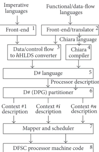
5. The Programming Toolchain
To turn programs into DPGs suitable for execution on the DFSC processor, we have developed some software tools, represented by blocks 4–8 of the toolchain of Figure 8. Blocks 1–3, under development, are dedicated to turning applications written in high level languages into graph contexts that the DFSC can execute. Here we only summarize the functionality of blocks 6–8, which is mostly beyond the scope of this paper. (1) Block 6 partitions a DPG in contexts according to the
number of DFUs inside the accelerator.
(2) Block 7 maps contexts onto the DFSC (or more DFSCs, if available) and creates the scheduling list for the context scheduler of the management module. (3) Block 8 generates the DFSC machine code.
To test the toolchain, we used Chiara language because it maps more directly onto the DFSC assembly language and has combinator operators which are compiled into suitable DFU connections at the level of DPG. An example of Chiara program code for the matrix multiplication is shown in Box 1, while Figure 9 shows D# code.
The program matrix multiplication has four steps, tied
by ∘ like 𝑓 ∘ 𝑔 functions, reading from right to left. Each
step is applied in turn, beginning with[1, trans ∘ 2], to the
result of its predecessor. The function dot product DP has three steps operating on conceptual units, as well, and no step is repeated. Moreover, this matrix multiplication program describes the essential operations of matrix multiplication without accounting for the process or obscuring parts of it
1 2 3 4 5 6 7 8 9 10 11 12 3 3 Out 6 6 Out 9 9 Out 12 12 Out %1 %2 1 %1 %2 4 %3 %4 7 %3 %4 10 %5 %7 2 %6 %8 5 %5 %7 8 %6 %8 11 MULT MULT ADD MULT MULT ADD MULT MULT ADD MULT MULT ADD Node # Left input Right input Func. Output (a) MULT MULT ADD out c11 2 3 1 MULT MULT ADD c22 11 12 10 MULT MULT ADD c12 5 6 4 MULT MULT ADD c21 8 9 7 %1%5 %2%7 %1%6 %2 %8 %3%5 %4%7 %3%6 %4%8
out out out
(b)
Figure 9: Matrix multiplication example: (a) DFSC assembly language and (b) graphical representation.
#include<math.h>
float fun (float x){return (x∗x+3∗x - 1.75);} int main(){
float xmd, a= -1.34, b=1.0, epserr=1e-6, fm;
do{ xmd=(a+b) / 2; fm=fun(xmd); if (fabs(fm) < epserr){ return 0;} else{if (fun(a)∗fm < 0) b=xmd; else a=xmd;}} while (fabs(fm)>= epserr); return 1;}
Box 2: Function root-finding with the bisection method: C code.
and yields the product of any pair ⟨𝑚, 𝑛⟩ of conformable
matrices.
Readers unfamiliar with functional programming lan-guages can make reference to Appendix B for more details on the Chiara language and the matrix multiplication code.
6. DFSC Evaluation
In a recent paper [1], Flynn et al. argued that unconventional models of computation, for example, computation systems developed by Maxeler Technologies [7], when dealing with highly data-intensive workloads, show a better speedup than computers listed in the Top 500, but these systems do not appear in the Top 500 list. Also, their perspective about the performance is that metric should become multidimensional, measuring more than just FLOPS, for example, performance per watt, performance per cubic foot, or performance per monetary unit. However, the issue to evaluate radically different models of computation, such as data-flow, remains yet to be addressed. The reason is because, for custom data-flow systems, the current performance metrics do not take into account parameters, such as less power consumption, pin throughput, and local memory size/bandwidth.
Our DFSC processor falls into the asynchronous data-flow category. We recall that the DFSC processor is totally asynchronous, does not store partial results during the accel-erator run, and employs an ad hoc memory in the context management, which acts differently from a cache, since it manages the execution of contexts in the accelerator. Here we evaluate the proposed architecture for two cases: cyclic and acyclic as reference examples. The system can change the
program without uploading a new bit-stream (differently from classical FPGA accelerators). To show the poten-tial of the DFSC, we used two simple but quite differ-ent algorithms—the bisection method, for finding a func-tion roots, and the matrix multiplicafunc-tion—cyclic (data-dependent), the former, and acyclic, the latter.
6.1. Bisection Method Root-Finding. The bisection method for
finding roots of a function represents an example of data-dependent iteration, where the cyclic flow of data is the only
algorithm requirement. Given a function𝑓(𝑥), continuous on
a closed interval[𝑎, 𝑏], such that 𝑓(𝑎) × 𝑓(𝑏) < 0, then the
function𝑓(𝑥) has at least a root (or zero) in the interval [𝑎, 𝑏].
The method calls for a repeated halving of subintervals of [𝑎, 𝑏] containing the root. The root always converges, though more slowly than others.
For this algorithm, we only made a qualitative evaluation between the assembly codes for an x86 processor (the C program in Box 2) and D# code for the DFSC. The main reason is that a comparison time could not be fair due to the different execution times of a cycle for both x86 technologies (from Intel Pentium Dual CPU at 2 GHz to Core(TM)-i7 at
2.76 GHz) and the DFSC technology (180𝜇m and 32 ns for
the execution time of a DFU). In fact, the run of the algorithm code in Box 2 for finding the root requires 22 cycles, while the execution times for the Dual CPU, the Core(TM)-i7, and
the DFSC are 29 ms, 27 ns, and 8.5𝜇s, respectively. However,
to give a sense of what happens with our processor, we report some qualitative evaluation. Observing the two low-level codes shown in Box 3 and Figure 10, a first interesting point is the simplicity and intelligibility of each D# code
.file "bisection2.c" fxch %st(3) xorl %eax, %eax .section fxch %st(2) ret .text.unlikely,"ax",@progbits fxch %st(1) .L10: .LCOLDB3: .L3: fstp %st(0) .text fld %st(0) fstp %st(0) .LHOTB3: fmul %st(1), %st fstp %st(0) .p2align 4,, 15 flds .LC0 fstp %st(0)
.globl fun fld %st(2) movl $1, %eax
.type fun, @function fmul %st(1), %st ret
fun: faddp %st, %st(2) .cfi endproc
.LFB33: flds .LC1 .LFE34:
.cfi startproc fsubr %st, %st(2) .size main, .-main
flds 4(%esp) fxch %st(7) .section .text.unlikely
fld %st(0) fmulp %st, %st(2) .LCOLDE13:
fmul %st(1), %st fldz .section .text.startup
fxch %st(1) fucomip %st(2), %st .LHOTE13:
fmuls .LC0 fstp %st(1) .section .rodata.cst4,"aM",@progbits,4
faddp %st, %st(1) fxch %st(1) .align 4
fsubs .LC1 fcmovbe %st(3), %st .LC0:
ret fxch %st(2) .long 1077936128
.cfi endproc fcmovnbe %st(3), %st .align 4
.LFE33: fstp %st(3) .LC1:
.size fun, .-fun fldl .LC12 .long 1071644672
.section .text.unlikely fxch %st(4) .align 4
.LCOLDE3: fucomip %st(4), %st .LC4:
.text fstp %st(3) .long 3222194776
.LHOTE3: jb .L10 .align 4
.section .text.unlikely fld %st(0) .LC5:
.LCOLDB13: fadd %st(2), %st .long 1074711128
.section fmuls .LC9 .align 4
.text.startup, "ax",@progbits fld %st(0) .LC6:
.LHOTB13: fmul %st(1), %st .long 3190690940
.p2align 4,, 15 fxch %st(4) .align 4
.globl main fmul %st(1), %st .LC8:
.type main, @function faddp %st, %st(4) .long 3215688991
main: fxch %st(3) .align 4
.LFB34: fsubp %st, %st(4) .LC9:
.cfi startproc fld %st(3) .long 1056964608
flds .LC4 fabs .section .rodata.cst8,"aM",@progbits,8
flds .LC5 fldl .LC12 .align 8
flds .LC6 fucomip %st(1), %st .LC12:
fld1 jbe .L11 .long 1073741824
flds .LC8 fstp %st(0) .long 1065646817
jmp .L3 fstp %st(0) .ident "GCC: (GNU) 5.3.1 20151207
.p2align 4,, 10 fstp %st(0) (Red Hat 5.3.1-2)"
.p2align 3 fstp %st(0) .section .note.GNU-stack,"",@progbits
.L11: fstp %st(0)
Box 3: Function root-finding with the bisection method: assembly code for a Pentium Dual CPU.
line (Section 2) compared with the x86 code. Another point is that we can easily evaluate the time required to execute a context without running it. Then, loaded the D# code, the accelerator works it out asynchronously while partial results flow between DFUs until the final result is not ready. Because the computation gets along without storing any partial data, another important fact of this organization is that both temporary data and instructions are eliminated as traffic over the memory access busses. Consequently, avoiding the communication traffic over the accelerator, the
DFSC processor provides the advantage to naturally augment speedup and reduce latency drastically for a given technology.
6.2. Matrix Multiplication. Matrix multiplication 𝐴(𝑛, 𝑛) ×
𝐵(𝑛, 𝑛) is an example of an intrinsically acyclic algorithm and constitutes the kernel for many linear algebra-based applica-tions. Despite its algorithmic simplicity, it is computationally
complex and memory intensive,𝑂(𝑛3) for two matrices 𝑛 × 𝑛.
Moreover, its algorithm perfectly matches an interconnection mode configurable architecture since each dot product forms
Actor # 1 2 3 4 5 6 7 8 9 10 11 12 13 14 15 16 17 18 19 20 21 22 23 24 25 26 27 28 LST LST ADD DIV MUL MUL MUL MUL ADD ADD SUB SUB MUL LT EQ GT ADD ADD ADD ADD ADD ADD SUB GEQ LT ADD ADD ADD Left input 26 27 1 3 1 1 4 4 5 7 9 10 11 13 13 13 1 14 4 15 2 16 17-19-21 23 23 17-19-21 27 25 Right input 2 2% 1 3% 4 3% 6 8 1.75% 1.75% 12 0% 0% 0% 14 4 15 4 16 1 18-20-22 24 0.01% 0.01% 18-20-22 4 3-5-6-17 3-21 4 7-8-18-19-20-22-28 9 9 10 10 11 12 13 13 14-15-16 17-18 19-20 21-22 23-26 23-27 23-26 23-27 23-26 23-27 24-25 26-27 28 1 2 Out Func. Output %−1.34 %1 (a) D# code 4 / 3 + 2 LST 1 LST + 13∗ 17 + 18 + 14 > 19 + 20 + 15 = 6 ∗ 9 11 − 5 ∗ 8 ∗ + 10 12 − 7 ∗ 21 + 22 + 16 > 26 + 27 + 24 23 − 28 + 25 < Out −1.34 1.00 0.01 0.00 0.00 3.00 1.75 2.00 1.75 3.00 0.00 0.01 Epserr Epserr ≤ (b) DPG representation
Figure 10: Function root-finding with the bisection method.
a reversed binary-tree graph. More in general, the DFSC processor is capable of executing any program represented by a DPG; however, for the sake of a more effective illustration, we prefer to focus on this simple example in this paper. For the matrix multiplication we compared three different execution architectures with the DFSC processor: the SIMD extension of an x86 architecture (shortly SIMD-x86), the tile-based FPGA architecture (shortly FPGA-tile-based) proposed by Campbell and Khatri [52], and the Cyclops-64 chip [53].
6.2.1. The Matrix Multiplication Evaluation Model. Given two
matrices𝐴(𝑁, 𝑀) and 𝐵(𝑀, 𝑃), where 𝑎𝑖,𝑗with𝑖 = 1, 2, . . . , 𝑁
and 𝑗 = 1, 2, . . . , 𝑀 is an element of 𝐴 and 𝑏𝑗,𝑘 with𝑗 =
1, 2, . . . , 𝑀 and 𝑘 = 1, 2, . . . , 𝑃 is an element of 𝐵, the product
𝐶(𝑁, 𝑃) = 𝐴(𝑁, 𝑀) × 𝐵(𝑀, 𝑃) can be expressed with 𝑛dp =
𝑁 × 𝑃 independent dot products (a𝑖⋅ b𝑘) of the 𝑁 row vectors
of𝐴 and 𝑃 column vectors of 𝐵 whose dimensions are 𝑀:
a𝑖= {𝑎𝑖1, 𝑎𝑖2, . . . , 𝑎𝑖𝑀} 𝑖 = 1, 2, . . . , 𝑁,
b𝑘= {𝑏1𝑘, 𝑏2𝑘, . . . , 𝑏𝑀𝑘} 𝑘 = 1, 2, . . . , 𝑃.
(5)
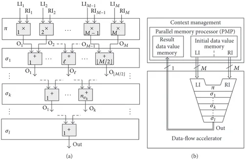
Figure 11(a) shows the DPG of the dot product in D# graphical representation where LI, RI, and O represent the left and right inputs, and the output sets of tokens, respectively, as defined in D# language. It shapes a reversed binary-tree graph
with2𝑀 − 1 actors; 𝑀 are organized in one level 𝜋 of parallel
Out LI1 LI2 LIM−1 LIM RI1 RI2 RIM−1 RIM 𝜋 𝜎1 𝜎k 𝜎l .. . .. . .. . .. . · · · · · · · · · · 1 1 2 M − 1 M + + + + + + 1 1 ⌊M/2⌋ O⌊M/2⌋ n𝜎𝑘 × × × × O1 O1 O1 Ok O2 OM−1 OM O (a) Data-flow accelerator memory Initial data value Parallel memory processor (PMP)
Context management RI Result data value memory Out LI LI 1 M M RI 𝜋 𝜎1 𝜎k 𝜎l .. . .. . (b)
Figure 11: Dot product: (a) the DPG and (b) the generalized DFSC.
of𝜎 additions, where each level 𝑙𝑘 ∈ [1 ≤ 𝑘 ≤ 𝑙] broadens a
number𝑛𝜎𝑘of parallel additions:
𝑛𝜎𝑘= [ [ [ [ 𝑀 − ∑𝑘−1𝑗=1𝑛𝜎𝑗 2 ] ] ] ] . (6)
Figure 11(b) shows the generalized DFSC (shortly gDFSC) processor (in this context, the term generalized DFSC pro-cessor refers to an abstract DFSC propro-cessor architecture whose resources are always sufficient to compute any one dot product) with the related context management and data-flow accelerator. Like actors in the DPG, DFUs in the accelerator are organized in the same number of levels (stages); in the context management, the parallel memory processor (PMP) is organized in two stages—one to send the initial values and one to receive the final value. The latency parameters, which characterize a computation to the inside of the gDFSC processor, can be defined as follows.
Definitions. Let{𝜏tr𝑖 : 1 ≤ 𝑖 ≤ 𝑀} be the set of latencies
required to transfer the corresponding single tokens between
the PMP and accelerator registers; let{𝜏𝑚𝑖 : 1 ≤ 𝑖 ≤ 𝑀} be
the set of latencies that each DFU requires for a multiplication
operation; and let{𝜏𝑎𝑖 : 1 ≤ 𝑖 ≤ 𝑀 − 1} be the set of latencies
that each DFU requires for an addition operation. The latency for the token transfer between the PMP and the accelerator is
defined as𝜏tr = max𝑖𝜏tr𝑖, the latency for the multiplication is
defined as𝜏𝑚 = max𝑖𝜏𝑚𝑖, and the latency for the addition is
defined as𝜏𝑎= max𝑖𝜏𝑎𝑖.
It follows that, for a given𝑀, the gDFSC computes the
dot product in a time𝑡dp:
𝑡dp(𝑀) = 𝜏tr+ 𝜏𝑚+ 𝑙 (𝑀) × 𝜏𝑎. (7)
We point out that, when2𝑟< 𝑀 ≤ 2𝑟+1∀𝑟 ∈ Z+,𝑡dpremains
constant although the number of operations changes. This
1 50 100 150 200 250 300 350 400 450 500 M
t∗dp
Figure 12: Computation time for the dot product𝑡∗dp(𝑀).
occurs because, in the DPG, the number of levels does not
change. Moreover, the relation between𝑡dp(𝑀) and 𝑀 can be
expressed with the following step function:
𝑡∗dp(𝑀) =
𝑛
∑
𝑖=1
𝑡𝑖dp(𝑀) , (8)
where𝑡𝑖dpis the dot product time when𝑀 varies in the 𝑖th
domain(2𝑟𝑖, 2(𝑟+1)𝑖].
Table 2 summarizes the features of the generalized proces-sor configured to execute a dot product. Figure 12 draws the
computation time𝑡∗dp(𝑀) for different values of 𝑀, whereas
gDFSC throughput rate TP is
TP= 1
𝑡∗
dp(𝑀)
, (9)
while gDFSC computes the matrix product in a time𝑇mp(𝑀):
𝑇mp(𝑀) = 𝑛dp× 𝑡dp(𝑀) with 𝑛dp= 𝑁 × 𝑃. (10)
To reduce𝑇mp, it is possible to apply the linear pipelining
technique to the dot product computation because its DPG is naturally organized to support such a technique. In this case,
Table 2: Characteristics of the𝑔DFSC processor for a dot product.
Level DAC number Operation type time Parallelism degree (spatial)
1 𝑀 multiply 𝜏𝑚 𝑀 2 ⌊𝑀/2⌋ add 𝜏𝑎 ⌊𝑀/2⌋ ... ... ... ... ... 𝑖 ⌊(𝑀 − ∑𝑖−1𝑗=1𝑛𝜎𝑗)/2⌋ add 𝜏𝑎 ⌊(𝑀 − ∑ 𝑖−1 𝑗=1𝑛𝜎𝑗)/2⌋ ... ... ... ... ... 𝐿 = 1 + 𝑙 1 add 𝜏𝑎 1 Computing time𝑡dp= 𝜏𝑚+ 𝑙 × 𝜏𝑎
the hHLDS firing rules can guarantee the determinate com-putation during the asynchronous execution. It is possible to
further decrease𝑇mpusing pipelined DFUs as well. Anyway,
here we are only interested in showing gDFSC adaptability to simultaneously support different forms of parallelism and speed up an algorithm execution.
The dot product execution is composed of three
sequen-tial tasks—tsktr for the token transfer between PMP and
accelerator, tsk𝑚for the token multiplication, and tsk𝑎for the
token addition, whereas in the pipelined mode, the pipeline
period𝜏𝑝is𝜏𝑝= max (𝜏tr, 𝜏𝑚, 𝜏𝑎) and the pipeline throughput
rate TP𝑃is
TP𝑃= 1
𝜏𝑝. (11)
When𝑀 ̸= 2𝑖, the pipelined execution needs interstage
latches to correctly compute the dot product. In this case, the interstage latches are turned into adequate delays inside the initial data value memory of PMP. After that, the computation advances asynchronously.
Speedup. To fill all of the pipeline stages and produce the first
result, the gDFSC takes a time𝑡dp(𝑀). After that, each dot
product result comes out after every𝜏𝑝. Hence the total time
𝑇𝑃
mp, to process all of𝑛dpdot products in the2 + 𝑙(𝑀) stages
pipeline, is
𝑇mp𝑃 (𝑀) = [(1 + 𝑙 (𝑀)) + 𝑛dp] × 𝜏𝑝, (12)
and the speedup SP(𝑀) is given by
SP(𝑀) = lim𝑛 dp→∞ 𝑇mp(𝑀) 𝑇𝑃 mp(𝑀) = 2 + 𝑙 (𝑀) . (13)
Anyway, for 𝑛dp ≫ 2 + 𝑙(𝑀) (≫ refers to the wanted
precision), we can assume SP(𝑀) = 2 + 𝑙(𝑀). Besides, the
number of flops𝑛flopin pipelined mode is given by
𝑛flop(𝑀) =
2𝑀 − 1
𝜏𝑝 . (14)
6.3. DFSC Characterization. To characterize the DFSC,
we used a custom board demonstrator with two Altera APEX20K1500E devices with 51840 Logic Elements (LEs)
and 442368 RAM bits (without reducing available logic) inside the 216 Embedded System Blocks (ESBs) that allow the implementation of multiple memory functions (dual-port RAM, FIFO, ROM, etc.). The two devices are connected via six 132-bit buses to exploit the 808 tristate I/O user pins, and on the board is a pipelined SRAM memory to store contexts and tokens in case their number exceeds the local memory capacities of the management module. Finally, the board uses a PCI/interface to connect to the host. Our
implemented instance consists of𝑛𝑑 = 64 DFUs (Section 4)
and executes operations on 32-fixed-point operands. Device-1 is dedicated to the implementation of the context module plus 32 DFUs. Device-2 is dedicated to the implementation of the accelerator module with 32 DFUs and the custom crossbar interconnect (due to the interconnect area penalty). Table 3 reports the resources required for Device-1 and Device-2 implementations. Please note that in a previous paper [17] we evaluated the latencies of a DFU, register-to-register, and the context switch which are 32 ns, 7 ns (device-to-device registers) and 4 ns (internal registers), and 32 ns, respectively.
The matrix multiplication 𝐶(𝑛, 𝑛) = 𝐴(𝑛, 𝑛) × 𝐵(𝑛, 𝑛) in
D# consists of 𝑛2 independent inner products (IPs) whose
DPGs are organized in identically reversed binary-trees, each
consisting of𝑛 multiplications and 𝑛 − 1 additions sequenced
in log2+1 levels. Thanks to its shape, the inner product DPG is
well suited for a naturally pipelined execution, thus allowing for speedup of the matrix multiplication computation.
Here we evaluate the product of matrices for𝐴 and 𝐵 in
pipelining. For the test we used matrix dimensions𝑛 = 32
and𝑛 = 64, respectively, with all matrix elements residing in
the local data memory of the context management module.
For𝑛 = 32 the inner product (IP) DPG is wholly mapped
onto the DFSC processor, by means of 63 out of 64 DFUs available (Figure 13(a)). We point out that 64 is the biggest tile size that can be considered because the PMP does not
need any optimization of load and store activities. For𝑛 = 64
we split the DPG into two sub-DPGs as we did for𝑛 = 32.
Then, we execute the two inner products IP= 𝑛𝑎
𝑖/2×𝑛𝑏𝑗/2 and
IP = 𝑛𝑎
𝑖/2× 𝑛𝑏𝑗/2 and use the DFU #64 to add the two results
as shown in Figure 13(b). We would like to point out that this decomposition does not hinder the execution (throughput) of an inner product IP when pipelining occurs because the DPG in Figure 13(b) behaves as if all the required DFUs were in the DFSC but doubles the number of IPs to execute.
Table 3: DFSC: APEX 20K-1500E FPGA resources (total LEs = 51840; total RAM bits = 442368). Context management (Device-1)
I/O Token buffers 32 DFUs CCM PMP Scheduler
LEs 0 11766 187 384 215
RAM bits 6336 0 8448 406912 0
Accelerator (Device-2)
I/O Token buffers 32 DFUs Switch interconnect DF-Code memory
LEs 0 11766 36365 386 RAM bits 6336 0 0 1408 Token_I 32 MUL T Token_O Context C u st o m cr oss ba r in te rc on n ec t 16 AD D 8 AD D 4 AD D 2 AD D 1 AD D OpCodes SID TERM SNC CCM PMP Token_I1 Token_I2
Altera APEX20K1500E Altera APEX20K1500E
Switching element Shifter register NetCode L1 L2 ADD (a) (b) Result data local memory
Initial data local memory
Context local memory DF-Code memory
C o n text s ched u ler T o/f ro m host
Figure 13: DPG for the inner products (a)𝑛 = 32 and (b) 𝑛 = 64.
6.4. SIMD-x86 and FPGA-Tile-Based versus DFSC. To make
a fair DFSC comparison between the SIMD-x86 and the FPGA-tile-based [52], which act at different clock rates (2 GHz for the SIMD-x86 and 400 MHz for the FPGA-tile-based) and are based on different state-of-the-art technolo-gies, we measured, for the matrix multiplication, the perfor-mance in terms of cycles per instructions rather than in terms of GFLOPs because, in [52], authors used this parameter to evaluate their FPGA-tile-based processing element. To avoid the large time penalty incurring each time to fetch an element from x86 L2 cache and to compare our results with those reported for the FPGA-tile-based, we used matrices of size 𝑛 = 32 and 𝑛 = 64, respectively. For the DFSC we determined the number of stages and the stage clock rate involved in an IP computation in pipelining as well.
DFSC Execution. The parallel execution of the 32
multiplica-tions on the management module requires the move from the
PMP local memory to the 32 DFU of2 × 32 = 64 tokens (In1
and In2). Since the token is 33 bits, the total number of bits
to be moved to the 32 DFUs is33 × 64 = 2112. By exploiting
the internal FPGA interconnect, we can transfer2 × 4 tokens
(264+264 bits) at a time. In total this takes 8x internal
register-to-register transfers and has a latency equal to8 × 4 = 32 ns,
while the multiplication needs 30 ns. Transferring32 × 33-bit
tokens of the product from the management module to the
accelerator requires 4x external register-to-register transfers
and latency of4×7 = 28 ns, whereas inside the accelerator the
transfer of the input buffers to the 32 DFUs in the first level
requires latency of4 × 4 = 16 ns.
When𝑛 = 32, we need 30 ns for each additional level
(log2(32) + 1 = 6 total levels) and 11 ns to transfer 𝑐𝑖𝑗back to
the management module. Therefore, the pipeline requires a
number of stages𝑛𝑠 = 11 to fill it with a stage latency 𝜏𝑝 =
32 ns (clock rate 31,2 MHz). The total number of cycles 𝑛𝑐
required for the matrix multiplication is𝑛𝑐= 322+11 = 1035.
When 𝑛 = 64, the DFSC processor requires the same
latencies as with 𝑛 = 32 up to the DFU #63. Then the
DFU #64, through the two cascaded latches L1 and L2 in
Figure 13(b) produces𝑐𝑖𝑗. In this case we add the first latch
latency (4 ns) to the DFU #63 latency while the second latch latency is added to the DFU #64 latency. Consequently, we
have𝜏𝑝 = 34 ns (clock rate 29,4 MHz), 𝑛𝑙= log2(64) + 1 = 7
number of levels in the accelerator, and𝑛𝑠 = 13, while the
number of IPs doubles. The total number of cycles𝑛𝑐required
for the matrix multiplication, in this case, is𝑛𝑐= 2×642+13 =
8205.
SIMD-x86 Execution. Multimedia Extension (MMX)
tech-nology provides acceleration through SIMD parallelism providing SIMD multiplication and addition instructions where two 32-bit integer values are operated on at once. To
Table 4: SIMD-x86 and FPGA-tile-based versus DFSC. 𝑛 SIMD-x86 cycles FPGA-tile-based
cycles
DFSC cycles
32 16131 2081 1035
64 130098 16417 8205
determine the number of clock cycles, we used the related built-in hardware performance counter.
FPGA-Tile-Based Execution. The FPGA-tile-based considered
[52] implements the matrix multiplication algorithm in a Xilinx Virtex-4 XC4VSX55-12 FPGA (which is similar to the one we used for the DFSC) and consists of an array of PEs as in a CGRA. Each PE operates at 400 MHz independently of the other PEs in the array and the operating frequency of the PE array is independent of matrix dimension. The PE
structure consists of one input each from matrices 𝐴 and
𝐵, a multiplier accumulator (MAC), and a result FIFO. The
inputs from matrices𝐴 and 𝐵, one word each per clock cycle,
are implemented using dedicated routes from the BlockRam memory associated with the multiplier, thus eliminating the routing and resource delay penalty.
Each matrix is partitioned into𝑚 BlockRam banks. Each
of the banks dedicated to𝐴 stores 𝑘 = (𝑛/𝑚) words of each
column in𝐴, for every row of 𝐴. Each of the banks dedicated
to 𝐵 stores 𝑘 = (𝑛/𝑚) words of each row in 𝐵, for every
column of𝐵, requiring a number of cycles of 2081 for 𝑛 = 32
and 16417 for𝑛 = 64.
Comparison Results. Table 4 shows the comparison results
in terms of number of cycles and execution time for matrix
multiplications with𝑛 = 32 and 𝑛 = 64, respectively.
As we can observe, regarding the number of cycles the DFCS processor performs better than a SIMD-x86 (roughly
15 times for 𝑛 = 32 and 8 times for 𝑛 = 64) and the
FPGA-tile-based (roughly 2 times for𝑛 = 32), but regarding
the execution time it performs worse than them. However, if we consider that the technology of current FPGAs can allow DFUs to operate at 400 MHz, the Data-Flow Soft-Core becomes quite interesting and competitive to a dedicated out-of-order processor or dedicated solutions on FPGAs.
6.5. Cyclops-64 versus DFSC. For this comparison, we
inter-polated the data assuming an FPGA with 300 floating-point DFUs and a clock rate at 500 MHz. From the other part, the multithreading many-core platform IBM Cyclops-64 [53] consists of 160 cores on a single chip. In particular, each Cyclops-64 processor (C64 for short) consists of an 80 cores with two Thread Units (TU) per core, a port to the on-chip interconnect, external DRAM, and a small amount of external interface logic. The TU is a simple 64-bit, single issue, in-order RISC processor operating at a moderate clock rate (500 MHz). A software thread maps directly onto a TU and the execution is nonpreemptive; that is, the microkernel will not interrupt the execution of a user application unless an exception occurs (no context switch). Each thread controls a region of the scratchpad memory, allocated at boot time.
Table 5: Cyclops-64 versus simulated 300 DFU DFSC-based pro-cessor.
Machine characteristics
Cyclops-64 node DFSC
Number of cores 160 (classical) 300 (DFUs) Memory hierarchy
level 3 1
Architecture model Hybrid Pure data-flow
Program execution
model Tiny-Thread (TNT)
Interconnected DPGs
Performance Simulated Interpolated
70.0 GFlops1 123 GFlops2 0.43 GFlops 0.41 Gflops
1Input data on a chip.2Included transfer time from PMP to accelerator.
Moreover, there is no hardware virtual memory manager so the three-level memory hierarchy is visible to the pro-grammer. The comparison with the Cyclops-64 is interesting in this context because it uses a data-flow-based execution model. For the C64 platform we refer to the run with a FAST Simulator [54] of a test based on a highly optimized dense matrix multiplication using both on-chip and off-chip memory. Both static and dynamic scheduling strategies were implemented [55–57]. We optimized the code so that the DFSC execution could take place in pipeline. In our case, we first performed the multiplications in parallel and then we
performed the additions in log2(𝑛) stages.
This evaluation compares the GFLOPS-per-core of the two architectures when the two processors execute a matrix
multiply300 × 300. The result of this comparison is reported
in Table 5.
7. CGRA versus DFSC
In this section we discuss and compare some CGRA architec-ture with the DFSC processor MorphoSys System [46] having a MIPS-like Tiny RISC processor with extended instruction set that executes sequential tasks, a mesh-connected 8 by 8 reconfigurable array (RA), a frame buffer for intermediate data, context memory, and DMA controller. The RA is divided into four quadrants of 4 by 4 16-bit RCs each, featuring ALU, multiplier, shifter, register file, and a 32-bit context register for storing the configuration word. The interconnect network uses 2D mesh and a hierarchical bus to span the whole array. Tiny RISC extra DMA instructions initiate data transfers between the main memory and the “frame buffer” internal data memory for blocks of inter-mediate results, 128 by 16 bytes in total. Programming frameworks for RAs are highly dependent on structure and granularity and differ by language level. For MorphoSys, it is assembler level. It is supported by a SUIF-based compiler for host and development tools for RA. Configuration code is generated via a graphical user interface or manually from an assembler level source also usable to simulate the architecture from VHDL. In contrast, the DFSC processor
exhibits MIMD functionality, its interconnect is crossbar-like so that intermediate results are asynchronously passed directly from a data-flow functional unit to another avoiding so to store partial results, and its context switching is managed by the Context Configuration Manager (CCM) according to the operations to be executed. As an example, in pipelined operations involving data-flow functional units as pipeline stages, the context does not change while a new input data stream arrives.
ADRES [58], designed for Software Defined Radio
appli-cations, is a reconfigurable processor with tightly coupled VLIW processor. Each reconfigurable cell has mainly a functional unit (FU) and a register file that contains a 32-bit ALU which can be configured to implement one of sev-eral functions including addition, multiplication, and logic functions, with two small register files. It utilizes MorphoSys communication mechanism and resolves resource conflict at compile time using modulo scheduling. If the application requires functions which match the capabilities of the ALU, these functions can be very efficiently implemented in this architecture. Applications, written in ANSI-C, are trans-formed into an optimized binary file. However, exploiting instruction level parallelism (ILP) out of ADRES architecture can cause hardware and software (compiler) inefficiency because of the heavily ported global register file and multi-degree point-to-point connections. In contrast, in the DFSC, since the accelerator does not store intermediate data during an execution, the execution of data-dependent loops (cycles) happens asynchronously with the only control of the data-flow functional unit (DFU) firing rule implementation.
KressArray [59] is a 2D mesh of rDPUs (reconfigurable
datapath units) physically connected through local nearest neighbor (NN) link-spots and global interconnection. The KressArray is a supersystolic array. Its interconnect fabric distinguishes 3 physical levels: multiple unidirectional and/or bidirectional NN link-spots, full length or segmented column or row back buses, and a single global bus reaching all rDPUs (also for configuration). Each rDPU can serve for routing only, as an operator, or an operator with extra routing paths. With the new Xplorer environment [60] rDPUs also support other operators (branching, while and do-while loops, etc.). Differently, the DFSC processor supports asynchronous com-putations without the need for global synchronization, uses a crossbar-like interconnect to link the DFUs, and allows on-the-fly context switching.
8. Conclusions
This paper presented the Data-Flow Soft-Core architecture. We evaluated this new concept of soft-core by using two simple test cases based on the bisection method and matrix multiply programs. The results that we obtained show a sizable reduction of the number of microoperations, typical in conventional core, and a competitive advantage both against reduced data-flow engines like the classical out-of-order processors and dedicated FPGAs and against the data-flow-based Cyclops-64. We believe that this processor needs further development but represents a first step toward a more flexible execution of generic programs on a scalable
input (a, b = 1, c) repeat if a > 1 then a fl a \ 2 else a fl a ∗ 5 b fl b ∗ 3; until b = c; d fl a; output (d)
Listing 1: A sample program.
reconfigurable platform. The Data-Flow Soft-Core introduces a new level of programmability that enhances the usability of FPGA platforms through the use of data-flow instructions rather than pretending to convert control-flow instructions, like what happens with the bisection method and matrix multiplication algorithms.
Appendix
A. Classical Model versus
hHLDS
To better understand the difference between the classical model and hHLDS, let us consider the sample program
pseu-docode in Listing 1, where𝑎, 𝑏, and 𝑐 are the input and 𝑑 is
the output data. Figure 14 shows the equivalent well-behaved DPGs with the classical model and hHLDS, respectively. For each DFG, the part inside the grey rectangle computes something, while the remaining part checks the end of the
computation and outputs𝑑. The DPG in Figure 14(a) has five
types of actors:𝛼 for merge, 𝛽 for switch, 𝛾 for gate, 𝛿 for
decider, and𝜖 for operator. Each of them has heterogeneous
I/O conditions, link-spots (places to hold tokens), and tokens; data link-spots hold data tokens and control link-spots hold control tokens. As can be observed, this representation presents some issues. First, to comprehend how the DPG works, we have to follow the flow of two types of tokens along a graph where there are actors with different numbers of input and output link-spots that can consume and produce them.
Then, the initial behavior of the actors𝛼, 𝛽, and 𝛾 depends on
their position in the DPG rather than program input values. The initial control tokens F and T (red dots in Figure 14(a)) for
the𝛼 and 𝛽 actors are automatically present on their control
arcs but have different values (false and true, resp.) although they share the same link-spot. As this condition cannot be true, it can be only managed via software because the classical DPG represents the schema of what we want to do, not what we really do. However, these control values, even if they might be deduced, are not a program input but a programmer’s trick to allow the computation to start correctly. Besides, not all functions associated with actors are defined in the same domain and assume a value in the same codomain. For example, if R is a subset of real numbers, B is the set of boolean values, and W is the set R × 𝐵, we note that the