F. Giordano(4)(5), M. Ionica(1), F. Licciulli(4)(5), S. Loporchio(4)(5), F. R. Pantaleo(4)(5), R. Paoletti(7)(8), A. Rugliancich(7)(8), L. Tosti(1)(3), V. Vagelli(1)(3) and L. di Venere(4) for the CTA Consortium
(1) INFN, Sezione di Perugia - Perugia, Italy (2) INFN, Sezione di Napoli - Napoli, Italy
(3) Universit`a degli Studi di Perugia - Perugia, Italy (4) INFN, Sezione di Bari - Bari, Italy
(5) Dipartimento Interateneo di Fisica dell’Universit`a e del Politecnico di Bari - Bari, Italy (6) Universit`a degli Studi di Napoli - Napoli, Italy
(7) Universit`a di Siena - Siena, Italy (8) INFN, Sezione di Pisa - Pisa, Italy
received 8 June 2020
Summary. — Silicon photomultipliers (SiPM) are a typology of solid-state sensors
that in recent years are replacing the established photomultiplier tube technology in a variety of uses. This kind of sensors find high demand in experiments carried out at very low light intensity (in the order of single photon detection) and also where high temporal precision (of the order of ns) and a reduced geometric encumbrance is required. The Bruno Kessler Foundation (FBK) has developed the near ultra violet high density low cross-talk (NUV-HD Low-CT) sensor optimized for the detection of photons in the ultraviolet spectrum jointly with a minimization of the optical cross-talk between adjacent microcells. These sensors are particularly suitable for equipping the imaging air cherenkov telescopes as intended for the CTA observatory. Optical modules consisting of 16 SiPMs (each one of 6× 6 mm2) were assembled in INFN laboratories to be integrated into the focal plane of the medium-sized telescope prototype with a Schwarzschild-Couder double-mirror optic (SCT). This report will describe the test procedures to verify the performance of these 6×6 mm2 sensors. Furthermore the assembly procedures developed to integrate the sensors on the detection modules and equip the focal plane chamber of the SCT prototype telescope (currently operational and under testing at the Fred Lawrence Whipple Observatory, Arizona) will also be presented.
Fig. 1. – Left: measure of PDE for different values of wavelength at fixed bias tension of +6 V over the breakdown voltage (about 26.3 V). Right: stability of the value of the PDE for different overvoltage values. This measurement was taken at 400 nm.
The Cherenkov Telescope Array (CTA, [1]) will be the largest ground-based gamma ray observatory for very high-energy gamma rays. CTA will be installed in two sites (one in each hemisphere). It will be equipped with more than 100 telescopes in three different configurations: Large-, Medium- and Small-Sized Telescopes (LST, MST and SST) and will be fully operational by 2025.
Istituto Nazionale di Fisica Nucleare (INFN) is involved with Fondazione Bruno Kessler (FBK) in the development of silicon photomultiplier sensors (SiPM) sensitive to near UV wavelengths, NUV-HD3, for the CTA telescopes to equip part of the MST telescopes with focal planes made of SiPM.
The sensors were developed to achieve the maximum photon detection efficiency (PDE) around the range of wavelengths at the maximum of the Cherenkov light emission (about 320–350 nm), as shown in fig. 1 (left).
The PDE value depends on the value of the overvoltage bias applied to the sensors
Fig. 2. – Left: INFN module (in orange) during the bonding procedure. Right: magnification of two of the bonding pads and wire bonds after the assembly procedure.
Fig. 3. – Left: example of the log-derivative fit on one SiPM. Right: histogram of the measured value of the breakdown voltages of the entire population of the tested sensors (50 modules, 800 SiPM). The gray scale represent the 36 modules chosen to equip the SCT focal plane. The difference shown by the Gaussian fit it is due to the different wafer used.
(the difference of bias voltage V and the breakdown voltage Vbr). The PDE reaches a
plateau above overvoltages of +5 V as shown in fig. 1 (right) where the PDE for 400 nm incident light is shown.
These SiPMs have been integrated in basic optical units made of 16 pixels (each one with 6× 6 mm2area) for a possible upgrade of the camera of the Schwarzschild-Couder
Medium-Sized Telescope [2] (SCT) proposed for CTA. Each SiPM represents a single pixel of the entire camera of the telescope.
The sensors were placed on the carrier board with conductive glues on the backside of the sensors and a 25 μm bonding wire on top side (fig. 2). The spacing between the sensors in a single unit is fixed at 500 μm as the distance between adjacent boards to maintain the geometrical uniformity over the focal plane.
Each unit is tested to check the functionality and uniformity of the performance of the SiPMs in each board. The SiPMs breakdown voltage is obtained by the fit on the
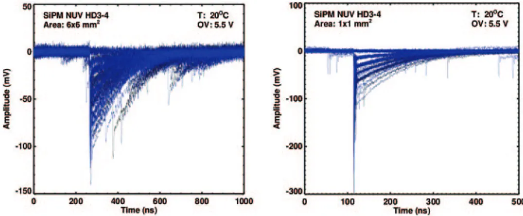
Fig. 4. – Left: example of superimposed signals from 6× 6 mm2 NUV-HD3 sensor. Right: example of superimposed signals from 1× 1 mm2 NUV-HD3 sensor.
Fig. 5. – Left: dependence of the gain of the sensors for different bias voltages and working temperatures. Right: comparison of the gain estimation from a 6× 6 mm2 NUV-HD3 sensor and 1× 1 mm2 NUV-HD3 sensor (at 20◦C).
log-derivative of the characteristic function (IV -curve) of the sensor as follows:
(1) ∂ ln(I(V ))
∂V =
2
V − Vbr
as shown in the left panel of fig. 3. The cumulative distribution of the Vbr of all the
boards is shown in the right panel of fig. 3.
The response of all sensors under laser light pulses and in dark conditions has been tested (pedestal, S/N ratio, dark count rate and gain [3]) and the best performing boards have been selected to equip a possible upgrade of the camera of the SCT prototype (pSCT). To make the tests less sensitive to the high Dark Count Rate (DCR), they were made on 1× 1 mm2. As shown in figs. 4, 5, using 1× 1 mm2 SiPMs implies a lower level of DCR (due to the reduced area of the sensor, fig. 4) but do not affect the measurement of other quantities (for example the gain of the sensor, fig. 5).
01/17/2019) is currently taking data for commissioning and calibration of the camera.
∗ ∗ ∗
The authors acknowledge the support received from Progetto Premiale TECHE.it.
REFERENCES
[1] The Cherenkov Telescope Array Consortium, Science with the Cherenkov Telescope Array, arXiv:1709.07997v2 [astro-ph.IM] 2017.
[2] Benbow W. et al., arXiv:1610.03865, [astro-ph.IM] 2016. [3] Ambrosi Giovanni et al., Nuovo Cimento C, 40 (2017) 78. [4] Ambrosi G. et al., SPIE Proc., 10392 (2018) 40.