U
NIVERSITÀ DEGLI
S
TUDI DI
C
ATANIA
Dottorato di Ricerca in Scienza e Tecnologia dei Materiali - XXVI ciclo
Salvatore Cosentino
Germanium Nanostructures for
Efficient Light Harvesting Devices
Tutor: Prof. A. Terrasi Supervisor: Dr. S. Mirabella
Coordinatore: Prof.ssa M.G. Grimaldi
COVER
TOP: Schematic illustration of a metal-insulating-semiconductor
photodetector with an active layer of Ge quantum dots embedded in SiO2. More details can be found within this thesis in section 4.3.
LEFT: Cross sectional Transmission Electron Microscopy of Ge quantum dots embedded in SiO2 matrix. More details can be found within this thesis in section 3.2.2.
RIGHT: Absorption spectra of single amorphous Ge quantum wells of different thicknesses. More details can be found within this thesis in section 2.1.1.
Germanium Nanostructures for Efficient Light Harvesting Devices
Salvatore Cosentino
Ph.D. Thesis, University of Catania Printed in Catania, December 2013
Out of the night that covers me, Black as the Pit from pole to pole, I thank whatever gods may be For my unconquerable soul. In the fell clutch of circumstance I have not winced nor cried aloud. Under the bludgeonings of chance My head is bloody, but unbowed. Beyond this place of wrath and tears Looms but the Horror of the shade, And yet the menace of the years Finds, and shall find, me unafraid. It matters not how strait the gate, How charged with punishments the scroll. I am the master of my fate: I am the captain of my soul.
Contents
Abstract ... I
Chapter 1
Nano for Energy ... 1
1.1 Global Energy demand: The TW challenge ... 1
1.1.1 Solar Energy ... 3
1.1.2 Sunlight-energy conversion ... 6
1.1.3 New approaches for efficient light conversion ... 10
1.2 Exploiting Quantum Confinement Effects ... 14
1.2.1 Playing with Quantum Confinement ... 15
1.2.2 Beyond bandgap tuning ... 20
1.3 Germanium: a promising material for light harvesting ... 24
1.3.1 Light Absorption Modulation ... 27
1.3.2 High efficiency photodetectors... 29
1.3.3 Group IV nanostructures solar cells ... 31
2.1 Light Absorption: from bulk to confined materials ... 39
2.1.1 Tauc model ... 44
2.1.2 The effects of confinement ... 46
2.2 Synthesis and structural characterization of amorphous Ge QW 48 2.2.1 Light absorption in single amorphous Ge QW ... 52
2.3 Quantum confinement in single amorphous Ge quantum wells .. 56
2.4 Conclusions ... 61
Chapter 3 Light Absorption in Germanium Quantum Dots ... 62
3.1 From 2D to 0D structures: when not only size matters! ... 63
3.2 The role of the size ... 66
3.2.1 Structural and optical properties of Ge QDs synthesized by sputtering ... 66
3.2.2 Ge quantum dots by PECVD ... 75
3.2.3 Quantum confinement: a solo player? ... 79
3.3 The role of the distance ... 83
3.3.1 Experimental design ... 83
3.4 The role of the matrix ... 91
3.4.1 Ge quantum dots by ion implantation ... 92
3.4.2 Ge QDs by PECVD: similarities and differences with the implanted case ... 97
3.4.3 SiO2 vs Si3N4 matrix ... 99
3.5 Conclusions ... 102
Chapter 4 Light detection with Ge nanostructures... 106
4.1 From material to device ... 107
4.2 The simplest approach: Light detection by single Ge QW ... 109
4.3 High efficiency photodetectors based on Ge QDs ... 113
4.3.1 Photoconductive Gain Mechanism ... 119
4.4 Tuning the optical response: the role of size and defects ... 124
4.5 Conclusions ... 136
References ... 138
List of Publications ... 146
Curriculum Vitae ... 149
The growing World energy demand is setting new challenges toward the use of alternative and green resources as well as for the development of more efficient and low-power consuming devices. Thanks to their unique optical properties, group IV (such as: Si, Ge, C) nanostructures (NS) show promising applications for cheap multi-junction solar cells and, in general, for efficient energy-tunable light harvesting devices. Among them, Ge reveals interesting optical properties due to its quasi-direct bandgap and larger absorption coefficient that make it intrinsically more suitable than Si for what concerns light harvesting applications. Moreover, the larger exciton Bohr radius of Ge (~24 nm) with respect to Si, gives the chance to easily tune the optical properties of Ge NSs by varying their size. However, the properties of Ge NS depends not only by size through quantum confinement effects, but many other parameters can concur in controlling their optical behavior, especially for what concerns the optical bandgap.
Discerning the role of these parameters and controlling their effects in the light absorption process contains not only a fundamental research theme, but represents a key-factor toward the implementation of Ge NS in any type of light harvesting device. For this reason, this thesis reports a detailed study on the synthesis, structural and optical properties of Ge nanostructures (quantum well, QW, or quantum dots, QDs) embedded in a dielectric matrix as well as the investigations of photo-conduction properties in prototypal light harvesting devices employing Ge NSs. Although the optical behavior of a single amorphous Ge QW can be fully modeled within the quantum confinement effect theory, this situation dramatically changes for a 3-dimensional confinement, as in an ensemble of QDs. In this last case, the effects of quantum confinement can be hidden or weakened by other parameters, such as: QD spacing and distribution, type and quality of the hosting matrix and abundance of defects related to the
II
synthesis technique used. For this reason, we will investigate in detail the synthesis and optical properties of Ge QDs embedded in SiO2 or Si3N4 matrices, grown after thermal annealing of Ge-rich films synthesized by co-sputtering deposition; plasma enhanced chemical vapour deposition (PECVD) and ion implantation. We will give evidences of the strength of quantum confinement effects occurring in these systems as well as discerning the contributions coming from other concomitant effects. Finally, we will demonstrate that Ge nanostructures can be effectively used as active absorber and conductive medium in light harvesting devices. In particular, we will report on the spectral response of metal-insulating-semiconductor (MIS) photodetectors employing a single amorphous Ge QW or a packed array of Ge QDs as active light sensitizer and conductive medium. Both types of NSs have a fundamental role on the performances of these prototypal devices, demonstrating the large potentiality of such nanostructures for the development of high efficiency photodetectors and low cost solar cells.
Chapter 1
Nano for Energy
1.1 Global Energy demand: The TW challenge
The Energy issue has always dealt a leading position in the economy and development of human society. The energy consumption of a country is directly related to both its economic output and the individual quality of life of its citizens. Both population growth and the desire to maintain and increase our current standards of living result in an increased energy consumption. In fact, the current global primary energy consumption per year is estimated to be of about 16 TWy (corresponding to ~
J TWh 20 5 5.4110 10 45 .
1 ), with a yearly growth rate of about 3% that will led to a doubling of energy demand in next twenty years, as reported in figure 1.1 [1], [2].
Fig 1.1: World primary energy consumption by fuel type in Mtoe
(million tonnes of oil equivalent) (from ref. [1], [2]. The category “Other” includes geothermal, solar, wind and heat. Note that 1 Mtoe is equivalent to 4.476×10¹⁶ J = 12 TWh)
2
Feeding, clothing and housing a continuously growing world population will be a significant challenge in terms of energy sustainability. In fact, the growing global energy demand, combined with the durability problem of supplying from fossil fuels, is setting new economic, politic and environmental problems. Today, almost 90% of the global energy is produced by burning coal, oil, natural gas or using nuclear plants [1]. These traditional technologies have strong potential impact on environment, both for the global growing threat of pollution and for the potential risk for the people and the economy of the affected areas (e.g., the Chernobyl and Fukushima nuclear disaster of 1986 and 2011 respectively, the Gulf of Mexico oil spill of 2010). Moreover, the rapid increase of the energy price, also favoured by financial speculations, has been one of the main reason of the recent international economic crisis. Last but not the least, the large quantities of carbon dioxide released in the atmosphere by the consuming of fossil fuels are causing strong consequences for the climate balance of our planet.
Figure 1.2: Power requirements for different applications [3].
An interesting marker of the growing energy demand is given by the rapid growth of personal and mobile electronics devices, which profoundly entered in our daily life. Individually, the power consumption of these technologies is rather low: from some µW to W per single electronic device, as shown in figure 1.2. However, the number of such devices, integrated over the entire world population consumers, is huge and is expected to
3
increase with the standards of human living. Moreover, the powering of most electronic devices still relies on rechargeable batteries. Of course, the amount of required batteries increases in proportion with the increase of the number and density of electronic devices. This may result in challenges for recycling and replacement of the batteries (usually made of environmentally unfriendly and cost-effective products) as well as an increased energy consumption.
Therefore, our future quality of life greatly depends on how successful we are in developing a sustainable energy technology that can meet our future energy needs. The development of novel materials and innovative technologies to replace the traditional oil and carbon fuels will be a milestone in the future research and political agenda. In this scenario, solar energy could be a viable and environmentally conscious solution to the growing global demand for energy. Moreover, also the development of high-efficiency and low-power consuming devices is highly desired for a better energy consumption. For this reason, a focus of active research in this field is the exploration and the study of new materials to enhance the performance of more efficient energy harvesting devices.
1.1.1 Solar Energy
Energy from the Sun is the basis of life on Earth. Both active (i.e. solar cells) or passive (i.e. green houses) solar energy harvesting have always been close to human development. Solar energy is by far the most abundant and sustainable source for Earth. Figure 1.3 compares the current annual energy consumption of the world to the known planetary reserves of fossil fuels and nuclear resources and to the yearly potential of the renewable alternatives [4]. The solar resource is orders of magnitude larger
4
than all the others combined. More energy is provided to the Earth by sunlight irradiation within one hour than is consumed by human society globally in one year.
Figure 1.3: Comparing finite and renewable planetary energy reserves
(Terawatt-years). Total recoverable reserves are shown for the finite resources. Yearly potential is shown for the renewable sources [4].
The energy output from the Sun that reaches the Earth can be calculated by applying some fundamentals rules of Physics. As shown on Figure 1.4, the spectral irradiance I(λ) of Sun outside the Earth’s atmosphere can be approximated to the spectral thermal radiation of a blackbody emitter held at a temperature T of about 5800 K, given by Planck’s formula: 1 2 ) ( 5 2 T k hc B e hc I
(1.1)5
where h is the Planck’s constant, c is the speed of light and kB is the
Boltzmann constant. The terrestrial atmosphere attenuates the sunlight, mainly because of the water-vapor and ozone absorption or by scattering phenomena. The degree to which the atmosphere affects the sunlight is quantified by the air mass unit, defined as the secant between the sun and the zenith (AM 1/cos
). Thus, AM0 represents the solar spectrum outside the earth’s atmosphere, while AM1.5 (commonly used as a standard reference for solar cell efficiency) represents the sunlight at the Earth’s surface when the sun is at
48.2from zenith.Figure 1.4: Solar spectrum in photon flux density per photon energy for
AM0 and AM1.5 conditions, together with the black body radiation spectrum at 5800 K [5].
Integrating I(λ) over all wavelengths gives a power density of about 63.3 MWm-2 [2]. Considering that the intensity of electromagnetic waves decreases with the inverse square of the distance from the source, we can estimate an irradiance of as 1327 Wm-2 reaching the Earth’s atmosphere. From this value, one can estimate an average of about 35000 TW arriving just above the Earth atmosphere. This is an enormous amount of energy,
6
even if we take into account of the attenuations due to the scattering and optical absorption of the incident light by the atmosphere, which reduce the incident energy to around 23000 TWy. Thus, the exploitation of even a very small fraction of the Earth’s solar potential could meet the global energy demands. Sunlight-electricity conversion devices exploiting photovoltaic (PV) effect have experienced a rapid development in the past few decades. PV market has shown annual growth rates between 40% and 90% since 2000 [6], with strong similarities with the Moore’s law for the integrated circuits. In sharp contrast to the huge amount of energy we receive from the sun, only less than 0.1% of the total energy production (about 80 GW by the end of 2012) comes from the sunlight conversion [6]. This is mainly due to the fact that the existing PV technologies have yet not been able to produce electricity at a comparable price with conventional generation methods. In this regard, a lot of efforts have been invested toward development of PV technologies that operate with enhanced efficiency and lower cost. In this scenario a key-role is represented by the research on new materials and optimized device structure to increase the performances and reduce the fabrication costs of these devices.
1.1.2 Sunlight-energy conversion
As a result of a photoelectric-based phenomenon, the exploitation of solar energy in PV devices relies on two basic steps: photon absorption and photo-carrier collection. In nearly all types of solar cells the absorber medium is a semiconductor. Figure 1.5 illustrates the principle of a conventional single p-n junction solar cell. Incident photons that have energies above the semiconductor bandgap (Eg) are absorbed, creating
electron-hole pairs. These electron-hole pairs are separated and collected at the output of the PV device through the action of an electric field, giving
7
rise to an external power. Such electric field is usually created by a p-n junction (connection of p- and n-type doped semiconductor, figure 1.5) or Schottky junction (connection of a metal and a doped semiconductor).
Figure 1.5: Schematic diagram of a conventional single-junction
semiconductor solar cell. Absorbed light with photon energies greater than the bandgap produces carriers, electrons and holes. Loss processes are: non-absorption of below-bandgap photons, heat losses, and radiative recombination. Adapted from ref. [7].
A conventional p-n junction solar cell is assumed to have a ideal diode I-V characteristics. When such a device is illuminated, the total I-V characteristics can be written as a summation of the dark diode current and the photocurrent IL due to generated electron-hole pairs.
L s
I
kT
qV
I
I
exp
1
(1.2)where Is is the diode saturation current [5].
From eq. (1.2), we obtain the open-circuit voltage by setting I = 0, while the short-circuit current Isc represents the photocurrent extracted at V = 0. The I-V characteristic under illumination passes through the fourth
quadrant and, therefore, power can be extracted from the device to a load. We can define the quantities Im and Vm that correspond to the current and
8
the voltage that maximize the power output P m ImVm. In this regard, the
ideal conversion efficiency of a solar cell is defined as the ratio of the maximum power output to the incident light power Pin:
P /m Pin.Large part of the current photovoltaic technology utilizes single p-n junctions of mono- or poly-crystalline bulk silicon or thin films of amorphous silicon, cadmium telluride (CdTe), or copper indium gallium selenide (CIS) as active absorber. The semiconductor material has to be able to absorb a large part of the solar spectrum, which is primarily determined by its bandgap, and at the same time guarantee an efficient photo-carrier extraction. Nevertheless, the requirements to optimize both optical absorption and carrier collection can be in conflict. For example, in a standard p-n junction solar cell, a thick material (~µm) is needed to achieve a consistent fraction of photon absorbed. However, this can lead to a lower photo-carrier collection because of the increased path for minority carriers and the resulting larger probability of electron-hole recombination, and vice versa. In principle, a thin active layer (~100 nm thick) of a material with high absorption coefficient (>105 cm-1) would be largely desired to reduce the production costs and maintain high photo-carrier collection capability.
Indeed, the sunlight-electricity conversion process in p-n junction solar cells suffers of some intrinsic losses that strongly limit the efficiency in these systems. As illustrated in figure 1.5, the primary losses in a p-n junction solar cell are: photons with energy below the semiconductor bandgap do not contribute to electrical current (sub-bandgap losses);
thermalization losses of photons with energy exceeding the bandgap and radiative recombination of electron-hole pairs. Considering these
limitations, the maximum thermodynamic efficiency for single bandgap devices is about 31%, according to the detailed balance limit of Shockley– Queisser (SQ) [8].
9
Figure 1.6: Yearly trend of solar cells record efficiency. Different colors
and symbols define the different generations and technologies [9].
Figure 1.6 shows the evolution of efficiency for various solar cell technologies over the last three decades. Up to date, the highest 1-sun efficiency of a single crystal (sc) sc-Si cells is ~25%, while that of polycrystalline Si (poly-Si) cells is 20.4%. The record efficiency for all solar cell technologies is held at 41.6% by triple-junction solar cell. This cell stacks three p-n junctions made of GaxIn1-xAs or GayIn1-yP with different compositions. Each junction has a different band gap and is responsible for light absorption in a certain portion of the solar spectrum. The efficiency is measured with a concentrator under 326 Suns. Under one Sun, the efficiency of this triple-junction cell is 33.8%. Besides wafer Si, several thin-film solar cell technologies have been commercialized, including Si in either amorphous (a-Si) or microcrystalline (μc-Si) form and metal chalcogenides
10
(CdTe and CuInxGa1-xSe2 (CIGS)). Their record efficiencies range between 12% and 20%.
While the progress in the efficiencies of these solar cells has been remarkable, new approaches are needed in order to boost the performance of these devices beyond the SQ limit. Closing (and overcoming) this efficiency gap is the main subject of ongoing PV research. In this regard, new approaches in the light absorption management and in the optimization of the photocarrier extraction would be largely desired for the development of more efficient solar cells.
1.1.3 New approaches for efficient light conversion
As described previously, one of the main limit of current PV technology are intrinsically connected with the capability of the material to absorb the incident light. In this regard, several possible strategies have been put forward to reduce sub-bandgap and thermalization losses and achieve higher conversion efficiencies.
In multi-junction approach (figure 1.7a), the use of several band-gap materials allow to convert different portions of the spectrum, reducing the thermalization and the sub-bandgap losses. Multi-junction solar cells are made in a series- or parallel- connected architecture, with each sub-cell acting as a ‘filter’ and absorbing only above-energy bandgap photons. The detailed balance limit for optimized multi-junction cells under 1 Sun illumination shifts from the SQ limit to 42%, 49% and 53% for 2, 3, and 4 cells, respectively. For the hypothetical system with infinite number of sub-cells the limit efficiency is 68.2%. Triple-junction solar cells made of
11
GaInP/GaAs/InGaAs or GaInP/GaInAs/Ge already demonstrated record conversion efficiencies of over 40%, as shown in figure 1.6) [9]. However, the disadvantage of this approach relies on the complexity and the high cost of the structure that limit its applicability on large scale.
In intermediate band (IB) approach (figure 1.7b), sub-bandgap energy photons can be absorbed by intermediate energy levels located in the forbidden gap. In this way, sub-bandgap energy photons are absorbed through transitions from the valence band (v.b.) to the intermediate band (IB) and from the IB to the conduction band (c.b.), enabling, at least in principle, IBSCs to achieve both high current and high voltage. The theoretical limiting efficiency of IB solar cells is 63% under 1 Sun isotropic illumination [7]. The principal ways to obtain IB is by introducing in the host semiconductor extended defects, impurities, mismatched alloys, or superlattices of quantum dots. However, the main issue of this approach is achieving a strong absorption from IB without increasing non-radiative recombination processes. In addition, IB must be electronically separated from valence and conduction bands, otherwise the photo-voltage would be reduced.
In carrier multiplication approach (figure 1.7c), one high energy photon excites two or more lower energy excitons. Such an inverse Auger process is usually called multiple exciton generation (MEG) and has been observed in bulk semiconductors (such as Si-Ge alloys) as well as in quantum dots (PbSe, CdTe, CdSe, Si) [11][12][14]. This process is inefficient and not exploitable in bulk semiconductors because the MEG rate is much slower than radiative recombination process and also because high energy photons lying outside the solar spectrum (E > 3.5 eV) are needed to
12
create extra carriers in bulk semiconductors. It was proposed that MEG process might be more efficient in quantum dots made from Si, PbSe, InAs and CdSe. Numerous experiments have confirmed the existence of MEG in these systems [11], [12][14]. However, multi-excitons tend to recombine very fast (ps time scale), limiting the carrier extraction process in a future device.
In wavelength conversion approach (figure 1.7d), several low energy photons are converted into one high-energy photon
(up-conversion) or, alternatively, one high-energy photon is divided into
several low-energy photons (down conversion). These approaches enable to reduce losses due to transmitted light or thermalization processes, respectively. The incident spectrum can also be modified by down shifting photon process, where one high-energy photon is absorbed by a luminescent center and then re-emitted at a longer wavelength. Most data on this approach have been achieved using rare-earth ions such as Er3+, Yb3+, Eu3+ based compounds [15], [16]. The disadvantage of this approach relies on the low optical cross section of radiative transitions and on the relatively narrow bands of absorption as well as the very high cost of rare-earth elements.
13
Figure 1.7: Main approaches for new generation PV cells: (a)
Multi-junction; (b) intermediate-band solar cell; (c) Carrier multiplication process (called impact ionization in bulk semiconductor); (d) wavelength conversion for “shaping” of the incoming solar radiation.
14
As evident from the above examples, the improvement of the performances in light harvesting devices largely relies both on the optimization of photon absorption and photo-carrier extraction mechanisms. However, the simultaneous optimization of both processes is non trivial for solar cells based on conventional structures, also for the needing to maintain low fabrication costs. Efficiency and cost can be considered as the two sides of the same coin. Any efficiency improvement is often accompanied by additional costs, so it has to be done in a cost-effective manner.
In this regard, the exploitation of novel physical properties in “new
materials” could meet the requirements of optimized light-conversion
efficiency and low production costs. In particular, the usage of semiconductor nanostructures and the exploitation of their unique optical and electrical properties have been proposed as possible solution not only for boosting energy-conversion efficiency beyond the actual SQ limit of conventional solar cells, but also for the development of novel high efficiency optoelectronic devices and light harvesters.
1.2 Exploiting Quantum Confinement Effects
The field of Nanotechnology has seen an extraordinary explosion of interest in the few decades, particularly due to the possibility to exploit the fundamental rule of quantum mechanism in many applications. The seminal event of the Nanotechnology era is considered to be the famous talk “There is Plenty of Room at the Bottom” given by the physicist R. Feynman at the annual meeting of the American Physical Society at Caltech on 29th December, 1959 [17]:
15
“Now, the name of this talk is "There is Plenty of Room at the Bottom" – not just "There is Room at the Bottom." What I have demonstrated is that there is room – that you can decrease the size of things in a practical way. I now want to show that there is plenty of room. […] Atoms on a small scale behave like nothing on a large scale, for they satisfy the laws of quantum mechanics. So, as we go down and fiddle around with the atoms down there, we are working with different laws, and we can expect to do different things. […] At the atomic level, we have new kinds of forces and new kinds of possibilities, new kinds of effects. […] The principles of physics, as far as I can see, do not speak against the possibility of maneuvering things atom by atom. It is not an attempt to violate any laws; it is something, in principle, that can be done; but in practice, it has not been done because we are too big.”
The study and application of nanostructures have the interest of many generation of scientists up to now, giving origin to what it is now known as nanotechnology. Due to strong changes of structural, electrical, optical and chemical properties of materials at the nanoscale length, nanotechnology opened the way to a new era in many fields, most of which have a huge impact on our current the daily life, from nano-optoelectronic [18] [19] nano-biology [21], chemical sensors [20] to new concepts for high efficient light harvesters and solar cells [22] - [24].
1.2.1 Playing with Quantum Confinement
A nanostructure (NS) is, for definition, any material which spatial dimensions are confined to the nanometer scale (1 - 10 nm). In the
16
following paragraphs, we will refer to NS based on semiconductor materials. If the dimension of the system becomes comparable or smaller than the Bohr radius rB of charge carriers (
r
B
a
0
/ m
*, where
is thedielectric constant and m* the reduced mass of carriers), the carries “feel” the confinement due to the boundaries of the material and are said to be confined. This phenomenon, which is known as quantum confinement
effect (QCE), dramatically changes the valence and conduction bands of the
system [25]. As drawn in Figure 1.8 (a), when the carriers are spatially confined in one dimension the system is defined as quantum well (QW), a two dimension-confinement produces a quantum wire (Q-wire), while a confinement in all the three dimensions confinement structure is defined as quantum dot (QD). Nanostructures can be successfully modeled as a particle in a box model system by considering a nanometer size inclusion embedded in an insulating matrix with a potential barrier V, as shown in Figure 1.8(b).
Figure 1.8: (a) Schematic representation of quantum wells, wires and
dots. (b) Potential well formed in any dimension (x, y, or z) in the conduction and valence bands. The energy levels of the excited carriers (electrons and holes) become quantized due to the finite size of the nanostructure.
One of the most important property of a nanostructure is that by lowering the dimensionality, the energy levels of the systems collapse from
17
continuous energy bands, typical of bulk materials, into discrete energy levels. In particular, the density of states (DOS) and the energy levels for the different degrees of quantization are described by the following equations, valid in the case of an infinite potential barrier V:
E m E bulk 2 1 3/2 2 * 2 ;
2 *2 2m k k Ebulk
x x n n QW E E m E 2 * ;
*
2 2 2 2 * 2 2 2 2 2 m k k L m n k k E x y z y x n (1.3)
1/2 , , 1
y x x n n n Wire Q E E E ;
* 2 2 2 2 2 2 * 2 2 , 2 2 m k L m L n m k E x y z x m n
z y x z y x n n n n n n QD E E E , , , , 1 ; 2 *2 22 22 22 , , 2 z y x l m n L l L m L n m E where ki is the momentum vector, (E)is the step function, Li and Eni (with i=x,y,z) are respectively the system dimensions and the quantized energy
levels along the directions of confinement, while n, m, l N are the
quantum numbers. The energy values in equations (1.3) are offset by the bandgap energy value of the bulk semiconductor. A plot of the DOS for the different degrees of confinement is shown in Figure 1.9, considering Si as material (m*=1.08) and a confinement dimension Li of 2 nm [26]. The
decrease of system dimensionality strongly modifies the DOS and the energy occupation levels. In particular, more discrete and energy-spaced states can be found as the degree of confinement gets higher.
18
Figure 1.9: Plot of the DOS for a bulk (3D) or QW (2D), Q-Wire (1D) and
QD (0D) Si structures [26].
More generally, the bandgap Eg of a nanostructure (defined as
difference between the lowest unoccupied level in c.b. and the highest occupied level in v.b.) along the confinement direction can be modeled within the effective mass approach (EMA) theory by the following relation [25]:
* 2 2 2 2 ) ( L m bulk E NS Eg g (1.4)where
E
g(bulk
)
is the bandgap of the unconfined material and * 2 22m
A
is the confinement parameter. Eq. (1.4) is a simplified formula of the actual energy gap of a NS, since does not take in account of the corrective factors due, for example, to the electrostatic Coulomb interaction between electron and hole or the energy level splitting caused by the spin-orbit interaction. However, the magnitude of such factors usually produces variations from the values obtained by using Eq. (1.4) of the order of 10 - 50
19
meV. Eq. (1.4) shows that the bandgap of a NS is increased with respect to the bulk material by a quantity which is inversely proportional to the square of its size L and to the effective mass of the electron-hole pair m*. In
addition, the value of A is larger as more reduced the system dimensionality is, giving rise to a larger tuning of the band-gap with the size L. Moreover, Eq. (1.4) is valid in the case of an infinite confining barrier potential. In a real dielectric matrix with a finite barrier height V0, the value of Eg given in
Eq. (1.4) is reduced by the factor
2 0 * 2 1 V m r [27]. Hence, lower
potential barriers reduce the effectiveness of quantum confinement. The gap tailoring with NS size is one of the most important and potentially useful properties of a nanostructure, in particular for what concerns the light management in future optoelectronic devices and light harvesters. One of the most famous example of a light harvesting device based on the exploitation of QCE is the "all Si tandem solar cell", proposed by Green et al. [27], [28]. This solar cell consists in a multiple stack of QD-based cells where the Eg of each sub-cell is tuned with the QD size. Such a
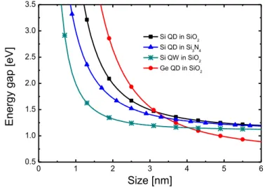
type of solar cell gives the possibility to absorb a larger portion of the solar spectrum, as in multi-junction solar cells, but using just one type of material with a potential high reduction of production costs. Actually, such a band-gap engineering can be performed not only by varying the NS size, but also playing with other parameters, like: the height of the confinement barriers where NS are embedded, the degree of confinement, the use different materials or alloys. As an example, Figure 1.10 shows the theoretical values of bandgap (calculated by using the values of A given in ref. [29]) for Si or Ge NS and the role played by the NS size, degree of confinement and embedding matrix. All these parameters strongly affect the effectiveness of the QCE occurring at the nanoscale, giving the chance to span more or less gently the optical band-gap over the entire UV-NIR range.
20 0 1 2 3 4 5 6 0.5 1.0 1.5 2.0 2.5 3.0 3.5 Ene rgy ga p [ eV] Size [nm] Si QD in SiO2 Si QD in Si3N4 Si QW in SiO2 Ge QD in SiO2
Figure 1.10: Theoretical size-dependent shift of the optical band-gap for
Si and Ge NS calculated by using the EMA relationship in eq. 1.4.
This means that, starting from a bulk system and playing with QCE, is possible to “create” totally new materials and finely engineer their optical properties. Such a possibility opens a new route toward the optimization of light management in novel nanostructure-based optoelectronics: from light emitting devices operating at telecommunication wavelengths to energy tunable light harvesters and multi-junction solar cells.
1.2.2 Beyond bandgap tuning
Besides the band-gap tailoring due to QCE, other important effects can lead to an increased light harvesting and improved performances in NS-based devices in respect to bulk systems. First of all, the reduction of the system dimensions leads also to the breaking of the k-conservation rule for
21
optical transitions. This effect is a direct consequence of the Heisenberg uncertainty relation. The confinement of electron-hole pairs in the real space causes a spread-out in the momentum space of their electronic wavefunction, as shown in figure 1.11 for the case of Si QW [26]. As the confinement dimension Lx is reduced, the dispersion in momentum space is
increased, resulting in a larger overlap of the electron-hole wavefunctions. This, in turn, leads to an increased optical transition probability between electron and hole states. This effect is particularly important for indirect gap materials, such as Si or Ge. In this kind of systems optical absorption/emission requires phonon scattering in order to maintain momentum conservation. Such a three bodies event (electron, hole and phonon) is significantly less probable than a direct band-to-band transition and result in a low optical transition probability, typical of indirect-gap bulk materials. However, due to the breaking of k-selection rule, optical transitions can happen without the assistance of phonons in NS, which implies an increased probability of radiative transitions.
Figure 1.11: Plot of a Gaussian envelope function for a single
confinement direction in k-space with an electron centred at 0.8 × X-point and a hole at the Γ-X-point in the Brillouin zone for Si. The plot is not normalized and is shown for three different confinement dimensions, Lx,
22
Therefore, the carrier confinement in NS produces also an increase of the oscillator strength of the optical transitions. This is because the transition probability depends on the coupling between states in the conduction (c) and valence (v) bands through the dipole matrix element:
2
c
p
v
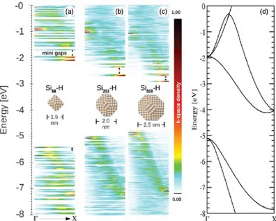
. Such a quantity increases as the dimension of the system is reduced, due to the larger wavefunction overlap of electron-hole pair, as depicted in Figure 1.11 [26]. A detailed theoretical and experimental discussion of the enhanced oscillator strength occurring in NS will be given in chapter 2.Another important effect derived from the overlapping of confined levels in NS is the formation of minibands in closely packed array of NS. Such effect has been extensively studied for application in IR photodetectors, resonant tunneling diodes, as well as intermediate band solar cells [30] - [31][32]. In particular, the coupling among quantum dots leads to a splitting of the quantized carrier energy levels of single dots and formation of three-dimensional minibands. Very recently, Hu et al. demonstrated that the formation of minibands in Si QD superlattices (QDS) embedded in SiO2 or SiC strongly enhances both optical and electrical collection [33]. As shown in figure 1.12 (a), the lower band-offset between QD and embedding matrix increases the wavefunction overlapping between adjacent QDs, inducing additional optical transitions [31], [33]. In addition, the classic quantum confinement effect provide the possibility to further engineering the electronic band structure of this QD-based material by changing QD size, QD-QD distance or barrier height. As shown in figure 1.12 (b) and (c), miniband energy position decreases inverse-squarely with increasing size of QDs, while the inter-dot spacing affects the miniband width (figure 1.12d).
23
Figure 1.12: (a) Ground-state electron wavefunction distribution in the Si
ND superlattice embedded in a SiC matrix and SiO2 matrix. (b) Systematic miniband engineering diagram in Si QDs embedded in the SiC matrix. Minibands dependence on (c) Si QD diameter and (d) inter-dot space distance for different quantum numbers. Adapted from ref. [33].
Therefore, the usage of nanostructured materials allows not only to properly engineer the bandgap via QCE, but also enables the chance to overcome the current optoelectronic limitations of bulk Si and Ge semiconductors and to strongly enhance the light absorption/emission process in these materials. Thus, the exploitation of the optical and electronic properties of nanostructures could open a route for the development of high-performance optoelectronic and light harvesting devices.
In this regard, a key-factor toward an easier implementation of nanostructures in novel devices is the compatibility with the current Si
24
technology. For this reasons, a lot of efforts among scientific community have regarded the investigation of the structural and optoelectronic properties of group IV materials (such as Si, Ge, C). While a lot of research exists on Si NS ([34]and references therein), Ge NS have been often under-rated because of the lower abundance, higher costs and poor oxide quality of the bulk Ge. However, Ge evidence even better potentiality than Si at the nanoscale, in particular for what concern the bandgap tuning and the capability to absorb light. In the following paragraphs, the main properties of Ge will be shown as well as the state of the art regarding the exploitation of the optical properties of Ge NS in novel optoelectronic and light harvesting devices
1.3 Germanium: a promising material for light
harvesting
Germanium (Ge) played a primary role since the beginning of the solid state electronics age. The first transistor, invented at Bell Laboratories in 1947 by William Shockley, John Bardeen and Walter Brattain, was fabricated on crystalline Ge substrate [35]. However, the usage of such material in microelectronic industry has been limited only to some niche markets. This is historically due to the poor quality and high instability of the Ge oxide (GeO2) that limited its use in complementary-metal-oxide-semiconductor (CMOS) technology in favor of Si. In addition, another large drawback regards the material availability. In contrast to Si, the second most abundant element on Earth’s crust (27.7%), Ge is pretty rare and widely dispersed (~6.7 parts per million [36]). For these reasons, a large-scale use of bulk Ge in microelectronic industry would be very challenging and cost-effective.
25
Recently Germanium gained a renewed attention because of its attractive properties that can provide solutions for some of the major issues of silicon toward the development of miniaturized and high-efficiency devices and optoelectronic devices.
Figure 1.13: (a) Primitive cell relative to the diamond lattice
characteristic of Si and Ge crystals. In this configuration each atom is bonded with other four identical atoms placed at the corner of a tetrahedron. The lattice constant of the cell is indicated with a. (b) Representation of the energy-k dispersion of Ge calculated by the k•p method [5].
One of the most important features of Ge regards its high compatibility with the current Si technology. In fact, both Si and Ge belong to the group IV of elements and have the same crystalline diamond-type structure [see figure 1.13 (a)]. The diamond structure consists of two interpenetrated face centered (FCC) lattices having a the lattice parameter
a. The same crystalline structure and the similar values of a in Si (0.5657
nm) and Ge (0.5431 nm) lead to a fully miscibility of these two elements over the complete concentration range and for a sufficiently large atomic fraction [36]. This has important consequence for the optoelectronic properties of SiGe alloys [37]. In fact, the strain related to the lattice mismatch between Ge and Si (~4.2%) allows to engineer the bandgap by varying the concentration of Ge in Si (or vice versa). Figure 1.13(b) shows the energy-k dispersion calculated by k•p method for bulk Ge. Relaxed bulk
26
Ge has an indirect gap of ~0.67 V at the L valley and a direct gap of 0.8 eV at the Γ valley (k = 0). When a biaxial tensile stress is applied, Ge changes from an indirect to a direct gap material with the increase of tensile strain and its capability to absorb/emit light are greatly enhanced [38] - [41]. The engineering of Ge bandgap through tensile strain gives the possibility to develop novel optoelectronic devices (such as LED, laser, optical modulators, etc) fully compatible with Si technology [37] - [41].
Moreover, Ge absorbs light much better than Si. As shown in figure 1.14, the absorption coefficient of crystalline Ge is more than one order of magnitude larger than Si up to 3 eV. This peculiarity is related to the lower value and the nearly-direct nature of its band-gap with respect to Si. The capability to absorb light also in NIR range (where bulk Si is optically blind), combined with its high carrier mobility (related to the lower m* for
electrons and hole in Ge [36]) proposed Germanium as a viable candidate for the fabrication of IR photodetectors, high-speed optical modulators as well as high efficiency multi-junction solar cells [38]- [42].
1 2 3 4 5 103 104 105 106 Abso rptio n coe ff ici en t [cm -1 ] Energy [eV] Silicon Germanium
Figure 1.14: Absorption coefficient of crystalline Silicon and Germanium,
27
For the above mentioned properties, Ge is intrinsically more suitable than Si for what concerns the capability to absorb light. However, the usage of such material in the bulk form has been quite limited in the past because of the high production costs. In this regard, the usage of Ge in form of nanostructures could meet the scarcity issue of this element, giving also the chance to exploit the QCE occurring in these systems. In particular, Ge shows an exciton Bohr radius (~24 nm) well larger than that of Si (~ 5 nm) [43]. This means that it should be possible to easily tune the absorption edge of Ge NS from the IR across the visible range without the needing to shrink too much the NS size, as already shown in figure 1.10.
Such opportunity, together with the larger absorption capability and the quasi-direct bandgap of Ge, make Ge NS very attractive for the application in a large variety of devices, spanning from energy-tunable light harvesters (e.g. multi-junction solar cells and photodetectors) to efficient optoelectronic devices. In the following paragraphs an overview of the state of the art regarding the exploitation of such properties most interesting properties of Ge NS and their possible applications will be shown. These include: optical modulators, efficient photodetectors and solar cells.
1.3.1 Light Absorption Modulation
Modulating light absorption is an essential characteristic for the development of novel Si-compatible optoelectronic devices for telecommunications and computer interconnections. High-speed silicon optical modulators based on metal-oxide-semiconductor capacitor have already been demonstrated, but because the light modulation mechanisms in silicon are relatively weak, several mm-long devices or sophisticated high-quality factor resonators have been necessary [44]. A successful approach toward the fabrication of optical modulators is to exploit the quantum confinement Stark effect (QCSE) occurring in confined system.
28
QCSE is a strong change of the optical absorption of a material when an external electric field is applied. Such effect is typically observed in III/V semiconductor quantum wells, due to their strong direct optical transitions [45]. However the demonstration of QCSE, in a silicon-compatible materials such as Ge QWs could open up many new possibilities for electrical modulation of light absorption [46]. In fact, though germanium has an indirect bandgap (~0.67 eV), it is possible to exploit the stronger optical transitions associated to its direct bandgap at 0.8 eV.
Figure 1.15: (Top figure) Side-entry optoelectronic modulator schematic.
(Bottom figure) Strong QCSE is observed at room temperature with reverse bias from zero to 4V. The inset shows the cross-sectional view shows the structure of strained Ge/SiGe multiple quantum wells (MQWs) grown on silicon on relaxed SiGe direct buffers. Adapted from [46], [47].
As shown in the inset of figure 1.15, strong QCSE have been demonstrated in strain balanced Ge/SiGe multiple QWs (QW 10 nm thick)
29
grown on a relaxed Ge-rich SiGe buffer layer on Si in a p-i-n configuration [46]. When an electric field is applied a clear shift due to QCSE occurs. In particular, the absorption curve at zero bias (0 V) consists of two exciton peaks at 0.88 and 0.91 eV, corresponding to the heavy hole and light hole to Γ electron transitions. The strong electric field provided by the applied voltage produces a shift of the electron states toward lower energies, while the hole states shift to higher energies. This produces a shift of the absorption edge to lower energies, as shown in Figure 1.15. The strong electro-absorption observed in Ge/SiGe multi QWs is comparable to that of QCSE III/V QW structures and is very promising for electro-absorption modulators operating at high speed, low power and operating voltage and with small device areas.
1.3.2 High efficiency photodetectors
Due to its high absorption coefficient in the NIR region and the advantage of ease integration with Si, photodetectors based on bulk Ge has been already largely utilized for light detection in the telecommunication wavelength range of 1300 - 1600 nm, but the cost and the device speed are issues. In recent years, various configurations of thin-film Ge-based photodetectors (p-i-n, waveguide coupled or avalanche gain detector design) have been developed and demonstrated high values of performance (0.5 - 1 A/W at 1550 nm) [38]. However, further miniaturization of the components design and optimization of the performance at low or zero bias is essential to achieve high energy efficiency and reduced costs for a large-scale electronic-photonic integration. In this scenario, the discrete levels produced in Ge NS by quantum confinement can guarantee promising applications for light detection in narrow spectral IR and compatibility with CMOS technology as well as reduce production costs. In particular, due to the band offset at the
30
Ge/Si heterojunction, discrete energy levels can be formed inside Ge at the nanoscale. With this approach, different configurations can be used to extend the cut-off wavelength and exploit the absorption between discrete states in Ge QDs. For example, metal-semiconductor-metal photodetectors having a Ge QDs/Si ML as active region already demonstrated potentiality at 1.3 and 1.55 μm, with responsivity of about 0.1 A/W [48]. The use of Ge QDs in waveguide-coupled p-i-n photodetectors showed a larger photoresponse compared to p-i-n Si photodetectors, with responsivity of ~210 mA/W at 1.3 μm (see figure 1.16b). Another study on metal–oxide– semiconductor (MOS) tunneling photodetectors with Ge quantum dots embedded in the Si semiconductor region showed high responsivity (~600 mA/W) at 820 nm, but only a limited photoresponse (< 1 mA/W) in the NIR [49].
Figure 1.16: (a) Schematic structure of MIS SiGe/Si QD photodetector
[48]. (b) NIR response of a silicon p-i-n photodetectors with Ge/Si QDs multilayer in the intrinsic region. The response of a silicon p-i-n photodiode is given for comparison [50].
Though QD-based photodetectors show promises for integration in CMOS technology, further efforts are required to improve the performances towards successful fabrication of sensitive imaging systems.
31
Only recently, MOSFET-like PDs based on Si QDs embedded in the oxide layer showed responsivity up to 2.8 A/W at 1.55 µm and an internal photoconductive gain efficiency of 200% [51], [52], whereas Ge QD-based PDs reached even higher photoresponse in the VIS region with photo-conversion efficiency of ~400% [53][54]. We recently reported on MOS PDs with a ~250 nm active layer of 2 nm-diameter amorphous Ge NCs in SiO2 with even better performance: very high values of responsivity (up to 4 A/W) and quantum conversion efficiencies up to 700% in the VIS-NIR wavelength range [55]. In addition, this type of PD demonstrated to achieve a time response down to ~40 ns, with minimal loss in responsivity [56]. These results open new fascinating routes toward the development of high-efficiency light harvesters based on Ge QDs and will be extensively investigated on chapter 4.
1.3.3 Group IV nanostructures solar cells
Quantum dots have attracted much attention for their possible use in photovoltaic applications because of the potentiality to overcome the limits of conventional single-junction devices. In particular, by exploiting the size-dependent band-gap tuning that occurs in confined system is theoretically possible to increase the fraction of absorbed light from solar spectrum in multi-junction QD-based solar cells. For a terrestrial solar spectrum (AM1.5G, 1000 W m−2) the optimal band-gap of the top cell required to maximize energy conversion efficiency is 1.7–1.8 eV for a two-cell tandem combined with a crystalline Si (c-Si) bottom cell [5]. Cho et al. demonstrated solar cells consisting of phosphorus-doped Si QDs in a SiO2 matrix deposited on p-type crystalline Si substrates (c-Si) have demonstrated conversion efficiency of about 10%, with open-circuit voltage (Voc) increasing
proportionally with the reduction of QD size [57]. However, up to date, all the reported experiments on such a type of cells evidenced a reduced Voc
32
cells, due to photocarriers recombination at the QD/bulk interface. In order to improve the light absorption in conventional solar cell and increase the overall conversion efficiency, especially in the IR part or the spectrum, another promising approach could be to use NS for intermediate band solar cells. Recently, p-i-n solar cells with the intrinsic layer composed by multilayers of Ge QDs embedded in Si demonstrated an enhanced conversion efficiency for λ> 1400 nm, reflecting the fact that the Ge QDs cause additional photon absorption at longer wavelengths of the solar spectrum [58], [59].
Figure 1.17: Comparison of the performances of solar cells with photonic
nanocrystals coupled with Ge QDs (PC), with Ge QDs only (QD) and the control CZ Si solar cell. The insets in (a) illustrate the fundamental structure and the band alignment of the device. Adapted from ref [60].
33
In addition, the performance of solar cells can benefit also of innovative design architectures. Very recently, an enhanced photon capture and carrier generation has been demonstrated in p-i-n solar cells employing two-dimensional photonic nanocrystals coupled with Ge QDs (see inset in figure 1.17a). As shown in figure 1.17, this type of solar cells showed a marked increase of the conversion efficiency with respect to a reference Si
p-i-n cell, due to the coupling of Ge QDs with photonic crystals that
guarantee an enhanced light trapping and photoconversion. Therefore, an optimized light management and a proper control of the optical and electronic properties of QDs-based solar cells can effectively boost the photo-conversion performance beyond the actual limit of conventional solar cells.
Though these results are very exciting, some concerns still rely on the multi-step fabrication processes of QD-based solar cells that could not be compatible with a large-scale production in terms of time and costs. The price of a solar module represents around half of an installed solar-energy producing system. Therefore, increasing the conversion efficiency and reducing the cost of solar module are both effective ways to make photovoltaic technology competitive with the energy production sources. An alternative simpler and low cost fabrication approach is represented by solution processing techniques, where colloidal nanoparticles are synthesized in thin films from a liquid phase solution. Solar cells based on semiconducting nanoparticles (TiO2/ZnO nanowires) fabricated with this approach have recently demonstrated conversion efficiency as high of 7% [61], [62]. Though the firsts colloidal solar cells employed mainly group III-V NS (PbSe, PbS, CdTe, CdSe, [62], [63]), the focus on group IV colloidal NS for solar cells is increasing in recent years. Recently Liu et al. reported on Schottky diodes, fabricated by spin coating intrinsic silicon nanocrystals (Si NCs) from colloidal suspension. Such a devices showed a photovoltaic response with a short circuit-current density of 0.148 mA/cm2, and open-circuit voltage of 0.51 V [64]. In a similar way, Schottky solar cells fabricated by a solution process of Ge NWs demonstrated and enhanced photovoltaic
34
performance with respect to similar devices employing Si NWs due to the high absorption capability of Ge [65].
Figure 1.18: Schematic of the Ge NWs Schottky solar cell (Al-Ge NWs-pt)
(a). SEM image showing Ge NWs in contact with the Pt and Al electrodes (b). Dark I-V characteristics of the Schottky device. I-V characteristic under one sun illumination, the Ge NW Schottky solar cell yields a Voc of 177 mV and an Isc of 19.2 nA. Adapted from ref. [65].
Moreover, solar cells can benefit of the use of hybrid materials such as in organic – inorganic compounds because of the advantage to improve carrier transport through the organic layer. Recently, Liu et al. fabricated a hybrid solar cells based on blend films of Si NCs/poly(3-hexylthiophene) (P3HT). These devices behaves like excitonic solar cells, with Si NCs taking the role of electron acceptor, and exhibited Jsc of 3.3 mA/cm2, Voc of 0.75 V
and yielding a conversion efficiency of around 1.15% after thermal treatment [66]. Similar hybrid devices, based on P3HT and silicon Si NWs arrays demonstrated external quantum efficiency (EQE) of 76% at 800 nm
35
and a power conversion efficiency (PCE) of 5.9% under AM1.5 solar irradiation at 100 mW cm−2 [67]. Despite the interesting optical properties of Ge NS less reports are present in literature for Ge NS-based solar cells. Recently, Sun et al. reported on Schottky PV solar cells based on hybrid QDs/P3HT composites having broadband photoresponse and open circuit voltage up to 0.45 V. However, the poor crystallinity of Ge QDs and the large amount of defects limited the electron transport photocarrier extraction in the active hybrid film to 41.5 µA/cm2, corresponding to a total power conversion of only 0.013%. in these devices is limited by due recombination. Holman et al. reported very preliminary results on Ge NC/Si wafer junction prototype solar cells, showing open-circuit voltages as large as 0.25 V and short-circuit current density of nearly 4 mA/cm2, with a significant improvement over previous reports [68]. Therefore, though solution processed group IV nanomaterials demonstrated interesting photo-conversion capability, a further research is needed to optimize the carrier transport and collection for PV applications. By rationally modifying the group IV nanomaterials with functional groups, better surface passivation and optimized band alignment with organic materials are expected to further boost the performance of hybrid PV devices.
For this reason, a detailed investigation of the light absorption and photo-carrier extraction process in Ge NS based films is of essential importance not only for the knowledge and control of the fundamental physical processes occurring in these systems at the nanoscale, but also for the optimization of the performances of any type of light harvesting device employing Ge NS.
36
1.4 Motivations of this thesis
The aim of this thesis is devoted to a detailed investigation of the structural and optical properties of germanium nanostructures and their application in efficient light harvesting devices. Particular attention is given to the investigation of the strength of the quantum confinement occurring in these systems and in the contributions coming from concomitant effects. This thesis is organized as follows:
The second chapter provides a general overview of the theory governing the light absorption process in bulk semiconductors and its extension in confined materials. Theoretical and experimental arguments on the validity of Tauc model, commonly used to describe the optical absorption in bulk amorphous material, will be given for what concerns the light absorption in amorphous Ge nanostructures. To experimentally prove this, we will investigate the optical absorption of single amorphous Ge quantum wells (QWs, 2 to 30 nm thick) deposited at room temperature on fused silica substrate by magnetron sputtering technique. The confined dimensions clearly modifies the photon absorption, inducing a clear blue-shift of the bandgap and an enhanced oscillator strength with reducing QW thickness. The good agreement between experimental data, extracted by using Tauc model, and effective mass theory calculations demonstrates the dominant role of quantum confinement in the light absorption of Ge QW and confirms the validity of Tauc model in the description of the fundamental optical properties of confined systems.
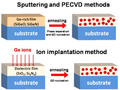
In the third chapter is presented a detailed experimental investigation on the synthesis, structural characterization and optical absorption properties of ensembles of Ge quantum dots (QDs) embedded in a dielectric matrix. Ge QDs embedded in SiO2 or Si3N4 matrices have been synthesized through thermal annealing of Ge-rich films deposited by plasma
37
enhanced chemical vapour deposition (PECVD), co-sputtering deposition or Ge implantation technique. We will demonstrate that the type and stoichiometric quality of the hosting matrix has a fundamental role in controlling both the growth and the optical properties of Ge QDs. In particular, the optical properties of these systems appear to be quite complex and not always can be described only by their size through quantum confinement effects. For this reason, we studied the contributions coming from other structural parameters such as: QD density and spacing, distribution, hosting matrix and amount of defects. We will give evidence that such parameters have a strong role in the light absorption process of Ge QDs and clearly affect both the bandgap and the optical oscillator strength of these systems with respect to a pure quantum confinement regime.
The fourth chapter is devoted to the investigation of the conduction mechanism and photo-carrier extraction efficiency of prototypal devices using Ge nanostructures. We will demonstrate that Ge nanostructures can be effectively used as active absorber and conductive medium in light harvesting devices. In particular, we will report on the spectral response of metal-insulating-semiconductor (MIS) devices employing single amorphous Ge QW or packed arrays of Ge QDs as active photo-conductive medium. Devices with Ge QWs exhibit a clear enhancement of the photocurrent with the QW thickness, indicating a key role of Ge in the electron-hole pair generation. When Ge QDs are used even larger performances are achieved due to a large photoconductive gain mechanism activated by the presence of Ge QDs. We will investigate the role of Ge QDs in the performances of these type of photodetectors and explain such a large photoresponse as the result of a photoconductive gain mechanism assisted by trapping of photo-generated holes in Ge QDs. These results clearly demonstrate the large applicability of Ge QDs for the fabrication of high-efficiency and fast Si-compatible photodetectors and their potential application as active light-sensitizer medium in future PV cells.
Chapter 2
Light Absorption at the nanoscale: the ideal case of
Ge quantum well
In this chapter, we will give a brief overview of the theory of the light absorption in bulk semiconductor and NS materials. In particular, we will provide more details on the Tauc approach theory, used to evaluate the optical properties of bulk amorphous materials (such as bandgap, DOS, optical oscillator strength) from absorption spectroscopy measurements and the validity of this method also in describing amorphous NS. Then, we will investigate the optical absorption of single amorphous Ge quantum wells (QWs, 2 to 30 nm thick) deposited at room temperature on fused silica substrate. As the result of the confinement of this system, the optical absorption shows a marked size-dependent blue-shift and an enhanced oscillator strength with reducing the QW thickness. Such a behavior is sign of a strong quantum confinement of excitons occurring at room temperature and for a disordered material as amorphous Ge QW is. Still, the optical bandgap and the oscillator strength, extracted by Tauc method, are fully in agreement with the theoretical values calculated within the effective mass approximation (EMA), confirming the validity and the effectiveness of our approach based on optical absorption spectroscopy.