Academic year 2014/2015 Session I ( July 2017)
ALMA MATER STUDIORUM - UNIVERSITÀ DI BOLOGNA
SCHOOL OF ENGINEERING AND ARCHITECTURE
Department of Electrical and Information Engineering of Energy "Guglielmo
Marconi” (DEI)
MASTER THESIS IN
ADVANCED ELECTROMAGNETIC TRANSMISSION TECHNIQUES AND DEVICES
Time-Modulated Array Co-Simulation with the Aid of
Commercial Software
Candidate:
Supervisor:
ii
internationally---iii
ACKNOWLEDGEMENTS
I would like to start thanking to people who, from the working point of view, have accompanied me along this path. First of all, a sincere regards to Professor Diego Masotti, for allowing me to make this experience of thesis. You are one of most beloved, intellectual and helpful Professor in Department of Electrical, Electronic, and Information Engineering at University of Bologna. Thank you for all the things that you taught me from the technical side with full passion of energies. But especially for having revived me the urge to search for this scientific field. I would take this opportunity to thank PhD fellow Marco Fantuzzi whose help, guidance, company and support gave me moments that I cannot forget. He made this journey more exciting and it would have been impossible without his technical expertise.
I would specially like to mention my alumni senior and dear brother Rafaqat Ali whose
continuous support has been always there from the very first day I planned to come to Bologna. Rafaqat! I am fortunate to have a person like you in my life.
Now I would like to thanks, those people who accompany me in life, my friends Usman, Guido, Abdullah, Sana, Eliana, Subhan, Andrea, Farrukh, Faiq and all others. With you guys I shared some best moments of my life. Wherever life and work will bring, therewill always a pleasure for me to spend time together with you guys.
I am grateful to my parents, Mr. Muhammad Ahsan and Mrs. Almas Ahsan, for all their prayers and for giving me the gifts of life and education. I couldn’t have reached what I have achieved in life without their sacrifices. I can never forget they instilled in me values of conviction,
persistence, and hard work. They have always been a source of inspiration and courage for me and I can never thank them or repay them enough for the virtues they have given me.
Finally big thanks to my sister Tooba and brothers Haris, Haseeb for appreciation and all kind of support throughout my academic career. Thank you again and I love you all.
iv
TABLE OF CONTENTS
Abstract
……… viChapter 1. Time Modulated Array
1.1. Introduction ……… 11.2. TMA for Wireless Power Network ……….. 3
• TMA Radiation at Fundamental Frequency and Sideband ……… 3
Chapter 2. Explanation & Simulation of TMA with Commercial
Software
2.1. Advanced Design System ……….………… 6• Key Features ……….…….. 7
• Specifications ……….……... 7
• Advanced Design System Users ..………. 8
• Environment ……….. 9 • Main Window ……….…… 9 • WorkSpace Views ……… 10 • Design Views ……….. 10 • Schematic View ……… 10 • Symbol View ……… 12 • Layout View ………. 12
• Data Display Window ……… 13
• Exiting From ADS ……….. 14
• Using Design ………. 15
• Creating a New Schematic ……….. 15
• Creating a New Layout ……….. 16
• Creating a New Symbol ………. 17
• Momentum ……… 17
• Setting and EM Simulation ……….. 18
• Ports and References Planes ………. 19
• Meshes ……….. 21
• Simulation and Data ………. 23
v 2.2 Envelope Simulation with ADS and Software Limitation
• Brief Explanation ………. 26
• Accurate Co-Simulation Method of Coupled Non-Linear/Electromagnetic System ………. 28
2.3 ADS Harmonic Balance Inter-Modulation Analysis • Non-Linear and Full Wave Co-Simulation ………. 37
• Detailed Theory of Wireless Power Transfer Approach in Two-Step ……… 37
• Localization Step-1 ………. 44
• Power Transfer Step-2 ………. 45
vi
Abstract
This thesis report exhibits an integrated Electromagnetic/Circuit level technique to analyze the time modulated arrays. I restate this work in commercial software which was already
developed in CAD domain i.e. combining the exact harmonic balanced based analysis of non-linear switches with the electromagnetic characterization of the radiating elements. In this commercial software I try to perform a full-wave co-simulation to compute the radiated far-field envelope to show the array behavior. Simulation in this new software allows a precise evaluation of several non-linear performance aspects of the radiating system, such as power usage capabilities and the switch modulation frequency boundary.
Secondly I also discuss a TMA wireless power transfer technique which is based on two step procedure. In this case I carry out the full wave co-simulation in this new commercial software to analyze the antenna array with modulated non-linear feeding network. Schottky-diode based network provide proper modulated RF excitations of the array elements. Therefore, the array architecture is extremely simple, if compared to phased arrays, only simple control circuit board.
- 1 -
1. Time Modulated Array
1.1
Introduction
The wireless domain that requires mounting mobility, capacity and robustness have enhanced wireless communications as the most efficient, progressive sector of the telecommunication industry nowadays. As a result, the increasingly limited wireless medium has to be efficiently utilized. In doing so, antennas are used. Antennas play a significant role in achieving the development. A proper modification and enhancement of features of the antenna and sound signal processing allow us to act in the space, frequency efficiently, and time domains to bestow a viable option to the complex task of realistically addressing the required signals. It also helps to mitigate the unwanted ones.
The research centered on the development of new technologies allows for reduced power consumption of sensor networks. It aims at the elaboration of smart antennas with low loss of power, muting, and adaptive beamforming features. Besides this, a smart antenna technology has to take into account the hardware complexity, making the solution feasible in the context of sensors. Moreover, antenna devices development to suit the needs of sensor networks must be efficient enough to sense the external electromagnetic environment, thus appropriately reconfiguring the radiation characteristics of the generated field. It will assure both the necessary quality of service of the communication link and reduced power consumption. This chapter demonstrates the use of time modulation as new statistics in the design of ultra-low side-lobe level arrays. This solution offers less tolerance errors with respect to conventional tapered amplitude excitations, but suffers from the existence of unwanted radiation in
correspondence of sideband signals spaced at multiples of the modulation frequency. Various solutions exhibit the feasibility of time-modulated arrays featuring both side-lobe reduction and sideband suppression by exploiting the design parameters offered by the switch modulation laws. Anyway, more recently, sideband radiation of TMAs has demonstrated to be a deployable additional feature of these radiating systems, as will be better described in next section. An important improvement in time-modulated arrays (TMA) performance comes out from the removal of the common start time condition for the switches and the introduction of different switching strategies in which the element “switch-on” times can be arbitrary [2]. In one of these approaches the switch modulation period is divided into elementary time intervals of the same duration and a binary genetic algorithm is used to select the ENABLE-DISABLE states of the switches.
Some extent infinite control sequence combinations together with the ease of putting into use make the TMA a multifaceted and adequate radiation system for contemporary wireless
- 2 -
applications. The real-time reconfigurability of the radiation pattern designates the TMA as the best possible prospect for software-defined radio solutions.
Although, the conveniently accessible design approaches fundamentally make use of isotropic radiators and invariably presume ideal switches in the optimization process, it causes a
noteworthy loss of information regarding the physical reality. Mainly, the aspects that cannot be considered encompass of the actual antenna radiation pattern and possible electromagnetic interactions along with the feeding network. It also includes the nonlinear behavior of the switching devices and lastly the intrinsic dynamics of the radiation mechanism.
The goal of this thesis work is to provide a rigorous design approach to TMAs by means of available commercial softwares.
However, various technical problems continue to exist to develop the necessary antenna technologies which have the potential to support the features mentioned above in a contained physical space that the mobility demand domineers. As a matter of fact, modern wireless merits contemplate the multiple-antenna techniques to utilize space variation, spatial multiplexing, and beamforming to attain excellent standards. It is done to enhance reliability and increase the capacity. Such a useful framework is achieved at the cost of several system complexities. They may be unaffordablein small-size and low-cost sensor appliances and devices with the necessary low power utilization.
The idea of TMA is a feasible multi-antenna method that provides an important hardware to
make less complex [2]. Furthermore, TMA, represent as unconventional phased arrays architectures, have been intensively researched during the previous years at a rising rate.
- 3 -
1.2. TMA Wireless Power Transfer
In this chapter, a smart wireless power transmission technique is discussed which is based on a 2-step procedure to exploit real-time beaming of TMA. In this case the drawback of sideband radiation of these radiating systems favorably used for on purpose wireless power transfer (WPT).
In the first step to accurately localize the tag to be powered and in the second one to perform directive WPT [1]. The approach is first theoretically discussed, and then the numerical
procedure, which integrates full-wave analysis of the antenna array with nonlinear simulation of the modulated nonlinear feeding network, is used to validate the principle of operation and to include nonlinearities and electromagnetic couplings affecting the whole system
performance.
The procedure allows a flexible design of the time-modulated- array-based WPT system, taking into account the impact of array elements layout and spacing on localization and power
transmission performance.
Simulation of the first step is carried at 2.45 GHz, with a Schottky-diode-based network to provide proper modulated RF excitations of the array elements.
TMA radiation at Fundamental and Sideband frequencies
Non-linear switches are driven by periodical control sequence at TMA elements ports which leads to nearly infinite number of excitation combinations, not only the switch on percentage but also the rise and fall instants. In this case optimization procedure can be adapted to manipulate an extreme versatility of these radiating systems. Figure 1.1 shows very simple architecture for a standard linear array [1].
Figure.1.1 Schematic illustration of a linear 𝑛𝐴-element TMA with comprehensive diodes switch bias networks, with dc-block
- 4 -
This is an extremely simple array architecture, like if compared to the phase arrays. There isn’t required complex phase shifter but control boards only which is simple. Furthermore, TMA additionally offers known capability which is not feasible for other radiating architecture represented by a multi-frequency radiation mechanism and the focus of this chapter will represent this.
Let’s start to consider a linear array whose nA elements are resonant at fundamental
frequency f0 and along the direction â(â. r̂ = cosφ) are aligned with L spacing inter-element
[1]. At the ith antenna port is the RF switch driven by a sequence which is periodical rectangular pulses of period T=1 f⁄ and UM i(t) normalized amplitude which leads to replaced the constant
excitation coefficient Ai with time-dependent version Ai Ui(t). In this way the whole array radiated far-field becomes time dependent as well. This time dependency of the array factor AF as breakdown in the following field evaluation in the point ((r, θ, ∅):
1.1
Where the free-space phase constant is β, and E0 represents the radiated far-field at the carrier frequency f0 radiated by the base element of the array. Because of periodicity the control
switch sequence is possible to Fourier transform the time dependent array factor.
1.2 Where Uhi is the hth Fourier coefficient of the Ui(t) pulse.
Definitely, at the fundamental frequency f0(h=0) the TMA is able to radiate but this happens also at sideband harmonics f0± hfM(h=±1, ±2..). This sideband radiation (SBR) is efficiently
received/transmitted due to the modulation frequency fMwhich is low value with respect to the
- 5 -
In the start of TMA’s usage, the phenomenon of sideband radiation (SBR) has represented an unwanted radiation. In this chapter there are multiple efforts taken into account to suppress this power wastage. In fact, we intend to exploit the capabilities of direction finding and harmonic beaming to realize a new and smart WPT procedure strategy.
In second chapter there is a detailed explanation of the procedure and also the simulation results taken from commercial software.
- 6 -
Chapter 2. Simulation of Time Modulated Array with Commercial
Software
This chapter primarily examines active microwave circuit design, an important part of microwave engineering. This subject has worldwide appeal given the incredible growth in mobile and satellite communications. In the past, the use of microwaves was limited to radars and weapon systems, and to remote sensing and relay systems. However, due to the rapid expansion of mobile and satellite communication systems in recent years, systems that use radio waves or microwaves can be found in almost every sphere of our lives. The design environment for active microwave circuits has changed drastically with the continuous
expansion of microwave applications into our daily lives. Recently, a variety of software design tools applicable to circuit design, system design, and electromagnetic analysis of passive structures has emerged. This has significantly reduced the need for analytical methods and specific design-oriented, in-house programs for the design of circuits and systems. With these advances, the rapid exchange of results between designers has facilitated independent study and experimentation with basic concepts using software tools and practical designs. Clearly, innovations in the field underscore the necessity for advanced education in active microwave circuit design and improvements to relevant software tools.
The popular Advanced Design System (ADS) from Agilent Technologies is the design tool used in the chapter as it has the longest proven track record compared to other design software. However, since most features of ADS are also available in other, similar design software, I believe that selecting ADS as the design tool will not present any critical limitations.
Previously we were using old design software at University of Bologna for the simulation which has high performance, even compared to commercial ones, but lacks in nonlinear device libraries, The purpose of my thesis job is to introduce the new software in university that has vast features and built-in powerful tools and plenty of library devices which we can perform full scale-simulation efficiently, especially a nonlinear/electromagnetic co-simulation for TMA analysis.
2.1. Advanced Design System
“Advance Design System” is the world’s leading electronic design automation software for RF, microwave, and high speed digital applications. In a powerful and easy-to-use interface, ADS pioneers the most innovative and commercially successful technologies, such as X-parameters*
- 7 -
and 3D EM simulators, used by leading companies in the wireless communication & networking and aerospace & defense industries [3]. For WiMAX™, LTE, multi-gigabit per second data links, radar, & satellite applications, ADS provides full, standards-based design and verification with Wireless Libraries and circuit-system-EM co-simulation in an integrated platform.
While the Key Benefits of ADS are:
• Complete, integrated set of fast, accurate and easy-to-use system, circuit & EM simulators enable first-pass design success in a complete desktop flow.
• Application-specific Design Guides encapsulate years of expertise in an easy-to-use interface.
• ADS is supported exclusively or months earlier than others by leading industry and foundry partners.
Advanced Design System (ADS) continues to lead the RF EDA industry with the most innovative and commercially successful technologies, including Harmonic Balance, Circuit Envelope, Transient Convolution, Keysight Ptolemy, X-parameter*, Momentum and 3D EM simulators (including both FEM and FDTD solvers). With ADS’s Wireless Libraries and circuit-system-EM co-simulation technology, ADS provides full, standards-based design and verification within a single, integrated platform.
Key Features & Specifications:
ADS Core is the starting element to build up your design and simulation capabilities. It already contains powerful features [3].
• Project design environment to input schematics, launch simulations and manage design projects
• Data display to manipulate and plot data
• Linear simulator for S-parameters, DC and small signal AC analysis • RF system simulator
• Additional model libraries- RF system, RF passive and multilayer interconnects • Passive circuit design guide to synthesize matching networks and passive functions
- 8 -
Advanced Design System Users
There are different users who can use as per their requirement which are mentioned below [3]: • MMIC Designers
• Signal Integrity Engineers • RFIC Designers
• RF & Microwave Board Designers
• RF System-in-Package & RF Module Designers • Power Electronics Designers
In this chapter we worked as a RF & Microwave Board Designers. Ever increasing substrate layer counts, smaller form factors, complex packaging technologies, and closer design proximity continue to make RF/MW board designs ever more challenging. ADS provides integrated
system, circuit, and EM simulators, layout, and powerful optimizers to help increase
productivity and efficiency, validating high-yield designs prior to manufacturing. ADS works with framework integration products, such as Mentor and Cadence, to fit in your design flow. For general information on Keysight's solutions, refer to RF & Microwave Board Design.
Key Success Factors for RF Board Design Flows
The keys to success in creating an efficient, practical RF Board design flow include:
• The Widest variety of synthesis capabilities that enable RF Board designers to explore alternatives quickly and balance RF performance, parts count, and board area, within seconds, as well as to assess the cost-effectiveness of whether to make or buy a commercial component.
• Accurate model libraries that support different simulation domains for various
applications. Behavioral models are also important for initial system level designs and they can be extracted from datasheet, measurement, or simulation based.
• Comprehensive vendor supplied libraries that enable the simulation of off-the-shelf components.
• Accurate RF/microwave physical models such as microstrip, stripline, and coplanar waveguide.
• Comprehensive simulation technologies in one environment including linear/nonlinear in frequency and time domain
- 9 -
ADS Design Environment
This section describes the ADS Design Environment. ADS Main Window
The ADS Main window (also referred to as Main window) is your first interface to start using the ADS. It helps you to access all the features supported by ADS [3]. It allows you to:
• Create and manage a workspace. For more information, refer to Workspace. • Organize design data in virtual folders.
• Open design view(s) and data display window.
• Perform design flow settings. For more information, refer to Design Flow Settings. • Set program preferences. For more information, refer to Setting Preferences for
Miscellaneous Options.
• Change toolbar configuration and keyboard shortcuts (Tools > Hot Key/Toolbar Configuration)
• Manage technology associated with a workspace. For more information, refer to Technologies.
• Record and play macro. For more information, refer to Playing an AEL Macro.
• Load AEL files/commands from the Command line. For more information, refer to Command Line.
• Launch the text editor. For more information, refer to Using the Text Editor. • Show/Hide all windows.
• Index large workspaces.
• Convert projects (created using ADS 2009 Update 1 or earlier versions) to a workspace. For more information, refer to Converting Projects to Workspaces.
• Access examples that ship with ADS. For list of examples that are shipped with ADS, refer to Examples.
- 10 -
Workspace Views
The following table describes the workspace view options [3].
Design Views
You can create schematic, symbol, and layout design views. A design can consist of a number of schematics and layouts embedded as subnetworks within a single design. Views allow you to modify the schematic, layout and symbol independently.
You can create multiple views to control simulations and track design revisions. Layout and schematic toolbars have been reconfigured to various smaller toolbars. This enables you to personalize ADS to your needs. For information on reconfigured toolbars, see Layout and Schematic Toolbars.
New and improved Layout and schematic hotkeys. There are now single-key hotkeys for various common operations such as M for move. For information on list of hotkeys, see Layout
Hotkeys.
Schematic View
In schematic view you can create designs:
• By placing components, pins, data items, units, variables, and equations.
• Using a template. You can also save your design as template. For more information on templates, see Simulation Templates.
• Using the Schematic Wizard that helps you prepare the design for simulation. For more information, see Schematic Wizard.
- 11 - • The Title bar displays the window type, design type, filename, and a number identifying the
type of window.
• The Menu bar displays the menus available in that window.
• The Toolbar contains buttons for frequently used commands and for choosing the appropriate orientation for components. The collection of buttons on the toolbar is
configurable (Tools > Hot Key/Toolbar Configuration) and can be toggled on and off (View > Toolbar).
• The Palette List enables you to choose a category of components to place on the Component Palette.
• The Component History drop-down list is continuously updated to reflect the components you have placed in your design. It provides a quick method of placing another instance of a component in your design and can be used as a starting point for creating a custom palette. • The Drawing area is where you create your designs.
• The Component Palette contains buttons for placing components.
• The Prompt panel provides messages to assist you during the execution of most commands, as well as various pieces of information to assist you in creating a design.
• The Pop-up menu enables you to access many common commands with a minimum of mouse movement. You access the pop-up menu by pressing the right mouse button in the drawing area of any design window. The context-sensitive commands appear on the pop-up menu when the pointer is positioned over certain shapes or text and on right click.
- 12 -
Symbol View
To create a new Symbol, follow the steps below [3]:
1. Start ADS and open an existing workspace or create a new workspace.
2. From the main ADS Window, use any of the three options to open the New Symbol dialog box:
▪ Select File > New > Symbol.
▪ Click New Symbol button ( )from the toolbar.
▪ Right click on the workspace name and select New Symbol option.
From the Library drop-down list, select the library name where the new Symbol will be stored.
Enter the new cell name or click the Browse Cells button to select cell from the existing cells of the selected library.
Click Edit View Name to create a new symbol view with the default name, i.e., Symbol or a new view name in View Name Editor window.
Click OK to open the symbol window where you create a Symbol View. The following figure displays the Symbol view.
Layout View
To create a new Layout, follow the steps below [3]:
1. Start ADS and open an existing workspace or create a new workspace.
2. From the main ADS Window, use either of the three options to open the New Layout dialog box:
- 13 -
▪ Select File > New > Layout.
▪ Click New Layout button ( )from the toolbar.
▪ Right click on the workspace name and select New Layout option.
From the Library drop-down list, select the library name where the new layout will be stored.
Enter the cell name or click the Browse Cells button to select cell from the existing cells of the selected library.
Click Edit View Name to create a new layout view with the default name, i.e., Layout or a new view name in View Name Editor window.
Click OK and the layout window opens where you create the Layout View. The following figure displays the Layout view.
Data Display Window
The Data Display window allows you to [3]:
• View and analyze the data generated by simulation, as well as that has been imported from other sources, such as a network analyzer or CITIfile.
• Display data in a variety of plots and formats. • Create plots with more than two axes.
• Add markers to traces to read specific data points.
• Write mathematical equations to perform complex operations on data, and display the results.
- 14 -
• Edit plot titles and axis labels, equations, text, drawing objects, and column headings in lists. The following figure displays the Data Display window.
Exiting from ADS
To exit the ADS program from the Main window or any of the design windows, perform the following [3]:
1. Select File > Exit from the Main window or
Select File > Exit Advance Design System from any design window (such as Symbol, Schematic, or Layout).
The Save Modified Designs window is displayed. 2. Click Yes to save and exit.
- 15 -
Using Designs
ADS allows you to create various designs such as, schematic, symbol, and layout [3]. A design can consist of one or more schematics and layouts embedded as subnetworks within a single design. All designs in a workspace can be displayed and opened directly from the ADS Main window. The designs are stored in a cell.
An ADS design window is used to [3]: • Create and modify circuits and layouts. • Add variables and equations.
• Place and configure components, shapes, and simulation controllers. • Specify layer and display preferences.
• Include annotations using text and illustrations.
• Generate layouts from schematics (and schematics from layouts).
Creating a New Schematic
Following are the steps to create a new Schematic:
1. Open an existing workspace, or create a new workspace.
2. Select File > New > Schematic from the ADS Main window, to open the New Schematic dialog box.
3. From the Library drop-down list, select the library name where the new schematic is stored. 4. Enter the new cell name or click Browse Cellsto select the cell from existing cells of the
selected library.
By default, a view is created in a new cell. To add it to an existing cell, change the cell name or as a shortcut, instead of using File > New > Schematic. You can right-click on an existing cell in the Folder View or Library View and select New
- 16 -
5. Click Edit View Name to create a new view.
6. Select the template from Schematic Design Templates list, or check the Enable the Schematic Wizard to start the Schematic Wizard.
7. Click OK.
The new schematic window is displayed.
Creating a New Layout
To create a new Layout, follow the steps below:
1. Start ADS and open an existing workspace, or create a new workspace.
2. From the ADS Main window, select File > New > Layout to open New Layout dialog.
1. From the Library drop-down list, select the library name where the new layout is stored. 2. Enter the new cell name or click the Browse Cells button to select cell from the existing cells
of the selected library.
3. Click Edit View Name to create a new view.
4. Click Change to change the connectivity mode for the new layout. For detail information, see Connectivity Modes.
- 17 -
Creating a New Symbol
To create a new Symbol, follow the steps below:
1. Open an existing workspace, or create a new workspace.
2. Select File > New > Symbol from the ADS Main window, to open the New Symbol dialog box.
3. From the Library drop-down list, select the library name where new symbol is stored. 4. Enter the new cell name or click Browse Cells to select cell from the existing cells of the
selected library.
5. Click Edit View Name to create a new view. 6. Click OK.
The new symbol window is displayed.
Momentum
To calculate passive structures and antenna, methods based on electromagnetic theory have been developed in the past and are still being studied but the method of calculation varies considerably depending on the structures.
The structure analysis that uses Maxwell equations for electromagnetics is known as EM simulation (electromagnetic simulation). The EM-simulation tool for a planar structure is built into ADS and is called Momentum.
- 18 -
Settings and EM Simulation
Substrate and Layout LayersMomentum provides electromagnetic solutions for a planar structure (a vertically uniform dielectric structure), the substrate structure (the vertical structure) composed of multiple substrate layers must first be specified. Also, users should map multiple metallization layers on the substrate layers. For the specified substrate and metallization structures, Momentum calculates the Green’s functioned and stores it for calculation efficiency.
Figure 2.1 shows a window for determining the substrate structure[4]. On the menu bar of the ADS Layout window, select Momentum > Substrate > Create/Modify to display the window shown in Figure 2.2. The Substrate Layers tab in the figure defines the structure of the substrate. The dielectric structure in this example consists of FreeSpace, Alumina, and GND. When multilayers are required, a new substrate layer can be added by clicking Add; layers can also be deleted by clicking Cut. The boundary conditions for FreeSpace are the same as the properties in free space. FreeSpace can be set to a shielded structure, where a conductor plate is placed at the ceiling. By clicking the layers in the dielectric structure, its parameters can be modified. For example, click the dielectric layer Alumina and activate the window that defines the attributes of that dielectric layer. The Dielectric Thickness and Substrate Layer Name can be specified. The specifications for each layer are completed by entering the Thickness, Dielectric
Permittivity, and Dielectric Loss Tangent information for each dielectric. Its permittivity Er and
permeability Mu can be defined in a variety of formats. The permittivity and permeability are defined in terms of the general Re, Loss Tangent form and it is also possible to define them in other ways.
Figure 2.1 Substrate Layer tab window
Next, the location of the metallization must be specified for the calculation of the Green’s function, which is done by opening the Layout Layers tab and specifying the metallization on which the substrate layer is located. The window for the Layout Layers tab is shown in figure 3.
- 19 - Figure 2.2 Layout Layers tab window
This process is absolutely necessary if you do not want to use the substrate provided in ADS, but intend to enter the substrate information directly. Once specified as described above, the Green’s function required to perform the simulation can be computed. To do this, click
Momentum > Substrate > Precompute Substrate Function. This computes the Green’s function
for the desired frequency range and, because the Green’s function will be used repeatedly, it does not matter even if the calculation is done for a wider frequency range.
Ports and Reference Planes
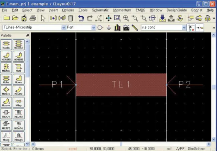
Figure 2.3 is a conductor shape drawn on the layer named cond[4]. A microstrip line having a 25-mil width and 100-mil length is inserted on the substrate shown in Figure 2.1 and 2.2. The microstrip line is drawn first as a circuit in the Schematic window; the drawing is generated using the Layout > Generate/Update Layout commands on the menu bar of the Schematic window.
- 20 -
The input and output ports must be set up in order to perform Momentum simulations. To this end, the layer where the ports are connected must be specified as the inserting layer.
Afterselecting the cond layer as the inserting layer, the ports can be attached by clicking the icon. Then, the drawn shape appears, as shown in Figure 2.4[4].
Figure.2.4. The drawing after the ports are inserted
To set the parameters of the port, select Momentum > Ports > Editor on the menu bar. Click the port to display the Port Properties Editor window shown in Figure 2.5. Port modes include
Single, Internal, Differential, Coplanar, Common, and Ground Reference. A Single Mode port is
assigned by default, which can be widely used for a general microstrip-structure simulation. The port impedance can be set in the Impedance field and it can be set to a complex value using the
Real and Imaginary fields. The port impedances become the reference impedances for the
S-parameters. Reference Offset moves the reference line of the computed S-S-parameters. It is used to remove the effect of the length of the microstrip lines. When the Port Properties Editor settings are completed, new perpendicular lines are created that indicate the position of the reference plane.
Figure 2.6. Shows the window after completing the port setup[4]. The reference lines can be moved by entering the Reference Offset parameter in the Port Properties Editor window and can also be moved using the mouse by selecting the reference line and dragging it.
- 21 -
Figure 2.5. Port Properties Editor window
Figure 2.6. The window after completing the Port Properties Editor settings
Meshes
When the work to complete the port setup is finished, the electromagnetic problem setup of a structure is completed. Therefore, after creating a mesh in Momentum, the previously
described matrix Equation is generated and solved. Even when a user does not specify the mesh, Momentum automatically generates the mesh after which the calculation is performed; however, the user can adjust the generation parameters of the mesh [4].
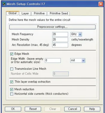
The Mesh Frequency is set in the Global tab of the Mesh Setup Controls window. The Mesh
Frequency field determines the reference frequency for mesh generation and is normally set to
the highest frequency of simulation. The Mesh Density field determines the cells per unit wavelength. In the case of a circuit that is 3-wavelengths long, setting the Mesh Density to 20 will create a total of 60 cells. A dense mesh is required in the case of complex structures, while
- 22 -
the default mesh value is adequate for simple circuits such as microstrips. The curve portions of the circuit are divided into triangular meshes. The Arc Resolution field determines the angle of triangular meshes and can be set up to a maximum of 45°. The smaller the angle, the more exact the analysis, but smaller angles should be avoided because they make processing time too long. The Transmission Line Mesh field defines the number of mesh per unit width of a microstrip line, and is disabled by default. Usually, the remaining entries use the given default values.
The conductor surface specified for Momentum calculations is divided into triangular or rectangular meshes. To set the mesh parameters, click Momentum > Mesh > Setup and the Mesh Setup Controls window shown in Figure 2.7 appears.
Figure 2.7. Mesh Setup Controls window
After the mesh setting is finished, the meshes can be shown in advance by clicking Momentum > Mesh > Preview; then, the highest frequency of the simulation frequency range, (20 GHz as shown in 2.7 is entered. Click OK and the layout window will display the mesh, as shown in 2.8.[4]
- 23 -
Figure 2.8. Microstrip lines are divided by mesh
Simulation and Data
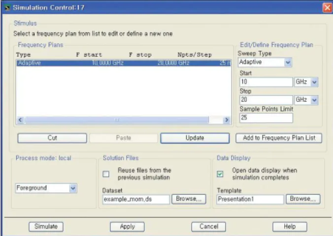
Now the settings for Momentum simulation are completed. For the simulation, when you select
Momentum > Simulation > S-parameters, the window shown in Figure 2.8 appears [4].
Figure 2.9. Simulation Control window
Simulation frequencies can be selected using the Edit/Define Frequency Plan in the top-right corner of the window shown in Figure 2.9 [4]. Four types of frequency selections are provided:
Adaptive, Logarithmic, Linear and Single Point. Adaptive simulation frequencies are computed
by adaptive algorithm. Since the S-parameters of the given frequency range can be obtained by interpolating a small number of S-parameter samples, the algorithm determines the simulation frequencies so as to eliminate the uncertainty of the interpolated S-parameters. The Adaptive method is used because Momentum simulation requires a long computation time. The Sample
Points Limit field specifies the maximum number of samples. The Logarithmic selection sets the
- 24 -
start and stop frequencies, and the numbers per decade. The Linear selection sets the simulation frequencies linearly to increase from the start to the stop frequencies. The Single Point selection is the simulation for one frequency.
The calculation results are stored as a dataset in the directory data. A user can identify the dataset by entering its name in the Dataset field; the default name is layout name_mom. There is a check box for whether or not previously simulated data will be reused; this, however, is usually not selected by default. In Figure 2.9, since Open data display when simulation
completes is checked, the display window is opened automatically after simulation. The
simulation frequency range is set to 10–20 GHz and the Sweep Type in Figure 2.9 is set to
Adaptive and Sample Points Limit is set to 25.
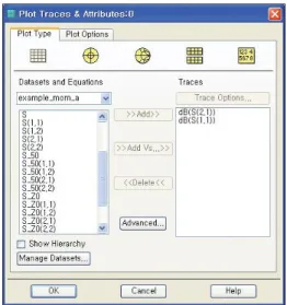
When the simulation is finished, the display window will automatically open due to the
selection of that option in Figure 9. In order to view the results, click the icon Rectangular plot in the display window. The Plot Traces & Attributes window in Figure 10 opens and it will contain the computed parameters shown in Figure 2.10. The S here represents the
S-parameters normalized by the port impedances set by the Port Properties Editor during Momentum set up. The port impedances were set to 50 Ω. S_50 represents the S-parameters normalized by 50 Ω. Therefore, S_50 and S are the same S-parameters in this case. However, if the port impedances set by the Port Properties Editor are different, the two are different S-parameters. Similarly S_Z0 represents the S-parameters normalized by impedance Z0. Momentum first solves the port impedances and propagation constants based on the cross-sectional shape of the ports, as explained previously. The results are stored in Z0 and Gamma, where Z0 represents the characteristic impedance and Gamma represents the propagation constant of the ports. Thus, S_Z0 represents the S-parameters normalized by impedance Z0 that is determined by Momentum.
- 25 -
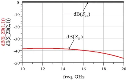
Figures 2.11 and 2.12 show S and S_Z0 [4]. The previously defined 100-mil-long by 25-mil-wide microstrip line has a characteristic impedance of approximately 29.3 Ω and an electrical length of 82° at 10 GHz when computed using LineCalc. The Momentum calculation results of Z0 show a 29.7-Ω characteristic impedance that is close to that of the LineCalc computation. The
impedance Z0 is used as a reference impedance for the normalized S-parameters S_Z0. Since the analyzed structure is a simple microstrip line, S_Z0 will show the small insertion loss with respect to frequency. This is shown in Figure 2.12, while the S-parameters shown in Figure 2.11 exhibit a significant insertion loss and return loss due to mismatch.
Figure 2.11. Momentum simulation results. The parameters represented by S in the dataset are the
S-parameters with the reference impedances specified by the Port Properties Editor.
Figure 2.12. S_Z0 results. The S_Z0 represents the S-parameters with the reference impedances Z0, which
represents the port impedances computed in the Momentum simulation.
However, in Figure 2.12 the return loss still shows an approximate value of –40 dB [4], which should be infinity. The exact reason for this is unknown, but may be due to dispersion in the microstrip line and cross-coupling of the port.
- 26 -
Summary
• The simulation in ADS is performed in the ADS Schematic/Layout window and the work in this window is saved in the network directory of the working project. The simulated data is saved in the data directory of the working project. The data can be viewed in the display window and the display window data is saved in the working project directory.
• Circuit simulations can be generally classified into DC, transient, AC, and harmonic balance. The S-parameter simulation is a kind of AC simulation.
• Layout is classified into two types, manual layout and auto layout. The layers, grid, and components are the basic design concepts in drawing a layout.
• Momentum is the tool for EM solving of a planar structure. The substrate structure, layer metallization, and assignment of ports are necessary for EM simulation of a planar structure. • After the Momentum simulation, the S-parameters S, S_50, S_Z0 appear in the dataset and their physical meanings are explained. Also, port data Z0 and Gamma appear in the dataset and they represent the port impedances and propagation constants, respectively.
2.2 Envelope Simulation with ADS and software Limitation
Brief Explanation
Modulation-Oriented piecewise Harmonic-balance theory describes that the entire circuit/system is split into two sub networks, a linear explained concerning the frequency domain, and a nonlinear explained regarding the time-domain. The two sub-networks are connected using number (𝑛𝐷) of standard (or device) ports. It is where the Kirchhoff current
laws are applicable in the frequency domain. It is done to build the nonlinear solving system. In the given scenario, the linear portion contains radiating elements, too. A precise description of the linear sub-network is attained by resorting to full-wave numerical solvers; it is the typical case for high-frequency or compact microwave circuits or both.
From a circuit-level viewpoint, the presence of a radiating antenna requires the system output to be described regarding radiated field instead of standard circuit network operations. This calculation can be composed forthrightly as the antenna is a linear component. As an example, let us consider a steady-state regime under sinusoidal excitation, which is described by a set
- 27 -
𝑛𝐻of harmonics of the fundamental (angular) frequency. The 𝑛𝐴-dimensional vector of the
excitation currents at the feeding points of the 𝑛𝐴monopoles can be represented in the form;
𝑖𝐴(𝑡) = 𝑅𝑒[∑ 𝐼𝐴,𝐾
𝑛𝐻
𝑘=1
exp(𝑗𝑘𝜔0𝑡)]
Let us now establish a spherical coordinate system (r, θ, ∅ ) , with origin in the phase center of the antenna array. The far field radiated by the array at the fundamental frequency ( k= 1) may be cast in the form
𝐸(𝑟, 𝜃, ∅ ; 𝜔0) = exp (−𝑗𝛽𝑟) 𝑟 ∑[𝜃̂𝐴𝜃 (𝑖) 𝑛𝐴 𝑖=1 ( 𝜃, 𝜑 ; 𝜔0) + ∅̂𝐴∅(𝑖)( 𝜃, 𝜑 ; 𝜔0)] 𝐼𝐴,1 (𝑖) 2.2
Where 𝜃̂, ∅̂ are unit vectors in the directions of θ,∅, respectively, and the scalar components are 𝐴𝜃(𝑖), 𝐴∅(𝑖)of the normalized field. EM simulation generated these components with only the excited 𝑖th monopole by a sinusoidal unit-current source of angular frequency 𝑤0. If the non
linear radiating system operates under modulated RF-drive the electrical regime is described as being dependent on 2 uncorrelated time variables which are known as 𝑡𝑀 a slow envelope and
𝑡 as a fast carrier time. According to the envelope analysis approach, the vector of eqn (2.1) representing the currents at the antenna feeding points is replaced by
2.3
That’s the constant 𝑘th phasor 𝐼𝐴,𝐾 of eqn-2.1 is replaced by the 𝑘thenvelope time dependent
phasor 𝐼𝐴,𝐾(𝑡𝑀). Sequentially the time-dependent modulation laws may explicitly formulated as
2.4
Where 𝑤𝑀 (𝑤𝑀 ≪ 𝑤0) is the angular modulation frequency, 𝑛𝑀 is the significantly high
number of harmonics (i.e. sidebands) and 𝐼𝐴,𝐾ℎ are the physical corresponding harmonics of the
modulated (2-tone) regime.
The transfer of modulation to the radiated far-field from the driving currents happens as a natural consequence. The far-field envelope which depends on time may be computed for the speed of any modulation by the general algorithm of convolution envelope and the envelopes take on the form:
- 28 -
2.5 The Fourier expansion of eqn-2.5 provides a result similar to eqn-2.4 i.e.
2.6
The eqn of the TMA radiation surface at the fundamental frequency becomes,
2.7
Where, an arbitrary constant 𝐸𝑅 is a vector reference. For h≠0 eqns similar to eqn-2.7 (with the
same 𝐸𝑅 for appropriate evaluation) provide the sideband radiation patterns.
Accurate Co-Simulation Method of Coupled Non
Linear/Electromagnetic System
According to the realistic approach to develop a time modulated linear array illustration first we have to design electromagnetically 2-element planar monopole array with corporate microstrip feed network, which operates in 2.45 GHz. The medium density substrate which has a value of 0.635 mm thick Taconic RF 60A (𝜀𝑟 = 6.15, 𝑡𝑎𝑛𝛿 = 0.0028@10𝐺𝐻𝑧) for the compact solution. Along to the x-axis the array elements are aligned and λ/2 is the element spacing according to the standard broadside solution. Figure-2.1 shows the array layout with the partial ground plane for the microstrip corporate feed.
- 29 -
Figure 2.2.1. Linear broadside 2-monopole array with corporate feed network
We develop this array in ADS in its layout layer, where we have select the substrate & set all the parameters as aforementioned before.
- 30 -
Toolbox where we have to define the substrate layer and conductors.
In this case we have to set the same parameters for both conductors i.e. 2-array element. After creating the antenna dimensions in layout, we have to define other parameters in EM simulator i.e. ports, frequency plan, model as they are important for EM simulation setup to generate the S-parameters for the Antenna.
- 31 - We have to notice that the frequency of the (excitation) source in HB/Transient simulation tool must be included in the solution frequencies of the antenna analysis in momentum. Thus, if we want to see the results of F=2.45 GHz, we should have exactly the far-field and near-filed results of the antenna in this frequency. In our case in frequency definition in momentum should be adjust like this
Then create an EM model which will later use in non linear network in the schematic as a reference of 2 array element.
- 32 -
After simulated two patch antenna in the Momentum:
These are its near-field results (S-parameters):
Then we create the antenna EM-model symbol as a lookalike (resembles to antenna) to use it in the schematic for envelope co-simulation.
The TMA is created by cutting the monopole feed line and by creating 2 internal ports to address the switching components. The current at those internal ports are used as the antenna excitation currents. This provides a major progress with respect to the non-linear/EM approach,
- 33 -
where the analysis is based on the assumption that the ports of antenna are transmission line ports. According to the schematic figure which we made in ADS
The non-linear radiating system has a non-linear sub-network 𝑤𝑖𝑡ℎ 𝑛𝐷= 2 device ports (diode based)
and a linear network with 𝑛𝑒=3 (antenna feeding ports and the RF input port), where 𝑛𝑒 is the
external port numbers. We assume in our work we have only ONE RF signal as input and TWO biases. RF input is a sinusoidal signal of frequency 2.45GHz with 0dbm of available power. The two
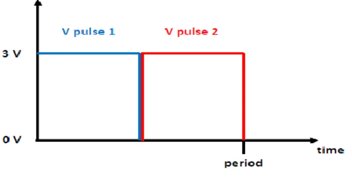
- 34 - additional external ports are used to bias the switches. Note that an asymmetric time-periodic sequence is used which means that the two biases must be two rectangular pulses with duty-cycle = 50%: one ON-OFF, the other OFF-ON. This is requested by the first step of the WPT procedure described in Chapter 2, in order to have localization capabilities.
Figure 2.2.2 First Bias On and Second Bias OFF
We use a traditional microwave Schottky diode as switching element and we refer to typical parameters values taken for its model description. In the examples we will use a “reference diode” with a sufficiently high cutoff frequency, whose model parameters are: saturation current Is=5 nA, junction capacitance Cj0 = 1fF, slope factor of conduction current α =
38.696V−1 , built-in (diffusion) potential φ=0.7 V, series resistance
.Rs = 6Ω.
Now we perform the nonlinear system analysis procedure, we perform an analysis by means of
an envelope HB simulation with a 2.45 GHz carrier and the periodic time-based waveforms for the two switches, as described in Figure 2.2.2 in order to calculate the far-field radiation patterns in the xz (or φ=0𝑜 ) plane. The analysis under-modulated regime is performed by considering a switch modulation frequency 𝑓𝑀 ≪ 𝑓0 equal to 1 MHz. Use Rectangular pulses sources with
repetition period 𝑇𝑀 =1 us and amplitude 𝑉𝑏𝑖𝑎𝑠 =3 V are applied at the two bias ports. Below
voltage sources that we use our circuit in time domain as we perform our simulation according to Envelope HB principles.
- 35 -
Here is what we get (when running an envelope simulation to ON-OFF/OFF-ON state) in ADS at two sources for biasing
Where 5001 is totally arbitrary. The envelope simulation basically is a time varying harmonic balance, this is why v1 is a freq domain signal (or a set of freq domain signals).
- 36 -
ts(v1) will provide the Fourier transform of v1. ts(v1,0,5e-6,5001) is the numerical Fourier transform of v1, between 0 and 5 us, with 5001 time steps, but this is not necessarily related to the time step that we choose in the envelope setup. It is the number of points that we will get to describe the transformed signal.
In other words, we don’t need to simulate 5001 time points. Of course if our time step is too coarse we will not catch the proper t_rise and t_fall.
Note that if we plot ts(v1), then t_start, t_stop and number of points will be at the default value that can lead to a not accurate Fourier transform.
After performing the envelope EM-cosimulation in ADS we get the results in electrical
quantities, as in the figures below, where we can see the antenna input currents envelopes and the corresponding zoom on the right (the short period of the carrier inside the long modulation one is clearly visible).
When we try to see the far-field at fundamental frequency @2.45 GHz, it shows that Envelope engine is not supported to see the far-field. We can run EM Circuit Excitation either with transient or with harmonic balance. In this case, we need to modify the sources accordingly (they will be all time domain or all freq domain sources, depending on the type of analysis). Primarily our goal was to make the envelope co-simulation with the antenna element and trying to obtain the far-field at the fundamental
- 37 - (2.45 GHz) and at the harmonics (2.45 GHz +- modulation frequency). Due to this fact we stop our envelope co simulation and move to standard harmonic balance simulation which is much heavier but still supported by ADS software.
2.3 ADS Harmonic Balance Inter-modulation Analysis
Previously, we encountered a problem in Envelope Co-simulation that we were unable to perform EM-circuit excitation to see far-field at fundamental frequency. Now in this section we perform and analyze the standard HB inter-modulation simulation with the same 2-array element monopole to see the normalized far-field at different resonant frequencies.
Non-Linear and Full Wave Co-Simulation
This method includes EM/nonlinear analysis of the entire radiating structure by combining the standard (not envelope-based) harmonic balance approach for the precise illustration of the non-linearities, the broadband full wave of the array and its feeding network. An array in this case with 𝑛𝐴 ports (identical in terms of switches numbers), description of the EM-based structure will consists of 𝑛𝐴 +1-port network (input RF port included).
Detailed theory of Wireless Power Transfer Approach in Two Step
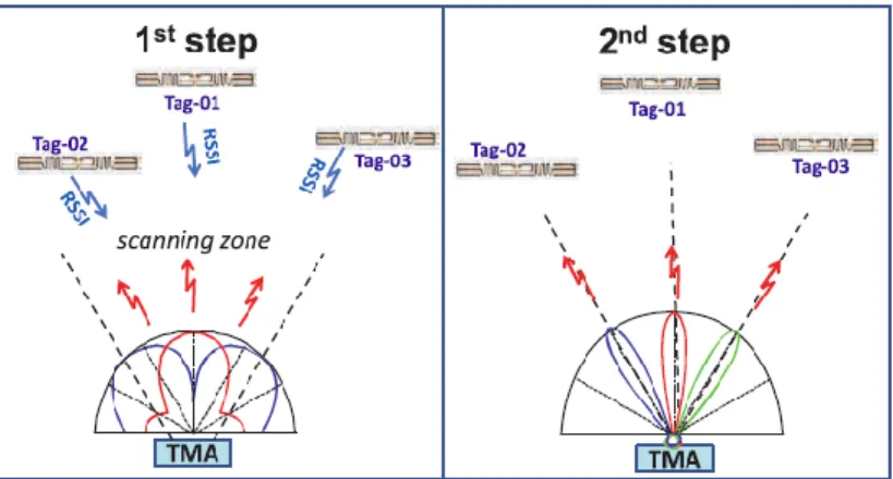
The WPT two-step procedure exploiting TMAs considers several sensors are equipped with rectennas and are placed randomly inside room as per idea. A linear TMA is fully deployed with dynamic reconfigurability in a novel WPT 2-step procedure, as represented in Fig 2.3.1 [1]: in the first step only two elements of the TMA are periodically driven to localize 𝑁𝑡𝑎𝑔𝑠. While in
the second step, the entire 𝑛𝐴-element array is used to precisely energize the previously detected tags. We take advantage, in both phases from the capability of TMA to perform a multiple radiation at the fundamental and the first sideband harmonics 𝑓0+𝑓𝑀. In practice in my work, I have tried to reproduce the first step of this procedure with ADS.
- 38 -
Figure 2.3.1 WPT procedure in 2-steps exploiting a linear TMA. Step-1: Localization of tags, Step-2: power transmission to the
previously detected tags.
In the first case we modify our circuit with one RF power generator of -0dbm and also change the voltage sources to Vn_tones in frequency domain as we perform a simulation in the frequency domain. Of course, we need to select a sufficiently high number of harmonics (ℎ) to accurately describe through Foureir transformation the bias pulses in the frequency domain. ℎ=50 was selected as a good tradeoff between accuracy and complexity of the simulation
Then we have included two "Vn_tones" sources where we have to enter the 51 values of frequencies (including DC) and the 51 complex amplitudes (V[1], V[2],...) through the "polar" command.
- 39 -
The sideband input HB generators at h*F2 (with h=0,1,2,...,50) have the values obtained from the Fourier transformation of the two bias waveforms. Corresponding to the following indexes:
indexes 0 0 --> 0 Hz indexes 0 1 --> 100 kHz indexes 0 2 --> 200 kHz ...
indexes 0 100 --> 10 MHz
For the First bias we have to input the values given below;
Frequency (Hz) Amplitude of the corresponding generator
Phase of the corresponding generator
1. 0.000000E+00 0.150000E+01 0.000 2. 0.100000E+06 0.190986E+01 -90.180 3. 0.200000E+06 0.000000E+00 0.000 4. 0.300000E+06 0.636629E+00 -90.540 5. 0.400000E+06 0.000000E+00 0.000 6. 0.500000E+06 0.381988E+00 -90.900 7. 0.600000E+06 0.000000E+00 0.000 8. 0.700000E+06 0.272859E+00 -91.260 9. 0.800000E+06 0.000000E+00 0.000 10. 0.900000E+06 0.212235E+00 -91.620 11. 0.100000E+07 0.000000E+00 0.000 12. 0.110000E+07 0.173658E+00 -91.980 13. 0.120000E+07 0.000000E+00 0.000 14. 0.130000E+07 0.146953E+00 -92.340 15. 0.140000E+07 0.000000E+00 0.000 16. 0.150000E+07 0.127371E+00 -92.700 17. 0.160000E+07 0.000000E+00 0.000 18. 0.170000E+07 0.112398E+00 -93.060 19. 0.180000E+07 0.000000E+00 0.000 20. 0.190000E+07 0.100579E+00 -93.420 21. 0.200000E+07 0.000000E+00 0.000 22. 0.210000E+07 0.910117E-01 -93.780 23. 0.220000E+07 0.000000E+00 0.000 24. 0.230000E+07 0.831097E-01 -94.140 25. 0.240000E+07 0.000000E+00 0.000 26. 0.250000E+07 0.764730E-01 -94.500 27. 0.260000E+07 0.000000E+00 0.000 28. 0.270000E+07 0.708204E-01 -94.860 29. 0.280000E+07 0.000000E+00 0.000
- 40 - 30. 0.290000E+07 0.659484E-01 -95.220 31. 0.300000E+07 0.000000E+00 0.000 32. 0.310000E+07 0.617059E-01 -95.580 33. 0.320000E+07 0.000000E+00 0.000 34. 0.330000E+07 0.579783E-01 -95.940 35. 0.340000E+07 0.000000E+00 0.000 36. 0.350000E+07 0.546775E-01 -96.300 37. 0.360000E+07 0.000000E+00 0.000 38. 0.370000E+07 0.517342E-01 -96.660 39. 0.380000E+07 0.000000E+00 0.000 40. 0.390000E+07 0.490935E-01 -97.020 41. 0.400000E+07 0.666458E-16 151.200 42. 0.410000E+07 0.467110E-01 -97.380 43. 0.420000E+07 0.000000E+00 0.000 44. 0.430000E+07 0.445507E-01 -97.740 45. 0.440000E+07 0.000000E+00 0.000 46. 0.450000E+07 0.425830E-01 -98.100 47. 0.460000E+07 0.000000E+00 0.000 48. 0.470000E+07 0.407833E-01 -98.460 49. 0.480000E+07 0.000000E+00 0.000 50. 0.490000E+07 0.391311E-01 -98.820
And For the Second bias we have to input below Values
Frequency (Hz)
Amplitude of the corresponding generator
Phase of the corresponding generator 1. 0.000000E+00 0.150000E+01 0.000 2. 0.100000E+06 0.190986E+01 90.180 3. 0.200000E+06 0.000000E+00 0.000 4. 0.300000E+06 0.636629E+00 90.540 5. 0.400000E+06 0.000000E+00 0.000 6. 0.500000E+06 0.381988E+00 90.900 7. 0.600000E+06 0.000000E+00 0.000 8. 0.700000E+06 0.272859E+00 91.260 9. 0.800000E+06 0.000000E+00 0.000 10. 0.900000E+06 0.212235E+00 91.620 11. 0.100000E+07 0.000000E+00 0.000 12. 0.110000E+07 0.173658E+00 91.980 13. 0.120000E+07 0.000000E+00 0.000 14. 0.130000E+07 0.146953E+00 92.340
- 41 - 15. 0.140000E+07 0.000000E+00 0.000 16. 0.150000E+07 0.127371E+00 92.700 17. 0.160000E+07 0.000000E+00 0.000 18. 0.170000E+07 0.112398E+00 93.060 19. 0.180000E+07 0.000000E+00 0.000 20. 0.190000E+07 0.100579E+00 93.420 21. 0.200000E+07 0.000000E+00 0.000 22. 0.210000E+07 0.910117E-01 93.780 23. 0.220000E+07 0.000000E+00 0.000 24. 0.230000E+07 0.831097E-01 94.140 25. 0.240000E+07 0.000000E+00 0.000 26. 0.250000E+07 0.764730E-01 94.500 27. 0.260000E+07 0.000000E+00 0.000 28. 0.270000E+07 0.708204E-01 94.860 29. 0.280000E+07 0.000000E+00 0.000 30. 0.290000E+07 0.659484E-01 95.220 31. 0.300000E+07 0.000000E+00 0.000 32. 0.310000E+07 0.617059E-01 95.580 33. 0.320000E+07 0.000000E+00 0.000 34. 0.330000E+07 0.579783E-01 95.940 35. 0.340000E+07 0.000000E+00 0.000 36. 0.350000E+07 0.546775E-01 96.300 37. 0.360000E+07 0.000000E+00 0.000 38. 0.370000E+07 0.517342E-01 96.660 39. 0.380000E+07 0.000000E+00 0.000 40. 0.390000E+07 0.490935E-01 97.020 41. 0.400000E+07 0.666458E-16 151.200 42. 0.410000E+07 0.467110E-01 97.380 43. 0.420000E+07 0.000000E+00 0.000 44. 0.430000E+07 0.445507E-01 97.740 45. 0.440000E+07 0.000000E+00 0.000 46. 0.450000E+07 0.425830E-01 98.100 47. 0.460000E+07 0.000000E+00 0.000 48. 0.470000E+07 0.407833E-01 98.460 49. 0.480000E+07 0.000000E+00 0.000 50. 0.490000E+07 0.391311E-01 98.820
Then it is sufficient to have just two harmonics for 2.45 GHz (Order = 2) (otherwise the simulation is too heavy), whereas we need an Order = 50 for the modulation frequency. As
- 42 -
regards the Max-order, at least 51 should be placed, in order to have all the lines around the fundamental (2.45 GHz +- n*f_mod).
We define both fundamental frequencies in the HB controller with the number of harmonics and we need to have consistent settings between sources and HB controller, that is the same number of harmonics used to build the pulse have to be used in the HB controller. We can start our simulation using 50 harmonics. Therefore we have to create a simulation with F1 = 2.45 GHz, and F2=100 kHz.The fundamental input HB generator at F1 will be the usual one (freq. corresponding to indexes 1 0)
Later we can see the far-field results will be extracted at the frequencies: 1 0 (=2.45 GHz) for the SUM pattern
1 1 (=2.4501 GHz) for the DIFFERENCE pattern
1 -1 (=2.4499 GHz) for the DIFFERENCE pattern (identical to the previous one)
We have to notice that the frequency of the (excitation) source in HB simulation tool must be included in the solution frequencies of the antenna analysis in momentum. Thus, if we want to see the results of F=2.45 GHz, 2.4501 GHz and 2.4499GHz, we should have exactly the far-field and near-filed results of the antenna in this frequency. In our case in frequency definition in momentum should be adjust like this in below image:
- 43 -
- 44 -
Localization Step-1
By driving these switches properly, an interesting direction finding functionality of two-element TMA is deployable exploiting the TMA sideband radiation SBR. We choose a complementary control sequence of the kind reported in Figure. 2.3.2 With solid lines (i.e., 50% of duty cycle for both switches) [1] to obtain from the two-element array symmetric radiation surfaces both of the sum type Σ at 𝑓0(two elements in-phase), and of the difference type Δ, but at 𝑓0+𝑓𝑀 (two elements out-of-phase). Figure 2.3.2. also shows the tuning parameter allowing a variable overlapping percentage of the control sequences [1]: in this way beam steering of the Δ pattern is achieved in the scanning plane (-90𝑜 < 𝜃 < 90) increasing 𝑑 results in a shift increase of the Δ null in the right half-plane at (−0𝑜 < 𝜃 < 90) a symmetric result in the left half-plane (-90𝑜 < 𝜃 < 0) is observed at 𝑓0+𝑓𝑀.
Figure.2.3.2 Switches driving sequences of a two-element array for localization purposes 𝑑 is the pulse shape design parameter
for pattern steering.
The steering Δ pattern is made possible by the complex nature of the corresponding Fourier coefficient 𝑢+𝑙𝑖in eqn (2). Conversely, the real coefficient 𝑢0𝑖 is responsible for the fixed nature
of the Σ pattern, while changing 𝑑.
That sensor identifications (IDs) have been already acquired by standard RF identification (RFID) reading operations of passive tags. The (flat) Σ pattern of a standard (unmodulated)
two-element array could be used for this purpose. When tag IDs are acquired, the true scanning phase takes place, by exploiting the time modulation according to the patterns of Figure. 2.3.2. The sharp nulls of the steered Δ patterns allow high resolution in the tags detection: the
backscattered received signal strength indicators (RSSIs) due to the Δ and Σ patterns can be suitably combined to build the maximum power ratio (MPR),
The combination of the radar monopulse operating principle with the scanning capability has proven its effectiveness in indoor localization, with resolution up to a few cm at 2.45 GHz. At
- 45 -
the end of the scanning activity a vector with the 𝑁𝑡𝑎𝑔 values of corresponding to the peaks of
the received MPRs (θ𝑝𝑒𝑎𝑘) is recorded.
Power Transfer Step-2
Once the tags positions have been detected, the entire array is driven by a proper control sequence involving all the switches and providing the desired radiation properties. From this side, there is plenty of optimization strategies for the engineering of the radiation patterns shape of ideal TMAs. In particular, it is possible to add, as an additional design parameter, the maximum radiation direction at the sideband harmonics 𝑓0+ℎ𝑓𝑀 (ℎ ≠ 0). In this way it is possible to point the sideband harmonic radiation in the desired direction, and this can be done
simultaneously at several near-carrier frequencies(ℎ ≥ 1).
Now, perform the EM-circuit excitation for HB simulation to extract the far field radiation pattern at multiple resonant frequencies.
Left image refers to the extracted far-field at f=2.4490 GHz
- 46 - Above image refers to the extracted far-field at f=2.4500 GHz
Right image refers to the extracted far-field at f=2.4501 GHz
- 47 -
While the corresponding far-field radiation patterns (in the xz plane) are given below, and they correspond to the theoretical ones:
1. At f=2.4499Ghz (φ, 𝜃)
Figure 2.3.3.(A) Δ pattern @ 𝑓0+𝑓𝑀
- 48 - 2. At f= 2.4500Ghz (φ, 𝜃)
Figure 2.3.3 (A) Σ pattern @𝑓0
- 49 - 3. At f= 2.4501 Ghz (φ, 𝜃)
Figure 2.3.3.(A) Δ pattern @ 𝑓0+𝑓𝑀
- 50 -
In order to check the tuning capability of the Difference pattern by acting on the duty-cycle (d) of the biases, now we consider for 𝒅 = 8%, For the First bias we have to input below values
Frequency (Hz) Amplitude of the corresponding generator Phase of the corresponding generator
1. 0.000000E+00 0.174000E+01 0.000 2. 0.100000E+06 0.184986E+01 -104.580 3. 0.200000E+06 0.460044E+00 -29.160 4. 0.300000E+06 0.464083E+00 -133.740 5. 0.400000E+06 0.403147E+00 -58.320 6. 0.500000E+06 0.118041E+00 -162.900 7. 0.600000E+06 0.317701E+00 -87.480 8. 0.700000E+06 0.511287E-01 -12.060 9. 0.800000E+06 0.216034E+00 -116.640 10. 0.900000E+06 0.135284E+00 -41.220 11. 0.100000E+07 0.112277E+00 -145.800 12. 0.110000E+07 0.161463E+00 -70.380 13. 0.120000E+07 0.199521E-01 -174.960 14. 0.130000E+07 0.145794E+00 -99.540 15. 0.140000E+07 0.502352E-01 -24.120 16. 0.150000E+07 0.103045E+00 -128.700 17. 0.160000E+07 0.920120E-01 -53.280 18. 0.170000E+07 0.478568E-01 -157.860 19. 0.180000E+07 0.104279E+00 -82.440 20. 0.190000E+07 0.631538E-02 -7.020 21. 0.200000E+07 0.908790E-01 -111.600 22. 0.210000E+07 0.487665E-01 -36.180 23. 0.220000E+07 0.594741E-01 -140.760 24. 0.230000E+07 0.728296E-01 -65.340 25. 0.240000E+07 0.198089E-01 -169.920 26. 0.250000E+07 0.764730E-01 -94.500 27. 0.260000E+07 0.182881E-01 -19.080 28. 0.270000E+07 0.620604E-01 -123.660 29. 0.280000E+07 0.467527E-01 -48.240 30. 0.290000E+07 0.353369E-01 -152.820 31. 0.300000E+07 0.606359E-01 -77.400 32. 0.310000E+07 0.387454E-02 178.020 33. 0.320000E+07 0.587248E-01 -106.560 34. 0.330000E+07 0.246860E-01 -31.140 35. 0.340000E+07 0.433639E-01 -135.720 36. 0.350000E+07 0.442350E-01 -60.300
![Figure 2.1 shows a window for determining the substrate structure[4]. On the menu bar of the ADS Layout window, select Momentum > Substrate > Create/Modify to display the window shown in Figure 2.2](https://thumb-eu.123doks.com/thumbv2/123dokorg/7427290.99353/24.918.266.656.677.903/figure-determining-substrate-structure-momentum-substrate-display-figure.webp)
![Figure 2.3 is a conductor shape drawn on the layer named cond[4]. A microstrip line having a 25-mil width and 100-mil length is inserted on the substrate shown in Figure 2.1 and 2.2](https://thumb-eu.123doks.com/thumbv2/123dokorg/7427290.99353/25.918.270.653.767.1036/figure-conductor-microstrip-having-length-inserted-substrate-figure.webp)
![Figure 2.6. Shows the window after completing the port setup[4]. The reference lines can be moved by entering the Reference Offset parameter in the Port Properties Editor window and can also be moved using the mouse by selecting the reference line and dr](https://thumb-eu.123doks.com/thumbv2/123dokorg/7427290.99353/26.918.279.643.233.492/completing-reference-entering-reference-parameter-properties-selecting-reference.webp)