Simulation of Silicon Hetero-junction
Solar Cells
Urs Aeberhard1,∗, Philippe Czaja1, Markus Ermes1, Bart E. Pieters1, Ganna Chistiakova1, Karsten Bittkau1, Alexei Richter1, Kaining Ding1, Simone Giusepponi2 and Massimo Celino2
1IEK-5 Photovoltaik, Forschungszentrum J¨ulich, D-52425 J¨ulich, Germany 2ENEA, C.R. Casaccia, Via Anguillarese 301, 00123 Rome, Italy
*Corresponding Author: [email protected]
Received 5 November 2015; Accepted 3 June 2016; Publication 1 August 2016
Abstract
The silicon hetero-junction (SHJ) technology holds the current efficiency record of 25.6% for silicon-based single junction solar cells and shows great potential to become a future industrial standard for high-efficiency crystalline silicon (c-Si) cells. One of the main advantages of this concept over other wafer based silicon technologies are the very high open-circuit voltages that can be achieved thanks to the passivation of contacts by thin films of hydrogenated amorphous silicon (a-Si:H). The a-Si:H/c-Si interface, while central to the technology, is still not fully understood in terms of transport and recombination across this nanoscale region, especially concerning the role of the different localized tail and defect states in the a-Si:H and at the a-Si:H/c-Si interface and of the band offsets and band bending induced by the heterostructure potential and the large doping, respectively. For instance, a consistent microscopic picture of transport and recombination processes with treatment of thermal and tunneling mechanisms on equal footing is lacking. On the other hand, there are new SHJ device architectures like thin wafers with light trapping structures [1] or interdigitated back contact (IBC) cells [2], which define additional requirements for the modelling approach concerning the integration of 3D Journal of Green Engineering, Vol. 5, 11–32.
doi: 10.13052/jge1904-4720.5342 c
optical and electrical simulations. This paper provides an overview over our current efforts in the creation of a multi-scale and multi-physics framework to deal with the challenges encountered in the simulation of SHJ solar cells.
Keywords: Multiscale simulation, silicon heterojunction, solar cell.
1 Introduction
A silicon heterojunction (SHJ) solar cell is defined by a high quality crystalline silicon wafer being combined with another semiconductor material, usually a thin film. The crystalline Si (c-Si) enables carrier absorption and transport, while the thin films form the carrier selective contacts and passivate the highly recombination-active interface. Consequently, using non – c-Si films for charge carrier extraction introduces a distinctive interface area between the two materials characterized by offsets in the conduction and the valence bands, defect states and the distribution of charges. All of these determine the electrical transport across the heterojunction and the recombination of generated charge carriers. This recombination of charge carriers then strongly affects the open circuit voltage (Voc) of the solar cell. Currently, highly P-and B-doped films of hydrogenated amorphous silicon (a-Si:H) are used as the emitter or to induce band bending and thereby provide a front- or back surface field to ensure an efficient charge carrier extraction. All the while, the passivation is predominantly provided by intrinsic a-Si:H films. These enable Voc values up to 750 mV [3] accompanied by a low temperature coefficient. Generally, the passivation mechanism of a-Si:H layers is attributed to hydrogen (H) passivating dangling bonds at the c-Si surface. Nevertheless, the detailed impact of these defect states and the band structure at the hetero-interface on the transport and the recombination mechanisms are still poorly understood. Especially, nowadays more sophisticated device structures like bifacial SHJ solar cells or high performance IBC solar cells [4] necessitate an optical and electrical 3D modeling of these devices in a multi-scale approach. Additionally, new device concepts with novel, particularly dopant-free, thin films for charge carrier extraction [4, 5] would strongly benefit from a deeper understanding of the processes defining the properties of the heterojunction.
In general, the opto-electronic simulation of solar cell devices can be divided in an optical part, where the propagation and attenuation of the light inside the solar cell is computed, and an electronic part covering the photogeneration and transport of charge carriers for extraction at the contacts as well as the injection and recombination of charge carriers at finite splitting
of contact Fermi levels. Under standard conditions, the intensity of the electromagnetic field is used to determine the local photogeneration rate via the local absorption rate, implicitly assuming unit generation efficiency. If photon recycling can be neglected, which is usually the case for non-radiatively limited solar cells under one sun illumination, no feedback to the optical model is required, and the two problems can thus be solved sequentially by independent approaches. On the other hand, in a comprehensive modelling approach suitable for the description of the devices in Figure 1, both electronic and optical simulations represent individual multiscale modelling challenges. This difficulty originates from the simultaneous presence of electronically or optically thin components, such as the passivation layers or anti-reflection coatings, which require a rigorous treatment of either the electronic structure (quantum mechanics) or the optical properties (wave optics) with very high spatial resolution, and of extended bulk components, such as the micron-sized wafer and the front side texture, which have to be treated by effective macroscopic semiconductor equations and ray optical approaches. The main challenge thus resides in combining these methods into a comprehensive approach that allows one to project the effects of the local micro- or nanos-tructure onto the global device characteristics. The aim of this paper is to provide an overview of our current work on the different steps towards such a multi-scale and multi-physics simulation framework for SHJ solar cells.
The paper is organized as follows. In Section 2, the electronic models are described on micro-, meso- and macroscopic scales. Section 3 covers the optical simulation of both flat and textured SHJ devices. A brief summary and the main conclusions are presented in Section 4.
Figure 1 Silicon heterojunction architectures investigated at IEK-5 Photovoltaik in J¨ulich: (a) thin SHJ devices with ray optical and nanophotonic light trapping, representing a 3D optical multiscale problem; (b) SHJ with interdigitated back contact (IBC), requiring 3D electronic simulations.
2 Electronic Simulation
The presence of the amorphous phase with the inherent disorder and of the amorphous-crystalline interface with its own set of interfacial defect states necessitate an atomistic description at the nanoscale of the amorphous material and the interface region for a valid picture of the electronic (and vibrational) states participating in the dominant transport and recombination processes. The dynamics of the charge carriers at the interface is best captured in a mesoscopic quantum transport model including both thermionic emission and defect assisted tunneling under consideration of the actual phonon modes. The mobilities and recombination rates resulting from the mesoscopic approach can then be used to project the impact of specific interfacial configurations from the local charge carrier dynamics to the global device characteristics, using the standard macroscopic semiconductor transport equations with inter-band generation and recombination rates. In the case of textured interfaces used for light trapping purposes, or in the presence of complex contact geometries such as those required by the IBC concept in Figure 1(b), the equations may need to be solved in more than one spatial dimension. While at the early stage of development presented here the problems at different scales are treated independently, a major focus of future work will lie on the interfacing of the individual micro-, meso-, and macroscopic models, integrating them in a comprehensive multiscale approach as shown in Figure 2.
2.1 Microscopic Electronic Structure
The atomic and electronic structure at the amorphous-crystalline interface is the starting point of any investigation targeting the impact of the interface properties on the device characteristics. The microscopic picture of the com-plex interfacial region is best captured by ab initio descriptions of the material [7, 8], allowing for a comprehensive assessment of the device-relevant states, from localized mid-gap defects to extended bands for mobile carriers.
2.1.1 Atomic Structure
The ab initio PWscf (Plane-Wave Self-Consistent Field) code of theQuantum ESPRESSO suite is used [9, 10] to perform Born-Oppenheimer Molecular Dynamics (BOMD) simulations of the a-Si:H/c-Si interface. PWscf performs many different kinds of self-consistent calculations of electronic structure properties within Density-Functional Theory (DFT) [11, 12], using a Plane-Wave (PW) basis set and pseudopotentials (PP). We use the Si and H ultrasoft pseudopotentials with Perdew-Burke-Ernzerhof (PBE) [14] approximant
Figure 2 Multiscale scheme for the electronic simulation of SHJ devices to propagate local material properties at the interface via meso-scale charge carrier dynamics in the heterojunction region to performance-relevant features in the global device characteristics.
GGA exchange-correlation potential, available in the Quantum ESPRESSO library [10].
In view of the large-scale molecular dynamics simulations, a supercell approach is used to simulate the a-Si:H/c-Si interface with periodic boundary conditions (PBC) meant to mimic an infinitely extended system. The structure is infinitely extended in both x and y directions. To suppress the interaction between the external surfaces due to PBC, a void region of about 10 Å is considered. This distance was checked by a convergence test with respect to the size of the void.
As shown in Figure 3(a), the interface is built by bringing into close proximity two free surfaces obtained from cutting both the crystalline silicon and the hydrogenated amorphous silicon. The relaxed p(2 × 1) symmetric reconstruction of the Si(001) surface constitutes the c-Si side of the interface. It is formed by 192 Si atoms: 12 layers of silicon each of them with 16 atoms. The a-Si:H side of the system is generated using a quench from the melt simulation protocol, currently used to generate high-quality amorphous samples [7]. It is composed of 128 Si atoms and 16 H atoms to have a concentration percentage of about 11% that is the nominal concentration targeted in experimental materials optimized for PV performance [13]. The total length of the system is
Figure 3 (a) Snapshot of the initial a-Si:H/c-Si interface in the simulation box. The structure is infinitely extended in both x and y directions. A void region is considered to suppress the interaction, due to periodic boundary conditions, between the external surfaces. Free surfaces and a-Si:H/c-Si interface are perpendicular to the y axis. Hydrogen atoms are in blue, silicon atoms are in dark yellow in the c-Si side and are in light yellow in the a-Si:H side. (b) Snapshot of the a-Si:H/c-Si interface in the simulation box at 35 ps of MD simulation.
Lz= 38.70 Å, while in the x and y direction the system has Lx= Ly= 15.48 Å. Total energy calculations of the interface at different distances between c-Si and a-Si:H were performed to find the interface configuration corresponding to the lowest total energy. The configurations were built by moving rigidly by hand the a-Si:H part and keeping fixed the c-Si one.
The interface shown in Figure 3(a) is used as starting configuration for a MD simulation on the electronic ground state at constant volume and constant temperature (NVT). The ionic temperature is fixed at T = 300 K and is controlled using an Andersen thermostat. The first four layers of c-Si atoms on the left are kept fixed to impose a bulk-like behaviour on the crystalline silicon part of the system. The MD simulation is performed for more than 35 ps, the initial part of the simulation (20 ps) was used to thermalize the system and reach a stable configuration. Figure 3(b) displays a snapshot of the a-Si:H/c-Si interface at 35 ps in which thermal displacements are also shown.
2.1.2 Electronic Structure
We use density functional theory (DFT) [11, 12] to self-consistently calculate the electronic structure of the interface configurations. The calculations are done with the PWPP code Quantum ESPRESSO [9, 10] using ultrasoft pseudopotentials with the PBE-GGA exchange-correlation functional [14].
Subsequent to the electronic structure calculation the wave functions (ψ) and electronic density of states (DOS) are analyzed to obtain information about the local microscopic properties of the interface, which are relevant for the mesoscopic dynamics and macroscopic device characteristics. In particular, the wave function localization is analyzed qualitatively and quantitatively to allow for the distinction of localized states and the identification of their origins. In combination with the local DOS the contribution of dangling bonds and interfaces to the important mid-gap states can be determined.
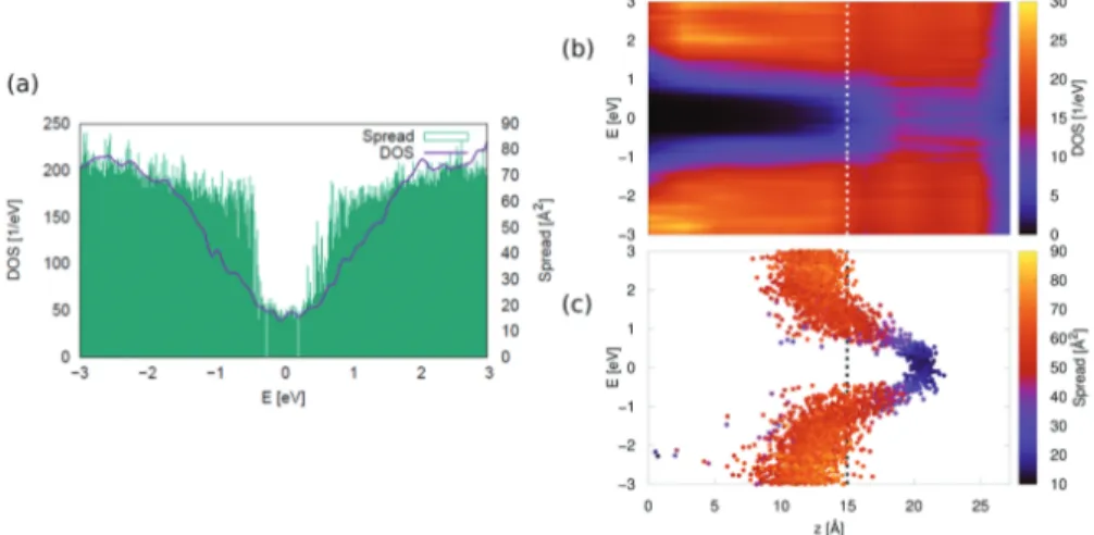
As a quantitative measure for the wave function localization we use the spreadS, which is calculated as the variance of |ψ|2with respect to one unit cell. Analogously the center of the wave function is given by the center of mass of|ψ|2. In Figure 4(a) the spread in z-direction (i.e., in growth direction)
Szis shown as a function of the wave function energy together with the total density of states around the Fermi energy for the above described interface
Figure 4 (a) DOS and wave function spread (in direction perpendicular to the interface) in the energy region around the Fermi energy. (b) Local DOS integrated over layers parallel to the interface as a function of the z-coordinate. (c) Wave function spread in z-direction. Each dot marks the energy and the position of the center of one wave function, where the color represents its spread. The dotted line shows the approximate position of the interface.
configuration. The figure shows that there is a dense distribution of strongly localized states inside the c-Si band gap, which can be clearly distinguished from the more extended tail and bulk states. The origin of these states can be investigated further by looking at the local DOS and the wave function centers as shown in Figures 4(b) and (c), respectively. In (b), the layer-resolved DOS is displayed as a function of the z-coordinate, which is obtained by integrating the local DOS over layers parallel to the interface. In (c),Sz is plotted as a function of the energy and the z-component of the center of the wave functions. Each dot marks the energy and the position of one wave function, i.e., where along thez-direction it is centered. The color of each dot represents the spread of the wave function. These results indicate that the contribution to the mid-gap states comes mainly from localized states in the a-Si:H layer, whereas the interface region hardly contributes at all. More information about these localized states can still be obtained by looking at the localization in all three dimensions and relating the wave function centers to the atomic structure.
2.2 Mesoscopic Carrier Dynamics
Transport and recombination across the c-Si/a-Si:H interface has been inves-tigated so far mostly in the framework of the semiclassical approximation, where simplified models for the local electronic structure are combined with conventional macroscopic semiconductor transport equations [6]. In our simulation effort presented here, we complement this approach by quantum transport calculations that are able to capture non-classical phenomena such as direct and phonon-assisted tunneling, which are likely to play an important role in the transport and recombination processes at the interface.
The simulations are performed using the in-house code PVnegf that is based on an implementation of the non-equilibrium Green’s function formalism (NEGF) customized for photovoltaic device applications [15]. In a first approach, a simple effective mass model is used to describe the electronic structure of valence and conduction bands [16]. The implementation includes coupling to photons as well as to acoustic and non-polar optical phonons, which provide intraband relaxation as well as indirect optical transitions [17].
Here, we show the application of the formalism to the simulation of hole currents over abrupt a-Si:H/c-Si interfaces at the p-contact of a-Si:H/c-Si solar cells grown on p-type wafers. At this stage, defects are neglected in the transport across the interface, i.e., transport is restricted to direct and
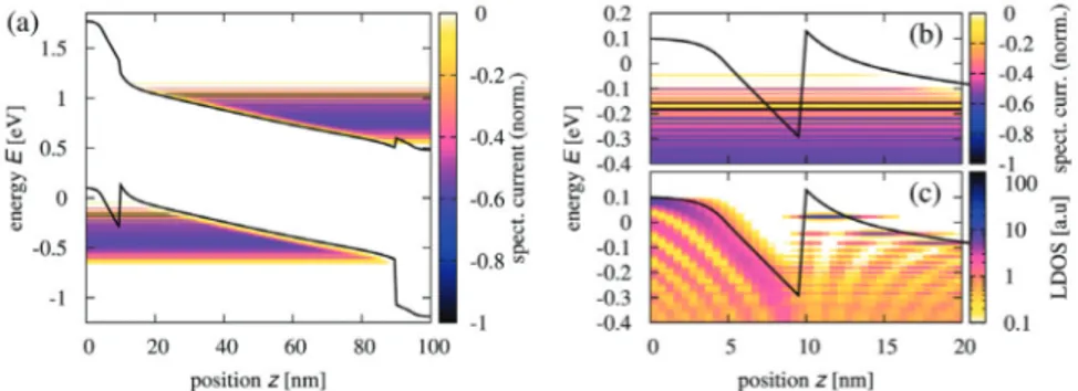
phonon assisted tunneling as well as thermionic emission over the interfacial barrier. Also, the ITO layer is not included in the simulation beyond providing a Schottky contact boundary condition. Figure 5(a) displays the energy resolved photocurrent flow in an ultra-thinp-i-n SHJ architecture under monochromatic illumination withEphot = 1.2 eV and Iphot = 0.1 kW/m2 and forward bias
Vbias = 0.5 V. The a-Si:H component is composed of a p/i layer stack, similar to the configuration described in [23]. While realistic SHJ exhibit an essentially field-free absorber region, the situation at the p-interface in terms of band bending and offsets is very similar to the one described here. As can be verified in Figures 5(b) and (c), there is a strong impact of built-in fields and of the discretization of the local density of states on the current spectrum in the interface region.
For a more realistic mesoscopic picture of charge carrier transport and recombination across the a-Si:H/c-Si interface, the present approach needs to be extended in several directions. In terms of the transport channels, defect-assisted tunneling needs to be added. On a phenomenological level, this can be achieved via coupling to an independent set of defect states, similar to the phenomenological treatment of defect assisted recombination [18]. For a consistent treatment of transport via localized and extended states, one needs to resort to an atomistic description of the electronic structure [19]. Finally, the mesoscopic approach needs to be embedded in a macroscopic description of the extended device via coupling to the drift-diffusion transport picture in a concurrent multiscale framework [20].
Figure 5 (a) Spectral photocurrent flow in an ultra-thinp-i-n SHJ device under monochro-matic illumination (Ephot = 1.2 eV, Iphot = 0.1 kW/m2) at a forward bias voltage of
Vbias= 0.5 V, exhibiting current contributions from tunneling and emission over the barrier. (b) Photocurrent flow across the interface region, revealing the strong impact of (c) the local DOS (1D) with discretization from the doping-induced potential well.
2.3 Macroscopic Device Characteristics
The macroscopic level is where most simulation studies of SHJ devices have been performed so far. WithAF ORS − HET [21], there is even a dedicated device simulation tool for this device type. However, its restrictions to 1D geometries limit its applicability to the structures with 3D features under investigation here. Among similar device simulators,ASA [22] provides a more advanced description of defect-related properties, but has similar limi-tations in terms of dimensionality and tunneling models. The most advanced 1D device simulation performed so far for the SHJ structure was based on the commercial 3D TCAD tool Sentaurus from Synopsys, which features a Wentzel-Kramers-Brillouin tunneling model that is able to capture some of the qualitative effects of tunneling on the device characteristics [23].
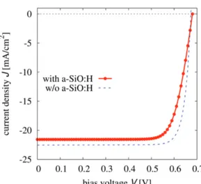
Here, we show basic 1D simulations of a silicon oxide based SHJ [24] using the Sentaurus TCAD tool. At this stage, tunneling is not included in the description. The material data is taken from the literature (electronic properties) or measured-inhouse (optical data). The simulated band profile corresponding to the layer stack of an all-oxide SHJ with flat interfaces as shown in Figure 6(a) at short circuit conditions and under AM1.5 illumination is displayed in Figure 6(b). The current-voltage characteristics under AM1.5 illumination are given in Figure 7. For comparison, the JV-curve of the same structure, but without the thin a-SiOx:H layers is shown as well. In the
Figure 6 (a) Schematic layer stack of an all-oxide SHJ device architecture as experimentally investigated at IEK-5. (b) Corresponding band profile and quasi-Fermi levelsEF n,p (for majorities) as computed with the Synopsys Sentaurus TCAD tool (the ITO-Ag is treated as an ohmic contact) at short circuit conditions and under AM1.5 illumination.
Figure 7 Current-voltage characteristics of the all-oxide SHJ device with (solid line with symbols) and without (dashed line) a-SiOx:H passivation layers. At the absence of tunneling contributions to carrier extraction, the introduction of the a-SiOx:H barriers leads to a decrease of both short-circuit current and fill-factor at slightly increased open-circuit voltage.
simulation, the presence of the a-SiOx:H layers leads to a reduction of both short circuit current and fill factor at slightly increased open circuit voltage. This points at an insufficient carrier extraction efficiency, which is expected to be partially mitigated by the introduction of efficient tunneling processes. Experimentally, the absence of passivation layers results in a strong reduction ofVoc to values below 600 mV. Hence, the models for loss processes and passivation are not yet satisfactory at this stage of the implementation.
Two-dimensional electrical simulations of SHJ solar cells are in principle feasible with a TCAD tool such as Sentaurus Device [25, 26] or Silvaco Atlas [27, 28], as long as the contacting scheme does not lead to an extensively large domain size. In general, simulations of IBC solar cells with contact sizes and/or distances in the millimeter range are challenging due to the large mesh resulting from the thin amorphous silicon layer in combination with the large lateral sizes over which a fine discretisation has to be performed. The same challenge arises when looking at 3-dimensional systems, even for much smaller domains than those exhibited for optical simulation (see 3.2) since a larger portion of the system (especially the silicon wafer) has to be considered in electrical simulations. Currently, one limitation lies in the lack of a memory parallel (via MPI) meshing software since the memory demand exceeds the memory available in a single system. The computational demand
can be slightly reduced by using the shared memory parallelisation present in the meshing tool of Sentaurus Device. The same memory limitation holds when looking at the electrical part of the Sentaurus Device simulation.
3 Optical Simulation
The optical behavior of a SHJ solar cell is determined by a combination of different effects. The thin layers at the top of the devices (e.g. front contact layer, passivation layer) have a strong impact on the primary reflectance due to the coherent light coupling and thereby influence the amount of light that enters the solar cell. At the back side of the device, the reflectance is defined by similar coherent effects. Additionally, the metal back reflector exhibits plasmonic effects that have a strong impact on the optical device performance. In the case of textured solar cells, the situation becomes even more complex, since light deflection plays a significant role and needs to be described by rigorous optical approaches due to the small thicknesses of a couple of nanometers and the relevant surface feature sizes in the range of micrometers. This is particularly true in the case of nanophotonic light trapping structures which are one promising approach for very thin c-Si absorbers [29]. Besides these effects, the c-Si absorber needs to be treated in a different way due to the comparably large thickness which would make a fully rigorous description too challenging and no longer necessary. Here, a ray-tracing approach is typically applied. Therefore, a full description of the whole device demands for a combination of these different approaches. As rigorous approaches, transfer matrix method (TMM) and finite-difference time-domain (FDTD) method are used together with the ray tracer solver in the commercially available software Synopsys Sentaurus TCAD. In our case, the three-dimensional structure is divided into a mesh where each mesh cell contains only one material. The position of the intersection of light rays with the boundary of each mesh cell is calculated by ray-tracing. The thin coherent layers are taken into account as boundary conditions for the reflected and transmitted light intensity which are determined by TMM.
3.1 Flat Structure
In this section, the results for flat SHJ solar cells are shown. In Figure 8, the simulated external quantum efficiency (EQE) is plotted together with experimental results. In order to achieve a good agreement, all optical material properties (refraction index and extinction coefficient) from each layer were
Figure 8 External quantum efficiency and absorptance (1-R) of the flat SHJ solar cell determined from experiment (dashed) and by combining TMM and ray tracing (solid).
determined experimentally and taken as input for the simulation. It can be seen that the experimental data can be well described by the optical model. The slight deviations in the short wavelength range are probably explained by a small surface roughness that occurs due to the deposition of the layers on top of the c-Si wafer. This roughness improves the light in-coupling in a broader spectral range which would explain the broader maximum in the measured EQE.
3.2 Textured Structure
The next step is the implementation of a front side texture. Here, the c-Si interface is textured by a periodic arrangement of pyramids with a lateral size of 1μm. The heights of the pyramids are assumed to be randomly distributed.All thin layers on top are assumed to be coated conformally on top of this texture. In this case, the back side is assumed to be flat. This front side texture is a good test-bed which includes various surface angles and closed packed structural elements. The combination of the different optical approaches requires a mesh-ing of the whole structure with a much finer resolution at the textured interfaces compared to the c-Si bulk. A typical mesh is illustrated in Figures 9(a) and (b). The different colors indicate the individual layers.
Figure 9(a) shows the whole structure at the front side of the SHJ solar cell. Due to the much larger thickness of the c-Si absorber, the structure is
Figure 9 (a) A typical mesh of a textured front side of a SHJ solar cell. As front side texture, a periodic arrangement of pyramids with a lateral size of 1μm is assumed. The heights of the pyramids are assumed to be randomly distributed. (b) shows a cut through one particular pyramid to illustrate the refined mesh at the textured interfaces. The red color represents the c-Si, the ITO front contact layer is shown in grey. The SiOx:H and a-Si:H layers are too thin to be resolved in this illustration. (c) External quantum efficiency and absorptance (1-R) of the textured SHJ solar cell (solid) and the flat reference cell (dashed).
not shown down to the back side of the device for better clarity. In order to illustrate the refined mesh at the textured front contact, a detailed cut through one particular pyramid is shown in Figure 9(b). The red color represents the c-Si, the ITO front contact layer is shown in grey. The SiOx:H and a-Si:H layers are too thin to be resolved in this illustration. This textured structure is applied to simulate the EQE and absorptance of a SHJ solar cell with a textured front side. The results are shown in Figure 9(c) in comparison to the flat reference device. It can be seen that the front side pyramids shift the effective absorption edge towards larger wavelengths due to the light path enhancement induced by light scattering. Furthermore, the EQE in the short wavelength range (λ < 0.6 μm) is improved due to a reduced reflectance at the front interface.
4 Conclusions
We present an overview and some elements of our current efforts to establish a comprehensive multiscale-multiphysics simulation approach for the theo-retical investigation of silicon heterojunction solar cells. In the electronic part of the simulation framework, progress is reported on the ab initio description of the structure and states at the hetero-interface, the mesoscopic quantum kinetic picture of photocarrier tunneling across barriers with complex doping induced potentials, and the full macroscopic device simulation. In the optical
part, the combination of coherent-wave optics and ray-tracing is shown to provide a viable multiscale approach for the simulation of light in-coupling and propagation in textured SHJ devices.
While many of the above ingredients are still in need of refinement, an important focus of future work will be the integration of the descriptions on different scales into a comprehensive approach, especially for the electronic part, where the interfacing remains a major challenge in multi-scale device simulation.
Acknowledgments
This project has received funding from the European Commission Horizon 2020 research and innovation program under grant agreement No. 676629. The authors gratefully acknowledge the computing time granted on the supercomputer JURECA [30] at Jülich Supercomputing Centre (JSC).
References
[1] Depauw, V., Meng, X., Daif, O. El., Gomard, G., Lalouat, L., Drouard, E., et al. (2014). Micrometer- thin crystalline-silicon solar cells integrating numerically optimized 2-d photonic crystals. IEEE J. Photovolt. 4, 215–223.
[2] Masuko, K., Shigematsu, M., Hashiguchi, T., Fujishima, D., Kai, M., Yoshimura, N., et al. (2014). Achievement of more than 25% conversion efficiency with crystalline silicon heterojunction solar cell. IEEE J.
Photovol. 4, 1433–1435.
[3] Taguchi, M., Yano, A., Tohoda, S., Matsuyama, K., Nakamura, Y., Nishiwaki, T., et al. (2014). 24.7 % record efficiency HIT solar cell on thin silicon wafer.” IEEE J. Photovolt. 4, 96–99.
[4] Geissb¨uhler, J., Werner, S., Martin de Nicolas, J., Barraud, L., Hessler-Wyser, A., Despeisse, M. et al. (2015). 22.5% efficient silicon hetero-junction solar cell with molybdenum oxide hole collector. Appl. Phys.
Lett. 107:081601.
[5] Bullock, J., Hettick, M., Geissb¨uhler, J., Ong, A. J., Allen, T., Sutter-Fella, C. M., et al. (2016). Efficient silicon solar cells with dopant-free asymmetric heterocontacts. Nat. Energy 1:15031.
[6] Stangl, R., Froitzheim, A., Schmidt, M., and Fuhs, W. (2003). Design criteria for amorphous/crystalline silicon heterojunction solar cells –
a simulation study, in Proceedings of 3rd World Conference on
Photo-voltaic Energy Conversion, Osaka, Japan.
[7] Nolan, M., Legesse, M., and Fagas, G. (2012). Surface orientation effects in crystalline-amorphous silicon interfaces. Phys. Chem. Chem. Phys. 14, 15173–15179.
[8] George, B. M., Behrends, J., Schnegg, A., Schulze, T. F., Fehr, M., Korte, L., et al. (2013). Atomic structure of interface states in silicon hetero-junction solar cells. Phys. Rev. Lett. 110:136803.
[9] Giannozzi, P., Baroni, S., Bonini, N., Calandra, M., Carl, R., Cavazzoni, C., et al. (2009). Quantum ESPRESSO: a modular and open-source software project for quantum simulations of materials. J. Phys. Condens.
Matter. 21:395502.
[10] www.quantum-espresso.org
[11] Hohenberg, P., and Kohn, W. (1964). Inhomogeneous electron gas. Phys.
Rev. 136, B864–B871.
[12] Kohn, W., and Sham, L. J. (1965). Self-consistent equations including exchange and correlation effect. Phys. Rev. 140, A1133–A1138.
[13] Johlin, E., Wagner, L. K., Buonassisi, T., and Grossman, J. C. (2013). Origins of structural hole traps in hydrogenated amorphous silicon. Phys.
Rev. Lett. 110:146805.
[14] Perdew, J. P., Burke, K., and Ernzerhof, M. (1996). Generalized gradient approximation made simple. Phys. Rev. Lett. 77:3865.
[15] Aeberhard, U. (2011). Theory and simulation of quantum photovoltaic devices based on the non-equilibrium greens function formalism. J.
Comput. Electron. 10, 394–413.
[16] Aeberhard, U., (2011). Theory and simulation of photogeneration and transport in Si-SiOx superlattice absorbers. Nanoscale Res. Lett. 6:242. [17] Aeberhard, U. (2011). Quantum-kinetic theory of photocurrent
gener-ation via direct and phonon-mediated optical transitions. Phys. Rev. B 84:035454.
[18] Aeberhard. U. (2013). Quantum-kinetic theory of defect-mediated recombination in nanostructure-based photovoltaic devices. MRS Proc. 1493, 91–96.
[19] Kang, J., Kim, Y.-H., Bang, J., and Chang, K. J. (2008). Direct and defect-assisted electron tunneling through ultrathin SiO2layers from first principles. Phys. Rev. B 77:195321.
[20] Auf Der Maur, M., Penazzi, G., Romano, G., Sacconi, F., Pecchia, A., and Di Carlo, A. (2011). “The multiscale paradigm in electronic device simulation.” IEEE Trans. Electron Devices 58, 1425–1432.
[21] Varache, R., Leendertz, C., Gueunier-Farret, M. E., Haschke, J., Mu˜noz, D., and Korte, L. (2015). Investigation of selective junctions using a newly developed tunnel current model for solar cell applications. Sol.
Energy Mater Sol. Cells 141, 14–23.
[22] Pieters, B. E., Krˇc, J., and Zeman. M. (2006). “Advanced numerical simulation tool for solar cells – ASA5,” in Proceedings of the 4th
WCPEC, 712 May, Waikoloa Hawaii, 513–1516.
[23] Kanevce, A. and Metzger, W. K. (2009). The role of amorphous silicon and tunneling in heterojunction with intrinsic thin layer (HIT) solar cells.
J. Appl. Phys. 105:094507.
[24] Ding, K., Aeberhard, U., Finger, F., and Rau, U. (2012). Silicon heterojunction solar cell with amorphous silicon oxide buffer and micro-crystalline silicon oxide contact layers. Phys. Status Solidi Rapid Res.
Lett. 6, 193–195.
[25] Chowdhury, Z., Chutinan, A., Gougam, A. B., Nazir, K., and Zuko-tynski, S. (2010). Two-dimensional modeling of the back amorphous-crystalline silicon heterojunction (BACH) photovoltaic device. Proc.
SPIE 7750:77502V.
[26] Chen, Y.-Y., Korte, L., Leendertz, C., Haschke, J., Gan, J.-Y., and Wu, D.-C. (2013). Simulation of contact schemes for silicon heterostructure rear contact solar cells. Energy Procedia 38, 677–683.
[27] Diouf, D., Kleider, J. P., Desrues, T., and Ribeyron, P.-J., “study of interdigitated back contact silicon heterojunctions solar cells by two-dimensional numerical simulations. Mater. Sci. Eng. B 159–160, 291–294.
[28] Diouf, D., Kleider, J. P., Desrues, T., and Ribeyron, P. J. (2010). 2D simulations of interdigitated back contact heterojunction solar cells based on n-type crystalline silicon. Phys. Status Solidi C 7, 1033–1036. [29] Becker, C., Preidel, V., Amkreutz, D., Haschke, J., and Rech, B. (2015).
Doubleside textured liquid phase crystallized silicon thin-film solar cells on imprinted glass. Sol. Energy Mater. Sol. Cells 135, 2–7.
[30] Jülich Supercomputing Centre. (2016). JURECA: General-purpose supercomputer at jülich supercomputing centre. J. Large-Scale Res.
Biographies
U. Aeberhard obtained his Ph.D. in physics from ETH Zürich, Switzerland,
in 2008 with a thesis on the microscopic theory of quantum-well solar cell devices. From 2009–2012, he was a postdoctoral researcher at the Institute of Energy and Climate Research 5 – Photovoltaics at Forschungszentrum Jülich, Germany, where he now heads the Theory and Multiscale Simulation group.
P. Czaja completed his M.Sc. in Simulation Sciences with a focus on
electronic and magnetic material properties at RWTH Aachen University, and is now working as a Ph.D. student in the group ‘Theory and multiscale simu-lation’ of the Institute of Energy and Climate Research, IEK-5 Photovoltaics, at Research Center Juelich.
M. Ermes finishing his diploma in physics and his Ph.D. at the technical
university of Aachen, he is now working as a post-doctoral researcher at the research center Juelich.
B. E. Pieters received the M.Sc. and Ph.D. degrees in electrical engineering
from the Delft University of Technology, Delft, The Netherlands, in 2002 and 2008, respectively. Since 2007, he has been with Forschungszentrum Jülich, working on device modeling of various types of solar cells and modules.
G. Chistiakova finishing her B.Sc. in Physics at Kiev National University
of Taras Shevchenko in 2013, she is now graduating with a M.Sc. in renewable energy management at the Albert-Ludwigs-Universität Freiburg
with a master thesis on “Three-dimensional optical multi-scale modelling of silicon hetero-junction solar cells”, which was conducted at FZ Jülich.
K. Bittkau finishing his Diploma thesis and Ph.D. in physics at the Universität
Hamburg, Germany, Karsten Bittkau worked as a scientist at the Institute of Photovoltaics at Forschungszentrum Jülich, Germany and is now head of the research group Optics at the Institute of Energy and Climate Research 5 – Photovoltaics at Forschungszentrum Jülich, Germany.
A. Richter received his Diploma in Materials Science from the Dresden
University of Technology, Dresden, Germany, in 2012. He is currently working towards his Ph.D. degree on the implementation of nanocrystalline silicon oxide thin films in silicon heterojunction solar cells at the Institute for Energy and Climate Research (IEK-5), Photovoltaics, at the Research Center Jülich, Germany.
K. Ding finished his B.Sc. and M.Sc. in Material Sciences at the
RWTH-Aachen University and his Ph.D. at the Research Center Juelich in the field of Photovoltaics. He is now working as the head of the silicon heterojunction activities at the Institute for Research and Climate Research 5 – Photovoltaics at the Research Center Juelich.
S. Giusepponi graduated in Physics at the University of Perugia (2002). He got
his Ph.D. in Physics at the University of Camerino (2006). Since 2006 he has had an ENEA post-doc position in Computational Materials Science.
M. Celino finishing his degree in Physics at the University of Rome
(France), he became staff scientist at ENEA in the High Performance Com-puting and Networking Project, then he moved to the Energy Technologies Department. He is currently working in the field of computational materials science for the atopmic-scale design of materials for energy applications. He is also teaching elementary Physics at the Engineering Faculty of the University of Rome “La Sapienza”.