Dipartimento di Fisica “E. Amaldi”
Università degli Studi Roma Tre
Dottorato in Fisica XVIII cicloCarbon Nanotubes: from synthesis to
characterization
Chairperson of the Ph.D. School
prof. Orlando Ragnisco
Supervisors
prof. F. Evangelisti prof. M. De Crescenzi
Contents
Chapter 1
Carbon Nanotubes (CNTs)
1.1 Importance in nanotechnology………..1
1.2 Geometrical structure ………..………..3
1.3 Physical properties……….…7
1.4 Aim of thesis………12
Bibliography chapter 1………..……….14
Chapter 2
Synthesis and characterization of CNTs
2.1 Synthesis methods………172.2 Spectroscopic characterization 2.2.1 Raman Spectroscopy………..21
2.2.2 Electron Energy Loss Spectroscopy (EELS)………..27
2.2.3 Extended Energy Loss Fine Structure (EXELFS)………..29
Bibliography chapter 2………...32
Chapter 3
Growth and characterization of CNTs by
Arc-discharge
3.1 Experimental set-up……….…...363.2 SEM and TEM images……….38
3.4 Raman from graphite and MWCNTs………...52
3.5 Field Emission measurements………..53
Bibliography chapter 3……….……..58
Chapter 4
Growth and characterization of CNTs by
CVD
4.1 Experimental set-up ………...………..594.2 SEM Images………...64
4.3 Raman from bundles of SWNTs grown by CVD and laser ablation………...66
4.4 Low energy loss spectroscopy: graphite and bundles of SWNTs grown by CVD………..70
4.5 Photocurrent measurements……….…76
Bibliography chapter 4………...80
Chapter 5
CNTs Electronic properties
5.1 Experimental details………...………...825.2 EELS from SWNTs ………...83
5.3 EXELFS from SWNTs, MWNTs and graphite………87
5.4 Raman spectra varying the laser intensity on SWNTs………...89
5.5 Anharmonic effects in SWNTs………..………..91
Bibliography chapter 5………...95
Conclusion
………..………...98Appendix 1 (Laser ablation apparatus)
.………...………..100Appendix 2( Electron Microscopy)
………..……101CHAPTER 1
Carbon Nanotubes (CNTs)
1.1 Importance in nanotechnology
Carbon appears in several crystalline modifications, as a result of its flexible electron configuration. The carbon atom has six electrons; the 2s orbital and two or three of the 2p orbitals can form an sp2 or sp3 hybrid, respectively. The sp3 configuration gives rise to the tetrahedrally bonded structure of diamond. The sp2 orbitals lead to strong in-plane bonds of the hexagonal structure of graphite and the remaining p-like orbital to weak bonds between the planes. Besides diamond and graphite, other modifications of crystalline carbon have been found, among them the so-called buckyballs [1] and, first reported in 1991 by Iijima [2], carbon nanotubes. Soon after their discovery in multiwall form, carbon nanotubes consisting of one single layer were found [3, 4]. The most famous one of the buckyballs is probably C60, a spherical molecule formed by pentagons and hexagons, out of which single C60 crystals have been produced [5]. Carbon nanotubes (CNTs) are quasi-one dimensional crystals with the shape of hollow cylinders made of one or more graphite sheets; they are typically µm in length and 1 nm in diameter. Along the cylinder axis, they can therefore be regarded as infinitely long (approximately 104 atoms along 1 µm), whereas along the circumference there are only very few atoms (~ 20). This gives rise to discrete wave vectors in the circumferential direction and quasi-continuous wave vectors along the tube axis. Although carbon nanotubes consist of merely carbon atoms, their physical properties can vary significantly, depending sensitively on the microscopic structure of the tube. Most prominent is their metallic or semiconducting character: roughly speaking 2/3 of the possible nanotube structures are semiconducting and 1/3 are metallic. Carbon nanotubes exhibit remarkable physical properties. They were reported to carry electric currents up to 109 A/cm2 [6, 7]. Furthermore, nanotube ropes are of extraordinary mechanical strength with an elastic modulus on the order of 1 TPa, and a shear modulus of approximately 1GPa [8, 9]. Therefore, they are extremely stiff along their axis but easy to bend perpendicular to the axis. The shear modulus in the ropes can be enlarged by introducing bonds between the tubes by electron beam irratiation [10]. The many possible applications of carbon nanotubes both on the nanometer scale and in the macroscopic range attract great attention.
A single-wall nanotube can be either metallic or semiconducting, depending on its chiral vector (n1, n2), where n1 and n2 are two integers. A metallic nanotube is obtained when the difference n1-n2 is a
multiple of three. If the difference is not a multiple of three, a semiconducting nanotube is obtained. In addition, it is also possible to connect nanotubes with different chiralities creating nanotube heterojunctions to be used as nanoelectronics devices [23-24] such as nanoscale p-n junctions [11], field effect transistor [12-14] and single-electron transistor [15,16]. Moreover, carbon nanotubes are becoming, promising candidates in many important applications such as atomic force microscope tips [17-19], field emitters [20, 21], chemical sensors [22].
Single and multi-wall nanotubes have also very good elasto-mechanical properties because the two dimensional arrangement of carbon atoms in a graphene sheet allows large out-of-plane distortions, while the strength of carbon-carbon in-plane bonds keeps the graphene sheet exceptionally strong against any in-plane distortion or fracture. These structural and materials characteristics of nanotubes point towards their possible use in making next generation of extremely lightweight but highly elastic and very strong composite materials ( torsional springs [25, 26] or as single vibrating strings for ultrasmall force sensing). A major difficulty for these applications is the variety of nanotube structures that are produced simultaneously; in particular a growth method which determines whether the tubes will be metallic or semiconducting is still not available. Instead, the production methods yield tube ensembles where presumably all nanotube structures are equally distributed, and the tubes are typically found in bundles. Other applications like nanotube field emitters or reinforcing materials by adding carbon nanotubes, do not require specific isolated tubes and are thus easier to realize.
Beyond the variety of applications, carbon nanotubes are interesting from a fundamental physics point of view. Their one-dimensional character has been manifested in many experiments like scanning-tunneling spectroscopy, where the singularities in the density of states typical for one dimension have been measured [27–29]. They appear an ideal system for the study of Luttinger liquid behaviour [30, 31]. Ballistic transport at room temperature up to several µm was reported [32]. Alternatively, defects or electrical contacts can act as boundaries, and zero-dimensional effects such as Coulomb blockade are observed [33, 34]. In contrast to many quasi-one-dimensional systems in semiconductor physics, where carriers are artificially restricted to a one-dimensional phase space by sophisticated fabrication like cleaved-edge overgrowth [35, 36] or experiments in the quantum-Hall regime [37], carbon nanotubes are natural quasi-one-dimensional systems with ideal periodic boundary conditions along the circumference.
1.2 Geometrical structure
A tube made of a single graphite layer rolled up into a hollow cylinder is called a single-walled nanotube (SWNT); a tube comprising several, concentrically arranged cylinders is referred to as a multiwaled tube (MWNT). SWNTs have typical diameters of 1 - 2 nm while MWNTs have a typical diameter of 10 - 40 nm with an interlayer spacing of 3.4Ǻ. The lengths of the two types of tubes can be up to hundreds of microns or even centimeters. There are many possible carbon nanotube (CNT) geometries, depending on how graphene (fig.1) is rolled into a cylinder. Geometric variables, such as the alignment between the cylinder axis and the graphene crystal axes, strongly influence the electrical properties of a CNT [38].
Because the microscopic structure of a CNT is derived from that of graphene, the tubes are usually labeled in terms of the graphene lattice vectors. Figure 1 shows the graphene honeycomb lattice. The unit cell is spanned by the two vectors a1 and a2 of length
|a1|=|a2|=a0=2.461Ǻ (1.1) that form an angle of 60º. In carbon nanotubes, the graphene sheet is rolled up in such a way that a graphene lattice vector:
C = n1a1 +n2a2 (1.2) becomes the circumference of the tube by joining the parallel lines which are defined by the starting (O) and ending (A) point of the vector. This circumferential vector C, which is usually denoted by the pair of integers (n1, n2), is called the chiral vector (C) and uniquely defines a particular tube. In terms of the integers (n1, n2) the tubule diameter d is given by
d C a n nn n a N 0 2 2 2 1 2 1 0 (1.3) with N = 2 2 2 1 2 1 n n n
n . The direction of the chiral vector C is measured by the chiral angle θ, which is defined as the angle between a1 and C.
Fig.1 a)An hexagonal graphene sheet can be wrapped onto itself to form a nanotube b) The classification of nanotubes(from top to bottom) armchair, zig-zag and chiral.
The chiral angle θ can be calculated from:
2 2 2 1 2 1 2 1 1 1 /2 ) cos( n n n n n n c a c a (1.4)
For each tube with θ between 0º and 30º an equivalent tube with θ between 30º and 60º exists, but the helix of graphene lattice points around the tube changes from right-handed to left-handed. There are three distinct geometries of SWNTs: armchair, zig-zag and chiral (Fig. 1b):
1. The nanotubes of type (n,n) are commonly called armchair nanotubes. because of
the \_/¯\_/ shape, perpendicular to the tube axis. Chiral angle 30º.
2. The nanotubes of type (n1,0) is known as zigzag nanotubes because of the /\/\/ shape perpendicular to the axis. Chiral angle 0º.
3. All the remaining nanotubes are known as chiral or helical nanotubes.
The geometry of the graphene lattice and the chiral vector of the tube determine its structural parameters like diameter, unit cell, and its number of carbon atoms, as well as size and shape of the Brillouin zone.
The smallest graphene lattice vector a perpendicular to C defines the translational period a along the tube axis [29]. In general, the translational period a is determined from the chiral indices (n1, n2)
2 2 1 1 1 2 2 2 a n n n a n n n a R R (1.5) and R R n C a n n n n n a a 3( ) 0 3 2 2 2 1 2 1 (1.6)
where the length of C is given by Eq. 1.3 and nR is the highest common divisor of (n1, n2):
nR=
3n
of
multiple
a
is
n2
-n1
if
3n
3n
of
multiple
a
not
is
n2
-n1
if
n
(1.7)Thus, the nanotube unit cell is formed by a cylindrical surface with height a and diameter d.
Tubes with the same chiral angle θ, i.e., with the same ratio n1/n2, possess the same lattice vector a. In fig.2 the structures of (17,0), (10,10), and (12,8) tubes are shown, where the unit cell is highlighted and the translational period a is indicated. Note that a varies strongly with the chirality of the tube; chiral tubes often have very long unit cells.
Fig.2 Structure of the (17,0), the (10,10) and the (12,8). The unit cells of the tubes are highlighted; the translational period a is indicated.
Experimentally, the atomic structure of carbon nanotubes can be investigated either by direct imaging techniques, such as transmission electron microscopy [40] and scanning probe microscopy[27,29,41–46], or by electron diffraction [47– 50], i.e., imaging in reciprocal space.
Scannig tunneling microscopy (STM) offers measurements with atomic resolution, see fig. 3. From both, STM and electron diffraction, the chiral angle and tube diameter can be determined, and hence the chiral in principle, can be found experimentally.
Fig.3 Scanning tunneling microscopy images of an isolated semiconducting (a) and metallic (b) singlewalled carbon nanotube on a gold substrate. The solid arrows are in the direction of the tube axis; the dashed line indicates the zig-zag direction. Based on the diameter and chiral angle determined from the STM image, the tube in (a) was assigned to a (14,3) tube and in (b) to a (12,3) tube. The semiconducting and metallic behavior of the tubes, respectively, was confirmed by tunneling spectroscopy at specific sites. From Ref. [27].
1.3 Physical properties
Electronic Properties
The band structure of the ‘rolled-up’ SWNTs can be studied starting from the band structure of a single graphene sheet. Using the tight binding approximation [51], it is possible to obtain the dispersion relation for a 2D graphene sheet:
2 / 1 0 2 0 0 0 2 4cos 2 3 cos 2 3 cos 4 1 k a k a k a E x x y graphene (1.8)
where γ0 is the nearest-neighbor C-C overlap integral and a0 is given in Eq. 1.1.
The dispersion relation described by Eq. 1.8 is plotted in fig. 4 to show the high energy (Ek>E0) and low energy (Ek<E0) states that make up the conduction and valence bands of graphene.
The conduction and valence bands meet at certain points in k-space. These special points, where conduction and valance states are degenerate, are called “k points” and they coincide with the corners of the first Brillouin zone (see fig.1.5b)
Fig.4 Electronic band structure of a 2D graphene sheet.
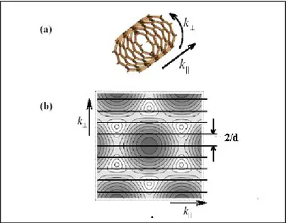
In a cylinder such as a CNT, the electron wave number perpendicular to the cylinder’s axial direction, k┴, is quantized. This quantization, together with the properties of graphene, lead us to a description of CNTs electronic structure.
The quantized k┴ are determined by the boundary condition:
π d k┴=2πj (1.9)
where j is an integer and d is the CNT diameter; A set of 1D energy dispersion relations is so obtained from Eq.1.8 by considering the small number of allowed wave vectors in the circumferential direction. The parallel lines in Fig. 5 represent the allowed k states in a CNT; each line is a different 1-D subband. In the direction parallel to the CNT axis, however, electrons are free to move over much larger distances and the electron wavenumber in the parallel direction, k||, is effectively continuous.
Figure 5 Quantization of wave states around a grapheme cylinder. A) The parallel and perpendicular axes of a CNT. B) Contour plot of graphene valence states for a CNT with the chiral angle θ = 0˚. The parallel lines spaced 2/d indicate the k vectors that are allowed by the cylindrical boundary condition. Each line is a 1-D subband. Lower energies are coloured darker. The circular contours around six K points are coloured white. The hexagonal formed by the six K points defines the graphene unit cell in k-space.
The continuum of k|| states in each k wrapping mode are called one-dimensional (1-D) subbands. These subbands are called Van-Hove singularities (vHSs) and are shown in fig.6 for a (9,0) and (10,0) SWNTs. The exact alignment between allowed k values and the K points of graphene is critical in determining the electrical properties of a CNT. Therefore the tube is metallic, if the
allowed states of nanotubes contains the graphite K points, otherwise is semiconducting. For example, in all armchair tubes the band with n1=n2 includes the K points, they are always metallic.
Fig.6 Electronic 1D density of states per unit cell for a (9,0) and (10,0) zigzag nanotube. Dotted lines correspond to the density of states of a 2D graphene sheet
.
The density of states near the Fermi level located at E = 0 is zero for the semiconducting (10, 0) nanotube and is non-zero for the metallic (9, 0)nanotube. From ref. [52].More deeply because of the degeneracy point between the conduction and valence bands, all the armchair tubes will exhibit metallic conduction at finite temperature, because only infinitesimal excitations are needed to excite carriers into the conduction band. The armchair tubes are thus a zero-gap semiconductor , just like a 2D graphene sheet. In general the tubes with chiral index (n1, n2)such that (n1, n2)/3 is integer, are metallic. Density of states measurements by scanning tunnelling spectroscopy (STS) confirm that some nanotubes (about 1/3) are conducting, yet most (about 2/3) are semiconducting [53,43]. Measurements confirm that the band gap is proportional to 1/d.
As reported above, by cutting the two dimensional band structure of graphene with j lines of length 2π/a (first Brillouin zone) and distance 2/d parallel to the direction of the tube axis (fig.7) it is possible to obtain the electronic properties of CNTs. This approach is called zone folding and is commonly used in nanotube and nanostructure research. The zone folding procedure neglects any effect of the cylinder geometry and curvature of the tube walls. The zone folding approach to calculate the electronic band structure of CNT falls down for small nanotube diameter (d<1nm) because in small diameter CNTs the mixing and the rehybridization of the p and s orbitals in the
curved graphite sheet can significantly change the electronic band structure [54]. For example, the (5,0) tube is metallic in contrast to what is expected from zone folding [55].
(3,3) (4,2)
Fig.7 Schematization of the zone folding approach to illustrate the electronic band structure of SWNT (3,3) left and (4,2). The two dimensional band structure of graphene has cutted with j lines of length 2π/a (first Brillouin zone) and distance 2/d parallel to the direction of the tube axis.
Vibrational properties
The phonon dispersion of a SWNT can be calculated by folding the phonon dispersion curves of a two-dimensional graphene layer analogous as for the case of the 2D electronic states. There are 2N carbon atoms in the unit cell of a carbon nanotube; therefore we have 6N phonon dispersion relations [56]. This model is applicable for almost all phonon modes but at low frequencies it does not always give the correct dispersion relation. Calculated phonon densities of states of a (10, 10) nanotube and a 2D graphene sheet are shown in Fig. 8. They were calculated by solving the three-dimensional carbon nanotube dynamic matrix [56].
One difference between the phonon density of states of a graphene sheet and a nanotube appears in the small peaks due to Van Hove singularities at low energy (~200 cm-1).
3D graphite has 6 normal phonon modes. The irreducible representation is given by [57]:
g u u g E A B E2 2 2 2 2 (1.10)
The phonon dispersion relation of 3D graphite is similar to that of a 2D graphene sheet due to the week interplanar coupling in graphite [58].
Fig.8 2D phonon dispersion relation (a) of a (10,10) armchair tube (left) and of a 2D graphene sheet (right) and the corresponding density of states (b) [56].
1.4
Aim of thesis
Techniques have been developed to produce nanotubes in sizeable quantities, but their cost still prohibits any large scale use of them. However, these naturally varieties are highly irregular in size and quality, and the high degree of uniformity necessary to meet the needs of research and industry is impossible in such an uncontrolled environment. There are several methods employed to make nanotubes, such as arc discharge, laser ablation, and chemical vapor deposition (CVD) . The best method to grow CNTs depends on their applications. In general, the CVD method has shown the most promise in being able to produce larger quantities of nanotube (compared to the other methods) at lower cost. But on the other hand CNTs grown by CVD are mixed with metallic catalyst particles and their wall have less graphitization (more defects) than CNTs produced by arc discharge where the temperature reaches more than 3000˚C to vaporizate the graphitic anode electrode. The first part of my work has been focused on the study of the best growth condition of CNTs by arc-discharge and CVD synthesis. To this aim an arc/discharge and a CVD apparatus were built up and subsequently the CNTs as grown were analysed and characterized by electronic microscopy, scanning probe microscopy and Raman spectroscopy (chapter 3 and chapter4).
The electronic properties (chapter 5) were investigated by electron energy loss spectroscopy (EELS) comparing, firstly, the different way of packaging of single wall carbon nanotubes (SWCNTs) in the bundles (i.e.; parallel, braided, turned or twisted) and secondly the structural properties of single wall, multi wall carbon nanotubes (MWCNTs) and highly oriented pyrolitic graphite (HOPG) obtained by the analysis of the extended energy loss fine structure (EXELFS) detected above the carbon K edge by using a transmission electron microscopy apparatus. The utilization of electrons as alternative source of X-rays for structural EXAFS-like spectroscopy is of paramount importance for a deeper understanding of the EXELFS spectra providing that the dipole approximation is still valid as well as the data analysis procedure.
Great interest for future applications of carbon nanotubes is the molecular optoelectronic.
Since their discovery by Ijiima [1,2], it has been done an enormous effort to functionalize both the end of the nanotubes and the walls, in order to modify their intrinsic properties. A further evolution for new nanotube-based devices is the functionalization by doping (59) or by deposition on the nanotube walls of some organic or inorganic compounds (60). This functionalization would allow the preparation of nanometric devices, in particular sensors, whose characteristics depend on the
bonded compound. Several papers have been already published on the application of functionalized carbon nanotubes, mainly for gas sensors (61) and biosensors (62).
The covalent functionalization of the walls can modify the properties of absorption of the nanotube destroying the extended lattice of pi bonds of the nanotubes (63). Therefore it is important to consider non covalent bonds not interact too much with the walls of the nanotubes. Porphyrins are strongly absorbed to HOPG graphite (Highly Oriented Pyrolytic Graphite) giving rise to a well ordered lattice (64-65). Such composite materials are interesting from a technological point of view and they can be used as organic LED (Organic Ligth Emission Diode) and solar cells (66-68). With respect to the conventional photovoltaic systems silicon-based, where the semiconductor has both the role of ligth absorber and charge carrier, in such systems the two functions are separated. The light is absorbed by organic molecules, easily ionized by the visible frequency, that are anchored to the surface of the semiconductor nanostructure. The separation of the charges occurs at the interface through the injection of electrons photoinduced by the organic molecules in the conduction band of the nanostructure itself. The carriers are moved in the conduction band of the semiconductor towards to charge collector. These mechanisms resulted to give high efficiency values (up to 10%) in the conversion of the light into current.
The achievement of the above objectives entail the development of the following step processes : a) fabrication of carbon nanotubes with CVD (Chemical Vapor Deposition): set-up of an experimental chamber and investigation of the structural and electronic properties of the grown nanotubes through several experimental techniques,
b) study of the photocurrent properties of the carbon nanotubes,
c) fabrication of carbon nanotubes with CVD between two nanoelectrodes,
d) deposition of organic molecules and their assembling properties on the carbon nanotubes walls and study of their photocurrent answer.
Bibliography chapter 1
[1] H. W. Kroto, J. R. Heath, S. C. O’Brien, R. F. Curl, and R. E. Smalley, Nature 318, 162 (1985). [2] S. Iijima, Nature 354, 56 (1991).
[3] S. Iijima and T. Ichihasi, Nature 363,603 (1993).
[4] D. S. Bethune, C. H. Kiang, M. S. deVries, G. Gorman, R. Savoy, J. Vazques, and R. Beyers, Nature 363, 605 (1993).
[5] W. Kratschmer, L. D. Lamb, K. Fostiropoulos, and D. R. Huffman, Nature 347, 354 (2000). [6] M. Radosavljevic, J. Lefebvre, and A. T. Johnson, Phys. Rev. B 64, 241307 (2001).
[7] S.B. Lee, K. B. K. Teo, L. A. W. Robinson, A. S. Teh, M. Chhowalla,et al., J. Vac. Sci. Technol. B 20, 2773 (2002).
[8] J.P. Salvetat, G. A. D. Briggs, J.M. Bonard, R. R. Bacsa, A. J. Kulik, et al., Phys. Rev. Lett. 82, 944 (1999).
[9] M. M. J. Treacy, T. W. Ebbesen, and J. M. Gibson, Nature 381, 678 (1996).
[10] A. Kis, G. Csanyi, J.P. Salvetat, T.N. Lee, E. Couteau, et al., Nature Materials 3, 153 (2004). [11] C. Zhou, J. Kong, E. Yenilmez, and H. Dai, Science 290, 1552 (2000).
[12] S. J. Tans, A. R. M. Verschueren, and C. Dekker, Nature (London) 393,49 (1998). [13] R. Martel, T. Schmidt, H. R. Shea, T. Hertel, and P. Avouris, Appl. Phys. Lett. 73, 2447 (1998).
[14] C. Zhou, J. Kong, and H. Dai, Appl. Phys. Lett. 76, 1597 (2000).
[15] S. J. Tans, M. H. Devoret, H. J. Dai, A. Thess, R. E. Smalley, L. J. Geerligs, and C. Dekker, Nature (London) 386, 474 (1997).
[16] M. Bockrath, D. H. Cobden, and P. L. McEuen, Science 275, 1922(1997).
[17] H. J. Dai, J. H. Hafner, A. G. Rinzler, D. T. Colbert, and R. E. Smalley, Nature 384, 147 (1996).
[18] S. S. Wong, J. D. Harper, P. T. Lansbury, and C. M. Lieber, J. Am. Chem. Soc. 120, 603 (1998).
[19] J. H. Hafner, C. L. Cheung, and C. M. Lieber, Nature 398, 761 (1999). [20]W. A. de Heer, A. Chatelain, and D. Ugarte, Science 270, 1179 (1995).
[21] A. G. Rinzler, J. H. Hafner, P. Nikolaev, L. Lou, S. G. Kim, D. Tomanek, P. Nordlander, D. T. Colbert, and R. E. Smalley, Science 269, 1550 (1995).
[ 22] J. Kong, N. R. Franklin, C. Zhou, M. G. Chapline, S. Peng, K. Cho, and H. Dai, Science 287, 622 (2000).
[23] P. Avouris, Acc. Chem. Res. 35, 1026 (2002).
[24] A. Bachtold, P. Hadley, T. Nakanishi, and C. Dekker, Science 294, 1317 (2001).
[26] A. M. Fennimore, T. D. Yuzvinsky, W.-Q. Han, M. S. Fuhrer, J. Cumings, and A. Zettl, Nature 424, 408 (2003).
[27] T. W. Odom, J. L. Huang, P. Kim, and C. M. Lieber, Nature 391, 62 (1998).
[28] P. Kim, T. W. Odom, J.-L. Huang, and C. M. Lieber, Phys. Rev. Lett. 82, 1225 (1999).
[29] L. C. Venema, J. W. Janssen, M. R. Buitelaar, J. W. G. Wild¨oer, S. G. Lemay, L. P.Kouwenhoven, and C. Dekker, Phys. Rev. B 62, 5238 (2000).
[30] M. Bockrath, D. H. Cobden, J. Lu, A. G. Rinzler, R. E. Smalley, L. Balents, and P. L.McEuen, Nature 397, 598 (1999).
[31] R. Egger, A. Bachtold, M. Fuhrer, M. Bockrath, D. Cobden, and P. McEuen, in Interacting Electrons in Nanostructures, edited by R. Haug and H. Schoeller (Springer, Berlin, 2001), vol. 579. [32] S. Frank, P. Poncharal, Z. L. Wang, and W. A. de Heer, Science 280, 1744 (1998).
[33] J. Nygard, D. Cobden, M. Bockrath, P. McEuen, and P. Lindelof, Appl. Phys. A Mater. Sci. & Process. A69, 297 (1999).
[34]Z. Yao, C. Dekker, and P. Avouris, “Electrical transport through single-wall carbon nanotubes”, in Carbon Nanotubes, edited by M. S. Dresselhaus, G. Dresselhaus, and P. Avouris (Springer, Berlin, 2001), vol. 80 of Topics in Applied Physics, p. 146.
[35] A. R. Goni, L. N. Pfeiffer, K. W. West, A. Pinczuk, H. U. Baranger, and H. L. Stormer, Appl. Phys.Lett. 61, 1956 (1992).
[36] O. M. Auslaender, A. Yacoby, R. de Picciotto, K. W. Baldwin, L. N. Pfeiffer, and K.W.West, Science 295, 825 (2002).
[37] A. M. Chang, Rev. Mod.Phys. 75, 1449 (2003).
[38] M.S. Dresselhaus, G. Dresselhaus & P. Eklund, ‘‘The science of fullerenes and carbon nanotubes’’, Academic (1996).
[39] R.A. Jishi, M. S. Dresselhaus, and G. Dresselhaus. Phys. Rev. B, 47, 16671 (1993). [40] C. Qin and L.-M. Peng, Phys. Rev. B 65, 155 431 (2002).
[41] Z. Zhang and C. M. Lieber, Appl. Phys. Lett. 62, 2792 (1993). [42] M. Ge and K. Sattler, Science 260, 515 (1993).
[43] J.W.G.Wildöer, L.C.Venema, A.G.Rinzler, R.E.Smalley, and C.Dekker, Nature 391, 59 (1998).
[44] T. W. Odom, J. H. Hafner, and C. M. Lieber, “Scanning probe microscopy studies of carbon nanotubes”, in Carbon Nanotubes, edited by M. S. Dresselhaus, G. Dresselhaus and P. Avouris (Springer, Berlin, 2001), vol. 80 of Topics in Applied Physics, p. 173.
[45] A. Hassanien, M. Tokumoto, S. Oshima, Y. Kuriki, F. Ikazaki, K. Uchida, and M. Yumura, Appl. Phys. Lett. 75, 2755 (1999).
[46] J. Muster, M. Burghard, S. Roth, G. S. Duesberg, E. Hernandez, and A. Rubio, J. Vac. Sci. Technol. B 16, 2796 (1998).
[47] X. B. Zhang, X. F. Zhang, S. Amelinckx, G. Van Tendeloo, and J. Van Landuyt, Ultramicroscopy 54, 237 (1994).
[48] L. C. Qin, T. Ichihashi, and S. Iijima, Ultramicroscopy 67, 181 (1997). [49] A. A. Lucas, F. Moreau, and P. Lambin, Rev. Mod. Phys. 74, 1 (2002).
[50] M. Gao, J. M. Zuo, R. D. Twesten, I. Petrov, L. A. Nagahara, and R. Zhang, Appl. Phys. Lett. 82, 2703 (2003).
[51] P.R.Wallace, Phys. Rev. 71, 622 (1947).
[52] R. Saito, M. Fujita, G. Dresselhaus, M.S. Dresselhaus, Appl. Phys. Lett.60, 2204 (1992). [53] C.H. Olk, J.P. Heremans, J. Mater. Res. 9, 259 (1994).
[54] X. Blase, L. X. Benedict, E. L. Shirley, and S. G. Louie, Phys. Rev. Lett. 72, 1878 (1994). [55] M. Machon, S. Reich, C. Thomsen, D. Sanchez-Portal, and P. Ordejon, Phys. Rev. B 66, 155410 (2002).
[56] R. Saito, G. Dresselhaus, M.S. Dresselhaus, Physical properties of Carbon Nanotubes, Imperial College Press (London) 1998.
[57] T.W. Ebbesen, Carbon Nanotubes, Edited by T.W. Ebbesen, CRC Press(Boca Raton, New York, London, Tokyo) 1997, Chapter I.
[58] P.C. Eklund, J.M. Holden, R.A. Jishi, Carbon 33, 959 (1995).
[59] S.B. Fagan, A.R.J. da Silva, R. Mota, R.J. Baierle, A. Razzio, Phys. Rev. B 67 033405(2003). [60] M. Strano, C.A. Dyke, M.L. Usrey, P.W. Barone, M.J. Allen, H. Shan, C. Kittrel, R.H. Hauge, J.M. Tour, R.E. Smalley, Science 301 1519 (2003).
[61] P. Qi, O. Vermesh, M. Grecu, A. Javey, Q. Wang, H. Dai, S. Peng, K.J. Cho, Nano Lett. 3 347 (2003).
[62] M. Shim, N.W.S. Kam, R.J. Chen, Y. Li, and H. Dai, Nano Lett. 2 285(2002). [63] J.Chen et al. Science 282, 95 (1998).
[64] Lei, S.B. Y., S.X.; Wang, C.; Wan, L.J.; Bai, C.L. J. Phys. Chem. B. 108, 224 (2004).
[65] Qiu, X. W., C.; Zeng, Q.; Xu, B.; Yin, S.; Wang, H.; Xu, S.; Bai, C. J. Am. Chem. Soc. 122, 5550 (2000).
[66] Coleman, J. N. et al. Synthetic Metals 102, 1174 (1999).
[67] Kymakis, E. & Amaratunga, G. A. Appl. Phys. Lett. 80, 112 (2002). [68] C.C.Wamser, H.S.Kim, J. K.Lee, Optical Materials 21, 221 (2002).
CHAPTER 2
Synthesis and Characterization of Carbon Nanotubes
2.1 Synthesis methods
Carbon nanotubes are fullerene-related structures which consist of graphene cylinders closed at either end with caps containing pentagonal rings. They were discovered in 1991 by the Japanese electron microscopist Sumio Iijima who was studying the material deposited on the cathode during the arc-evaporation synthesis of fullerenes [1]. He found that the central core of the cathodic deposit contained a variety of closed graphitic structures including nanoparticles and nanotubes, of a type which had never previously been observed. A short time later, Thomas Ebbesen and Pulickel Ajayan, from Iijima's lab, showed how nanotubes could be produced in bulk quantities by varying the arc-evaporation conditions [2]. These nanotubes typically have diameters around 5-30 nm and lengths around 10 micron. This paved the way to an explosion of research into the physical and chemical properties of carbon nanotubes in laboratories all over the world. A major event in the development of carbon nanotubes was the synthesis in 1993 of single-layer nanotubes. The standard arc-evaporation method produces only multilayered tubes. Iijima’s group [3], as well as Bethune and his collegues [4] found that addition of metals such as cobalt to the graphite electrodes resulted in extremely fine tube with single-layer walls. However, the yield of carbon nanotubes was low, and there were large amounts of metal carbide clusters and amorphous carbon attached to the nanotubes. This was a significant disadvantage of the arc-discharge method for further investigations on nanotubes, until 1997, when Journet and his co-workers found that the mixture 1 at.% Y and 4.2 at. % Ni as catalysts in graphite powder gave a high yield of 70-90% in their setup.[5] Another milestone in the synthesis of single-walled carbon nanotubes is the effort made by Smalley’s group in 1996[6]. He and his co-workers at Rice University developed a laser ablation technique that could grow single-walled carbon nanotubes with a relatively high yield of more than 70%, which paved the way for the take-off of investigations on the physical properties of SWNTs. They used the laser ablation on graphite rods doped with a mixture of cobalt and nickel powder in the inertial gas environment followed by heat treatment in vacuum to sublime out C. The nanotubes they got
had highly uniform diameters and bundled together as “ropes” by van der Waals interaction [6]. A purification process involving refluxing the as-grown nanotubes in a nitric acid for an extended period of time was also developed by Smalley and his co-workers [7]. This method has been widely applied to remove amorphous carbon and residual catalytic metal particles commonly found mixed with nanotubes in the final product. In spite of the success of the arc-discharge and laser ablation methods in producing carbon nanotubes with a high yield, the final products are usually bundled nanotubes decorated with catalyst particles and amorphous carbon. Previous studies using such products have been severely hampered by the lack of control over the nanotube growth and the difficulty in wiring up individual nanotube devices, making practical applications almost impossible. It would be desirable to have a high-yield synthesis route to produce SWNTs with controlled length, positions, and orientations for both scientific and technological studies. It is equally desirable to develop a method to make robust, low-resistance electrical contacts between nanotubes and metallic electrodes. These goals pose great challenges to nanotube synthesis, processing, and assembly strategies. Significant progress in addressing these challenges has been made by Dai and his co-workers: a novel CVD method was developed to grow high-quality individual single-walled carbon nanotubes off patterned catalyst islands directly on substrates [8-11]. This technique readily yields large numbers of SWNTs at specific locations, and opens up new possibilities for integrated nanotube systems. Significant progress has also been made by several other groups toward CVD growth of high-quality SWNTs. Liu and his co-workers have developed a way to produce Fe/Mo catalyst supported on alumina aerogel [12]. This catalyst possesses a high surface area and large mesopore volume, and has led to a nanotube catalyst ratio as high as 2 :1 in the CVD product using methane as the feedstock. Smalley and his co-workers have developed a gas-phase CVD process to grow bulk quantities of single-walled carbon nanotubes [13], where carbon monoxide is used as the feedstock and catalytic nanoparticles are generated in situ by thermal decomposition of an iron-containing compound. Bulk production of SWNTs has also been successfully achieved by other groups using CVD techniques [14, 15]. In addition to the CVD synthesis of SWNTs, by using different hydrocarbon gases, catalysts, flowing conditions, and temperatures, multiwall carbon nanotubes (MWNTs) can also be synthesized. In contrast to the arc-discharge or laser ablation techniques, CVD growth of MWNTs can give us aligned and ordered nanotube structures. The typical methods of growing aligned multiwalled nanotube structures have been developed by several groups independently. For example, Xie and his co-workers used iron oxide particles created in the porous silica as the catalyst and 9% acetylene in nitrogen as the carbon feedstock [16, 17], while Ren and his co-workers developed a method to grow oriented MWNTs on glass substrates by a plasma-assisted CVD method with nickel as the catalyst and acetylene as the
carbon source [18]. In addition to the well-developed CVD method, several novel synthesis techniques have been demonstrated. In 1998, Tang et al. found that pyrolysis of tripropylamine can form mono-sized SWNTs [19]. The diameter of the SWNT grown this way can be as small as 4 Å, close to the theoretical limit. They have also successfully observed superconductivity with their SWNT samples with a transition temperature of 15 K [20]. Schlittler and his co-workers developed a technique to control the chirality of the SWNT [21]. They deposited Ni and C60 layers alternately in a sandwich manner on a Mo substrate, and then heated the sample to high temperature in vacuum while applying a magnetic field oriented parallel to the surface normal. Their procedure produces carbon nanotubes with identical chiralities.
Fig.1(left) The transmission electron microscope (TEM) image of the first discovered carbon nanotubes by Iijima: the multiwalled carbon nanotubes was found in the soot of an arc-discharge setup. Image taken from [1].
Fig.2(right) Bundles of SWNTs. Image taken from [5].
As mentioned above carbon nanotubes are generally produced by three main techniques, arc discharge, laser ablation and chemical vapour deposition. The most widely used technique to produce nanotubes is the arc discharge evaporation method [22,23,24] also used for fullerene synthesis [25]. An electric arc discharge is produced between two carbon electrodes in an inert helium or argon atmosphere. The temperature of > 3000°C between the electrodes is high enough to sublime the carbon.
A second approach is the laser ablation method [26]. A piece of graphite is vaporised by laser irradiation in an inert gas. With the arc discharge and the laser ablation method both SWNT and MWNT can be produced. MWNT are synthesised with pure graphite; for SWNT however, metal particles are required. In the arc discharge method a drilled carbon rod is filled with a metal powder
(Ni, Co, Pt, Cu, Co/Ni, Co/Pt, Fe/Ni…), and in the laser ablation method a transition-metal/graphite composite is used. These synthesis methods have both the advantage to produce high quality nanotubes. A disadvantage of the vaporisation methods is the high temperature (> 3000°C) required, this limits a scale-up of the processes. Furthermore, the diverse by-products e.g. amorphous carbon and diverse nanoparticles have to be removed by subsequent purification [27]. A more efficient approach to the nanotube synthesis without the above mentioned drawbacks is the CVD method [28], earlier used for the synthesis of carbon filaments. In this method a carbon-containing gas or vapor (C2H2, CH4, CO, pentane…) is dissociated over supported metal clusters at 500 to 1200°C for some minutes up to several hours. The metal clusters on the substrate serve as nucleation centres for the nanotube growth. It is suggested that for the carbon filament as well as for the nanotube growth the carbon-containing gas decomposes on the metal surface and that the carbon diffuses from one side through the metal particle and precipitates on the other side [29]. The CVD method has the advantage to produce lower quantities of by-products. The graphitization degree of such nanotubes as compared to those produced by arc discharge or laser ablation [23] is lower because of the lower synthesis temperatures.
In Table 1, is given a short summary of the three most common techniques used nowadays with their efficiency.
Method Arc discharge method
Chemical
vapour deposition (CVD) Laser ablation
Who Ebbesen and Ajayan, NEC, Japan 1992 2
Endo, Shinshu University, Nagano, Japan 30
Smalley, Rice, 19956
How
Connect two graphite rods to a power supply, place them a few millimetres apart, and throw the switch. At 100 amps, carbon vaporises and forms a hot plasma.
Place substrate in oven, heat to 600 oC, and slowly add a
carbon-bearing gas such as methane. As gas decomposes it frees up carbon atoms, which recombine in the form of NTs
Blast graphite with intense laser pulses; use the laser pulses rather than electricity to generate carbon gas from which the NTs form; try various conditions until hit on one that produces prodigious amounts of SWNTs
Typical yield
30 to 90% 20 to 100 % Up to 70%
SWNT
Short tubes with diameters of 0.6 - 1.4 nm
Long tubes with diameters ranging from 0.6-4 nm
Long bundles of tubes (5-20 microns), with individual diameter from 1-2 nm.
M-WNT Short tubes with inner diameterof 1-3 nm and outer diameter of approximately 10 nm
Long tubes with diameter ranging from 10-240 nm
Not very much interest in this technique, as it is too expensive, but MWNT synthesis is possible.
Method Arc discharge method
Chemical
vapour deposition (CVD) Laser ablation
structural defects; MWNTs without catalyst, not too expensive, open air synthesis possible
process, SWNT diameter controllable, quite pure.
The reaction product is quite pure.
Con Tubes tend to be short with random sizes and directions; often needs a lot of purification
NTs are usually mixed with the catalyst particle. Often riddled with defects
Costly technique, because it requires expensive lasers and high power requirement, but is improving
2.2 Spectroscopic characterization
2.2.1 Raman Spectroscopy
Phonons are the quasi-particles that describe the quantized lattice vibrations or normal modes of a crystal. The crystal possesses 3N phonon branches where N is the number of atoms in the unit cell. A three-dimensional crystal has three acoustic modes with zero frequency at the G point, corresponding to uniform displacements of the crystal. All remaining branches, where the atoms in the unit cell move out-of-phase, are referred to as optical phonons, since in polar crystals they can directly couple to light [34]. Phonons are bosons and contribute the major part to the heat capacity of a crystal. They play an important role for both transport and optical properties, because they are main path by which excited electrons or other quasi-particles can decay into lower energy states. In fact, in an ideal crystal at finite temperature phonons are the only source of electrical resistance. Information on the properties of the phonons can be obtained from direct absorption of light by phonons (infrared spectroscopy, for carbon nanotubes see Ref. [35, 36]), measurements of the specific heat and the phonon density of states [37–39], Raman scattering or from transport experiments. In principle, the phonon dispersion of a crystal can be measured by inelastic scattering of neutrons, electrons, or X-ray photons. For these experiments, a minimum size of a single crystal is required, which is not available from carbon nanotubes at present. The closest experimental approximation to the phonon dispersion of carbon nanotubes is therefore the in-plane phonon dispersion of graphite.
Even in graphite the phonon dispersion was not known from experiments, because the standard method of inelastic neutron scattered requires single crystals on the order of cm in size, which do
not exist. For the novel method of inelastic X-ray scattering, on the other hand, single crystals ~ 100 µm are sufficient.
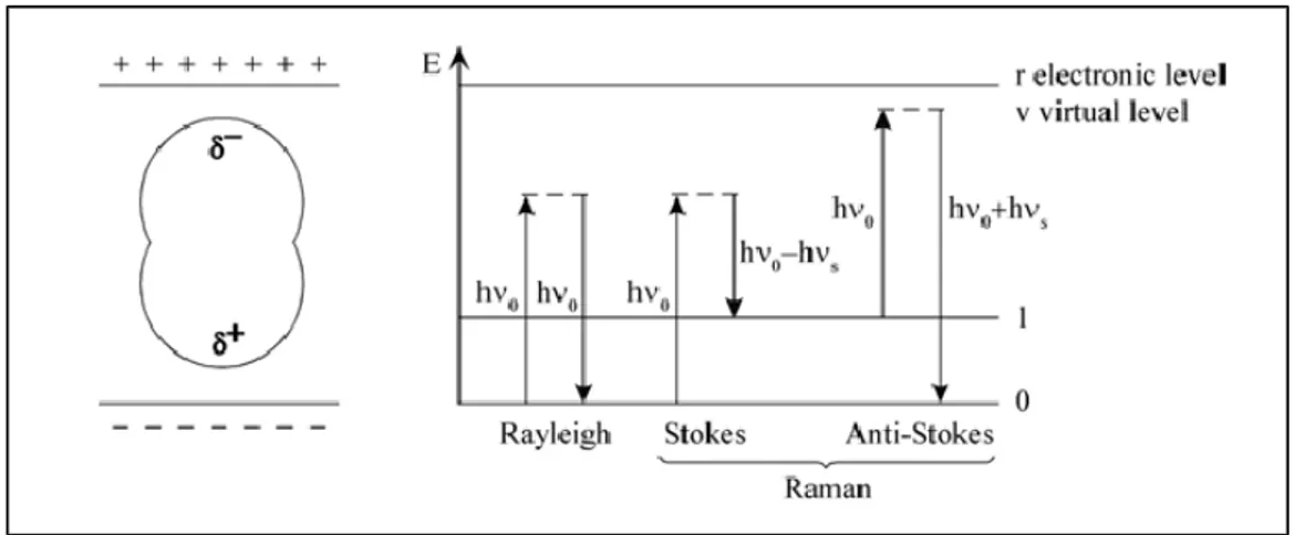
If a light quantum hν0 hits a molecule it is scattered with a high probability elastically with the energy hν0 in the so-called Rayleigh scattering process (fig.3). With a much lower probability (~10 -5) it is scattered inelastically with an energy hν
0±hνs in the Raman scattering process in which thevibrational energy hνs is exchanged. According to the Botzmann’s law most molecules are in their vibrational ground state at ambient temperature. Therefore the Raman process that transfers energy to the molecule and leaves a quantum with lower energy hν0-hνs has a higher probability
than the reverse process. The corresponding Raman lines are called Stokes and anti-Stokes lines, respectively [40].
Fig. 3: Polarized molecule in an electric field (left), energy diagram of the different light scattering processes. The elastic Rayleigh scattering and the inelastic Raman scattering (Stokes/Anti-Stokes) (right)
In the classical theory the Raman scattering is explained as follows: if a diatomic molecule is irradiated with an alternative electric field E:
E(t)= E0cos(2v0t)
(2.4)
an electric dipole moment P is induced:
where α is the polarisability (in general a tensor). If the molecule vibrates with a frequency νs, the nuclear displacement is written as:
) 2 cos( 0 v t q q s (2.6)
For a small amplitude variation, α is a linear function of q:
.. 0 0 q q (2.7)
where α0 corresponds to the polarisability at the equilibrium position. By combining the equations we get [41]: P= α0E0 0 0 0 2 1 ) 2 cos( q q t v E0
cos
2
v
0
v
s
t
cos
2
v
0
v
s
t
(2.8)The first term corresponds to an oscillation of a dipole with frequency v0 (Rayleigh
scattering), the second term and the third term corresponds to the Raman scattering with frequency
s
v
v0 (anti-Stokes) and v0 vs (Stokes). A vibration is only Raman active when
0 q is not zero. The classical equation does not describe the intensities of the Stokes and anti-Stokes lines. The intensity ratio of the anti-Stokes and Stokes of a Raman active vibration is given by vs is given
by [42]: 1 4 0 0 exp KT hcv v v v v I I I s s s Stokes Stokes anti
(2.9)
where T is the specimen temperature.
For crystals the polarizability α is replaced by the susceptibility tensor χ:
Whether a vibration is Raman active or not is determined by the symmetry of the crystal described in group theory. When the frequency of the incident radiation approaches an electronic transition frequency (electronic r level fig.3) the intensity of the Raman bands is strongly enhanced.
Raman spectra obtained with exciting laser frequencies close to absorption bands are called resonance Raman spectra.
For crystals transparent to the incident and scattered light the conservation of energy and momentum can be written as [43]:
s hv hv hv hv 0 1 (2.11) k =k0-k1=±qs (2.12)
where νs and qs are the frequency and wave vector of a crystal excitation. For typical light scattering
experiments in or near the visible the range of scattering wave vectors is 0k 106cm-1. For first-order scattering processes the accessible range |qs|, is small compared to a reciprocal lattice
vector. In high order processes the range of the individual wave vectors of the excitation can be from zero to a reciprocal lattice vector since k =
i qi.
In the following cases the wave vector conservation (2.12) breaks down:
1) The scattering medium has no translation symmetry i.e. in crystals with defects, solid solutions and in amorphous solids. The absence of translation symmetry allows scattering by modes with qs
k.2) The scattering volume is small. In this case light scattering is due to excitations with wave vectors in a rangeq2/d where d is a characteristic length in the scattering volume.
3) The incident and scattered waves are damped inside the scattering volume. Under this conditions (metals and small gap semiconductors that are opaque to the light) k0 and k1 are complex.
As discussed above the scattering efficiency gets larger when the laser energy matches the energy between optically allowed electronic transitions in the material. The resonance Raman intensity depends on the density of electronic
states (DOS) available for the optical transitions, and this property is very important for one-dimensional (1D) systems as SWNTs.
Because of a single wall carbon nantubes can be imagine as a graphene sheet rolled up into a cylinder, periodic boundary conditions in the radial direction have to be applied. The reciprocal wave vector is quantized, leading to a confinement of electrons in this direction. This phenomenon gives rise to spikes in the DOS, called van Hove singularities. Therefore, in practice, a single carbon nanotube exhibits a ‘molecular-like’ behaviour, with well defined electronic energy levels at each vHS.
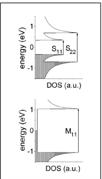
Figures 4 (a)–(c) show the DOS for three different SWNTs. The three DOS curves in figures 4 (a)– (c) come from different SWNTs as labelled by their (n1,n2) indices [44] (see caption). Each pair of indices defines a unique way to roll up the graphene sheet to form the nanotube, and each unique (n1, n2) nanotube has a distinct electron and phonon structure. An observable Raman signal from a carbon nanotube can be obtained when the laser excitation energy is equal to the energy separation between vHSs in the valence and conduction bands (e.g., see ES11, ES22 and EM11 in figure 4), but restricted to the selection rules for optically allowed electronic transitions [45]–[47]. Because of this resonance process, Raman spectra at the single nanotube level allow us to study the electronic and phonon structure of SWNTs in great detail. When Raman spectra of SWNT bundle samples are taken, only those SWNTs with Eii in resonance with the laser excitation energy will contribute strongly to the spectrum [48].
Fig.4 DOS for a) armchair (10,10) SWNT, b) chiral (11,9) SWNT and c) zigzag (22,0) SWNT obtained with the tight binding model d) shows the electronic transition energy Eii for all the
(n1,n2) SWNTs with diameter from 0.4 and 3.0 nm using a simple first-neighbour tight binding
model. Distortion from this simple one-electron model is expected for the lower energy transition Es11 and for SWNTs with d less than 1nm. Image taken from[48].
In fig.5 is shown a schematic representation of Raman features for SWNTs of diameter ~1nm :
- RBM region (up to 400 cm-1): it describes phonon modes where all atoms move in phase in the radial direction (fig.6 left). RBM frequency is a finger print of the presence of SWCNTs, it is approximately proportional to the inverse tube diameter and is therefore frequently used for diameter determination.
- “D-band” (D as Disorder) at ~1350 cm-1: the intensity of the D-band can be a measurement of the degree of graphitization of the sample. It is induced by the presence of defects and stems from inside the Brillouin zone.
- “G-band” (G for Graphite) at ~ 1580 cm-1: It is due to the Raman-allowed tangential mode (fig.6 right). Unlike graphite, the tangential G mode in SWNTs gives rise to a multi-peak feature, also named the G band, where up to six Raman peaks can be observed in a first-order Raman process.
Fig.5 Schematic representation of Raman spectra of SWNTs where are indicated: the RBM region (until 400 cm-1), the D and G bands peaked
Fig.6 Schematic representation of the Radial Breathing Mode (left) and the tangential modes (right). G- is indicated for tangential modes with atomic displacement along the
circumferential direction while G+ is indicated for atomic displacements along the tube axis.
2.2.2 Electron Energy Loss Spectroscopy (EELS)
Electron Energy Loss Spectroscopy (EELS) concerns the analysis of energy spreading of initially almost monoenergetic electrons, after their interaction with the sample. The technique is frequently used in association with Transmission Electron Microscopy (TEM) and interaction takes place inside the specimen. Measuring the energy distribution of electrons that have passed through a thin specimen can be obtained informations about its structure. The spectral energy resolution is largely determined by the energy width of the electron source: 1 - 2 eV for a thermionic source, 0.5 to 0.7 eV for a field-emission gun and 0.1 - 0.2 eV for a FEG (Field Emission Gun) followed by a monochromator [49].
The electrons impinging on the sample may lose energy by a variety of mechanisms. These losses can reveal the composition of the sample in TEM.
-Plasmon losses are a frequent cause of energy loss. Plasmons are collective excitations of the electron gas in the material and are typically several electron Volts in magnitude (5-30 eV).
-Phonon losses can also occur, which are much smaller (less than 0.1 eV), and the energy spread of the monoenergetic beam must be particularly small to detect such losses. Phonons are quantized sound waves within the solid.
A typical energy loss spectrum is divided in two regions at low and at high energy. Low Energy Loss:
For very thin specimens, the most prominent feature is the zero-loss peak that is due to unscattered electrons that are transmitted without any interaction with the specimen. (area I0 , representing purely elastic scattering, see fig.7). The second contribution includes the plasmon peak, due to inelastic scattering by outer-shell (valence) electrons in the specimen, it is centred around a plasmon energy Ep, generally in the range 10-30 eV. Plural scattering of the transmitted electrons gives rise to additional peaks, at multiples of Ep.
The plasmon losses just mentioned are called “volume plasmons” because they arise from the interaction with the electrons in the bulk of the specimen. The incident electrons, however, can also originate a longitudinal wave of charge density which travels along the surface and is referred to as “surface plasmon”. In the simplest situation, the vacuum-metal interface, the energy Es of the surface plasmon peak in the low-loss spectrum is:
Es=Ep/√2 (2.13) while, in the slightly more general case, dielectric-metal interface (2.13) becomes:
Es=Ep/√ (1+ε1) (2.14) where ε1 is the real part of the dielectric function. Generally surface plasmons have about half the energy of bulk plasmon and their peak are much less intense than the volume plasmon peak, even in the thinnest specimen.
High Energy Loss:
At higher energy loss, ionization edges occur due to inelastic excitation of inner-shell (core) electrons. They are superimposed on a falling background representing the tail of lower-loss inelastic processes, which usually approximates to a power law:
background~AE-r (2.15)
where A and r are constants within a limited range of energy loss E . The threshold energy of each edge is the binding energy of the corresponding atomic shell and is tabulated for all elements and electron shells (K, L, M, etc.), allowing elements present in the specimen to be identified. The
energy-loss spectrum also contains fine structure, in the form of intensity oscillations or local peaks.
Extended energy-loss fine structure (EXELFS) have a weaker intensity modulation starting at 50 eV or more from the ionization edge and can be analyzed to give the distance of nearest-neighbour atoms.
Fig. 7 (a) Low-loss spectrum and (b) the core-loss region showing several basic shapes of ionization edge, each superimposed on a spectral background (dashed curves). Image taken from [50].
2.2.3 Extended Electron Energy Loss Fine Structure
(EXELFS)
The energy-loss spectrum also contains fine structure, in the form of intensity oscillations or local peaks. Extended energy-loss fine structure (EXELFS) have a weaker intensity modulation starting at 50 eV or more from the ionization edge and can be analyzed to give the distance of nearest-neighbour atoms . In particular EXELFS, probing the unoccupied electron states above Fermi level in the energy range of core edge levels, can give information similar to those provided by XAS (X-ray absorption spectroscopy). When an X-ray passes through a material, it attenuates progressively and undergoes some discontinuities for energies corresponding to electronic transitions of core electrons towards unoccupied states above the Fermi level. In the case of crystalline solid, the atoms excited by the X-ray emit a photoelectron described by spherical outgoing wave centred on the atomic target. The emitted photoelectron is retrodiffused by the electrons of the nearest neighbour atoms. This
retrodiffusion is represented by spherical waves centred on the sites of neighbouring atoms. A portion of this waves interferes with the first outgoing waves and it gives rise to a modulation of the absorption coefficient μ(ω). EXAFS reflects the local order, and the amplitude of the oscillations depends on the coordination number of neighbours Nj of type j located at a distance rj from the absorbing central atom. The phenomenology of the EXELFS process is similar to those related to the photoelectrons which generate the EXAFS features.
Fig.8 Schematic picture of EXAFS (a) and EXELFS (b) spectroscopies [51].
The exciting source is a beam of monoenergetic primary electrons that looses a discrete amount of energy at least equal to that one necessary to ionize a core electron in the medium. The energy distribution of these inelastic electrons shows the same features of X-ray absorption coefficient, as shown schematically in fig.8. The modulation observed in the x-ray absorption coefficient μ(E) corresponds to the features observed in the yield N(E) due to the transmitted electron from the solid sample. In the EXAFS spectroscopy the different final states of the excited core electron above Ef can be filled by varying the energy of the x-ray probe. In EXELFS spectroscopy the same features are detected in N(E) measuring different energy losses ΔE of the primary electron beam Ep which reflects the same final states of the core electron excited in the medium [52].
A rough evaluation of the scattering cross section can be made within the framework of the
Bor-approximation. In the limits of
1
a
rq
(dipole approximation) the N(E) distribution of the measured scattered electrons will be proportional to the cross section integrated between qmin and qmax of the momentum transferred, depending on the experimental scattering geometry [53,54]:( ) r 2log(qmax/qmin)
dE d E
N f q ai (2.16)
where εq is the unit versor in the direction of q vector and ra is the atomic radius of the core electron. The formula above is a first approximation, similar to that one of the X-ray absorption coefficient [55] according to the following equivalence:
2 ) ( :N E f q ra i EELFS (2.17) EXAFS:(E) f rai 2 (2.18)
where ε is the electric field in the direction of the X-ray polarization.
The utilizations of electrons as an alternative source of X-rays for structural EXAFS-like spectroscopy has been demonstrated for the first time by Ritsko et al.[56] and later by Kincaid et al. [57] for the K-edge of graphite and by Leapman et. al. [58] for heavier elements like chromium. The comparison of transmission energy loss spectra with EXAFS is of paramount importance for a deeper understanding of the EXELFS spectra, based on the same interference process which occurs above a core edge in the X-ray absorption coefficient.
The oscillatory behaviour of the absorption coefficient μ is described in the case of a K-edge by the following relation [59, 60]. dR k kR k F kR e R g k) ( ) R ( , )sin(2 ( )) ( 2 2/ 0 0
(2.19) where:- g(r) is the radial distribution function (Gaussian curve: 2 2k2
e )
-F(k) is the backscattering amplitude, -r is the inter-atomic distance
- k is the wave vector
- R
e 2 describes the inelastic diffusion of the photoelectron , where λ(k) is the mean free path of the emitted electron and
-(k) is the total phase shift.
In the standard EXAFS formalism a Gaussian pair distribution function g(r) is characterized by the Debye-Waller factor, σ, that takes account for the atomic thermal vibration around the equilibrium position [61, 62]. The EXAFS formula for the first shell becomes:
)) ( sin( ) ( ) (k A k 1 k (2.20)
where the amplitude and phase of the EXAFS are given by:
)exp( 2 ) ) ( 2 exp( ) ( ) ( ) ( 2 2 2 k k R k F kR k N k A (2.21) (k)2kR(k) (2.22)
where R is the mean inter-atomic distance.
The structural analysis is performed through Fourier Transform of the experimental signal χ(k), according to the following relation:
F R k e dk k k ikR
max min 2 ) ( 2 1 ) ( (2.23)F(R) curve shows peaks which are related to the different atomic shells at distance R(Ǻ) surrounding the absorbing atom located at the origin of the scale.
Finally we stress that the basic assumption underlying the validity of EXAFS formula is the neglect of multiple scattering events.
The general discussion about the scanning probe microscopy (AFM and STM) and the electron microscopy (SEM and TEM) characterizations are reported in appendix 2 [31, 32, 33].
Bibliography chapter 2
[1] S. IIjima, Nature 354, 56 (1991).
[2] T. W. Ebbesen and T. M. Ajayan, Nature 358, 220 (1992). [3] S. Iijima and T. Ichibashi, Nature 363, 603 (1993).
[4] D. S. Bethune, C. H. Kiang, M. S. Devries, G. Gorman, R. Savoy, J. Vazquez, and R. Beyers, Nature 363, 605 (1993).
[5] C. Journet, W. K. Maser, P. Bernier, A. Loiseau, M. L. de la Chapelle, S. Lefrant, P. Deniard, R. Lee and J. E. Fischer, Nature 388,756 (1997).
[6] A. Thess, R. Lee, P. Nikolaev, H. J. Dai, P. Petit, J. Robert, C. H. Xu, Y. H. Lee, S. G. Kim, A. G. Rinzler, D. T. Colbert, G. E. Scuseria, D. Tomanek, J. E. Fischer, and R. E. Smalley, Science 273,483 (1996).
[7] J. Liu, A. G. Rinzler, H. Dai, J. H. Hafner, R. K. Bradley, P. J. Boul, A. Lu, T. Iverson, K. Shelimov, C. B. Huffman, F. Rodriguez-Macias, Y. S. Shon, T. R. Lee, D. T. Colbert, and R. E. Smalley, Science 280, 1253 (1998).
[8] J. Kong, H. T. Soh, A. M. Cassell, C. F. Quate, and H. Dai, Nature 395, 878 (1998).
[9] J. Kong, C. Zhou, A. Morpurgo, H. T. Soh, C. F. Quate, C. Marcus, and H. Dai, Appl. Phys. A 69, 305 (1999).
[10] J. Kong, A. M. Cassell, and H. Dai, Chem. Phys. Lett. 292, 567 (1998). [11] A. Cassell, J. Raymarks, J. Kong, and H. Dai, J. Phys. Chem. 103,6484 (1999). [12] M. Su, B. Zheng, and J. Liu, Chem. Phys. Lett. 322, 321 (2000).
[13] P. Nikolaev, M. J. Bronikowski, R. K. Bradley, F. Rohmund, D. T. Colbert, K.A. Smith, and R.E. Smalley, Chem. Phys. Lett. 313,91 (1999).
[14] E. Flahaut, A. Govindaraj, A. Peigney, C. Laurent, and C. N. Rao, Chem. Phys. Lett. 300, 236 (1999).
[15] J. F. Colomer, C. Stephan, S. Lefrant, G. V. Tendeloo, I. Willems, Z. Kanya, A. Fonseca, C. Laurent, and J. B. Nagy, Chem. Phys. Lett. 317, 83 (2000).
[16] W. Z. Li, S. S. Xie, L. X. Qian, B. H. Chang, B. S. Zou, W. Y. Zhou, R. A. Zhao, and G. Wang, Science 274, 1701 (1996).
[17] Z. W. Pan, S. S. Xie, B. H. Chang, C. Y. Wang, L. Lu, W. Liu, W. Y. Zhou, W. Z. Li, and L. X. Qian, Nature 394, 631 (1996).
[18] Z. F. Ren, Z. P. Huang, J. W. Xu, J. H. Wang, P. Bush, M. P. Siegal, and P. N. Provencio, Science 282, 1105 (1998).
[19] Z. K. Tang, H. D. Sun, J. Wang, J. Chen, and G. Li, Appl. Phys. Lett. 73, 2287 (1998). [20] Z. K. Tang, L. Y. Zhang, N. Wang, X. X. Zhang, G. H. Wen, G. D. Li, J. N. Wang, C. T. Chan, and P. Sheng, Science 292, 2462 (2001).
[21] R. R. Schlittler, J. W. Seo, J. K. Gimzewski, C. Durkan, M. S. M. Saifullah, and M. E. Welland, Science 292, 1136 (2001).
[22] M. S. Dresselhaus, G. Dresselhaus, and P. C. Eklund, “Science of fullerenes and Carbon Nanotubes.” Academic Press, San Diego, 1996.
[23] S. J. Tans, A. R. M. Verschueren, and C. Dekker, Nature (London) 393,49 (1998). [24] R. Martel, T. Schmidt, H. R. Shea, T. Hertel, and P. Avouris, Appl. Phys. Lett. 73, 2447 (1998).
[25] C. Dekker, Physics Today 52, 22 (1999).
[26] C. Zhou, J. Kong, and H. Dai, Appl. Phys. Lett. 76, 1597 (2000).
[27] S. J. Tans, M. H. Devoret, H. J. Dai, A. Thess, R. E. Smalley, L. J. Geerligs, and C. Dekker, Nature (London) 386, 474 (1997).
[28] M. Bockrath, D. H. Cobden, and P. L. McEuen, Science 275, 1922(1997). [29] C. Zhou, J. Kong, E. Yenilmez, and H. Dai, Science 290, 1552 (2000).
[30] Endo, Morinobu, Takeuchi, Kenji, Igarashi, Susumu, Kobori, Kiyoharu, Shiraishi, Minoru, and Kroto,Harold W., Journal of Physics and Chemistry of Solids, 54, (12), 1993.
[31] H. Bethge, J. Heydenreich, Electron Microscopy in Solid State Physics, Elsevier (Amsterdam, Oxford, New York) 1987.
[32] D.B. Williams, C.B. Carter, Transmission Electron Microscopy; Basics , Plenum Press (New York, London), 1996.
[33] http://www.chem.qmw.ac.uk/surfaces/scc/scat5_3.htm.
[34] P. Y. Yu and M. Cardona, ‘’Fundamentals of Semiconductors’’ (Springer, Berlin, 1999, 2nded.).
[35] U. Kuhlmann, H. Jantoljak, N. Pfander, P. Bernier, C. Journet, and C. Thomsen, Chem. Phys. Lett. 294, 237(1998).
[36] U. Kuhlmann, H. Jantoljak, N. Pf¨ander, C. Journet, P. Bernier, and C. Thomsen, Synth. Met. 103, 2506 (1999).
[37] A. Mizel, L. X. Benedict, M. L. Cohen, S. G. Louie, A. Zettl, N. K. Budraa, and W. P. Beyermann, Phys. Rev. B 60, 3264 (1999).
[38] S. Rols, Z. Benes, E. Anglaret, J. L. Sauvajol, P. Papanek, et al., Phys. Rev. Lett. 85, 5222 (2000).
[39] K. B. J. C. Lasjaunias, Z. Benes, J. E. Fischer, and P. Monceau, Phys. Rev. B 65, 113 409 (2002).
[40] Infrared and Raman Spectroscopy, edited by B. Schrader, VCH. (Weinheim, New York, Basel, Cambridge, Tokyo), 1995.
[41] J.R. Ferraro, K. Nakamoto, Introductory Raman Spectroscopy, Academic Press (Boston, San Diego, New York, London, Sydney,Tokyo, Toronto) 1994.
[42] P.V. Huong, R. Cavagnat, Phys. Rev. B 51, 10048 (1995).
[43] Light Scattering in Solids I, edited by M. Cardona, Springer-Verlag (Berlin, Heidelberg, New York), 1983.
[44] Dresselhaus M S and Eklund P C 2000 Adv. Phys. 49 705. [45] Lin M F 2000 Phys. Rev. B 62 13153.
[46] Bozovic I, Bozovic N and Damnjanovic M 2000 Phys. Rev. B 62 6971.
[47] Gruneis A, Saito R, Samsonidze Ge G, Kimura T, PimentaMA, Jorio A, Souza Filho A G, Dresselhaus G and Dresselhaus M S 2003 Phys. Rev. B 67 165402.
[48] A Jorio, M A Pimenta, A G Souza Filho, R Saito,G Dresselhaus and M S Dresselhaus New Journal of Physics 5 (2003).
[49] R.F. Egerton, ‘Electron Energy-Loss Spectroscopy in the Electron Microscope’, 2nd edition,Plenum, New York, 1996.
[50] F. Hofer, in Microbeam Analysis - 1991, San Francisco Press, San Francisco, 1991; p. 255. [51] M.De Crescenzi and G. Chiarello, J. Phys. C 18 (1985) 3595; M. De Crescenzi Surf. Sci. Rep. 21, 89 (1995).
[52]M. De Crescenzi, L.Lozzi, P. Picozzi, S. Santucci, M. Benfatto and C.R. Natoli PRB 39,12 (1989).