Radiation hard design of HfO
2
based 1T1R cells
and memory arrays
Alessandro Grossi
∗, Cristiano Calligaro
†, Eduardo Perez
‡, Florian Teply
‡,
Thomas Mausolf
‡, Cristian Zambelli
∗, Piero Olivo
∗, and Christian Wenger
‡ ∗Universit`a di Ferrara, Dipartimento di Ingegneria, ENDIF, Via G. Saragat 1, 44122 Ferrara, Italy†RedCat Devices srl, via Moncucco 22, 20142 Milano, Italy ‡IHP, Im Technologiepark 25, 15236 Frankfurt (Oder), Germany
E-mail: [email protected]
Abstract—In this work the electrical performance of a
Rad-Hard designed 1T1R device based on the combination of an Enclosed Layout Transistor (ELT) and an TiN/HfO2/Ti/TiN
based resistor are presented for the first time. Moreover, an architectural solution for 1Mbit radiation hard RRAM array implementation is proposed.
I. INTRODUCTION
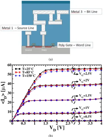
Semiconductor memories, among rad-hard integrated circuit scenario, are one of the most critical topics for space appli-cations. Actually both volatile and non-volatile memories, ex-cluding few exceptions, are integrated using standard processes and standard architectures. This means that the final device is typically at least Rad-tolerant and not Rad-Hard and failure during mission is avoided using Error Correcting Code tech-niques including redundancy at the board level. Since standard silicon memories, such as flash memories tend to fail under irradiation, a new approach is envisaged: the development of a specific memory technology, so called resistive random-access memory (RRAM). The switching effect of the RRAM devices is determined by the formation and modification of conductive filaments composed of oxygen vacancies, which are controlled through the motion of oxygen anions by an applied electric field [1]–[4]. The intrinsic radiation tolerance of RRAM significantly reduces sensitivity to radiation-induced bit upsets [5]. Nevertheless, the 1T1R structure of the memory array consists of NMOS access transistors, which are sensitive to radiation [6]. In standard NMOS devices, ionizing radiation may generate holes trapped in the gate oxide, and the trapped holes could induce leakage paths from the drain to the source region. A suitable approach to eliminate the leakage path in NMOS transistors is to adopt a gate-enclosed layout [7]. For the first time, we will present the electrical performance of a Rad-Hard designed 1T1R device based on the combination of an Enclosed Layout Transistor (ELT) and an TiN/HfO2/Ti/TiN based resistor, as shown in Fig. 1.
II. MEMORY ARCHITECTURE
From the architectural point of view a 1Mbit test vehicle implementing RRAM array will be presented. In order to achieve an increased resistance against radiation the single bit is the result of the contribution of two RRAM cell
located in different array locations; this guarantees an internal redundancy (no reference cells are required for read mode operations) and a wider margin window in a sensing module very similar to SRAMs. In Fig. 2 is shown the architectural approach where two arrays (left and right) contain left cells and rights cells: a 1 is the result of a low resistance in the left cell (red circle) and a high resistance in the right cell (green circle), vice-versa for a 0. The differential cell approach, thanks also to the independence of row decoding final stages and column decoding switches, guarantees resistance against Single Event Effects (SEEs) disturbs in all conditions (Read, Set and Reset modes).
The 1Mbit device will be the result of the ensemble of eight 128kbit modules (see Fig. 2) each having its own de-coding scheme, ATD (Address Transition Detection) and sense amplifier. This architectural approach protect the test vehicle against Multiple Bit Upset (MBU) reducing every contribute from charged particle to at least only one Single Event Upset (SEU) as already demonstrated in previous SRAM devices [8], [9]. Even if complete of all decoding schemes the 1Mbit (2Mcells) device also contains Direct Memory Access (DMA) in order to provide the possibility to characterize the behavior of RRAM cells independently from the sensing scheme and setting/resetting circuitry. This freedom degree enable the access via ATE equipment for all analysis related to set and reset state distributions and a better approach to the real characterization of the resistive state of the cell in very different conditions (voltage gate, drain and source).
III. CONCLUSIONS
The analysis performed demonstrated the validity of the de-veloped ELT at different temperatures, allowing to investigate and understand the properties of the technology. The proposed memory architecture allows to achieve an increased resistance against radiation thanks to internal redundancy and to access RRAM cells through ATE equipment for characterization.
ACKNOWLEDGMENTS
This work was supported by the European Union’s H2020 research and innovation programme under grant agreement No 640073.
© 2015 IEEE. Personal use of this material is permitted. Permission from IEEE must be obtained for all other uses, in any current or future media, including reprinting/republishing this material for advertising or promotional purposes, creating new collective works, for resale or redistribution to servers or lists, or reuse
of any copyrighted component of this work in other works.
This is the accepted version of the paper. The published version can be found at http://ieeexplore.ieee.org/document/7378390/ The DOI of the published version is: 10.1109/MEMRISYS.2015.7378390
(a) 0 0.5 1 1.5 2 2.5 3 3.5 4
V
D[V]
0 10 20 30 40 50 60<I
D> [
µ
A]
VG=2.5V VG=2V VG=1.5V VG=1V VG=0.5V T=25°C T=85°C T=150°C (b)Fig. 1. Schematic cross view of the Rad Hard designed 1T1R cell (a). Current Voltage characteristics of the access ELT (b).
Fig. 2. Single Bit Architecture of the 1Mbit (2Mcell) test vehicle implement-ing RRAM array.
REFERENCES
[1] C. Zambelli, A. Grossi, D. Walczyk, T. Bertaud, B. Tillack, T. Schroeder, V. Stikanov, P. Olivo, and C. Walczyk, “Statistical analysis of resistive switching characteristics in ReRAM test arrays,” in IEEE Int. Conf. on
Microelectronics Test Structures (ICMTS), Mar 2014, pp. 27–31.
[2] C. Zambelli, A. Grossi, P. Olivo, D. Walczyk, J. Dabrowski, B. Tillack, T. Schroeder, R. Kraemer, V. Stikanov, and C. Walczyk, “Electrical characterization of read window in ReRAM arrays under different SET/RESET cycling conditions,” in IEEE Int. Memory Workshop (IMW), May 2014, pp. 1–4.
[3] A. Grossi, D. Walczyk, C. Zambelli, E. Miranda, P. Olivo, V. Stikanov, A. Feriani, J. Sune, G. Schoof, R. Kraemer, B. Tillack, A. Fox, T. Schroeder, C. Wenger, and C. Walczyk, “Impact of intercell and intracell variability on forming and switching parameters in rram arrays,”
IEEE Transactions on Electron Devices, vol. PP, no. 99, pp. 1–4, 2015.
[4] A. Grossi, C. Zambelli, P. Olivo, E. Miranda, V. Stikanov, T. Schroeder, C. Walczyk, and C. Wenger, “Relationship among current fluctuations during forming, cell-to-cell variability and reliability in RRAM arrays,” in IEEE Int. Memory Workshop (IMW), May 2015, pp. 1–4.
[5] D. Chen, H. Kim, A. Phan, E. Wilcox, K. LaBel, S. Buchner, A. Khacha-trian, and N. Roche, “Single-event effect performance of a commercial embedded reram,” Nuclear Science, IEEE Transactions on, vol. 61, no. 6, pp. 3088–3094, Dec 2014.
[6] S. Weeden-Wright, W. Bennett, N. Hooten, E. X. Zhang, M. McCurdy, M. King, R. Weller, M. Mendenhall, M. Alles, D. Linten, M. Jurczak, R. Degraeve, A. Fantini, R. Reed, D. Fleetwood, and R. Schrimpf, “TID and Displacement Damage Resilience of 1T1R HfO2/Hf Resistive Memories,” Nuclear Science, IEEE Transactions on, vol. 61, no. 6, pp. 2972–2978, Dec 2014.
[7] F. Xue, L. Ping, L. Wei, Z. Bin, X. Xiaodong, W. Gang, H. Bin, and Z. Yahong, “Gate-enclosed NMOS transistors,” Journal of
Semiconduc-tors, vol. 32, no. 8, p. 084002, 2011.
[8] C. Calligaro, A. Arbat, Y. Roizin, and D. Nahmad, “A 15 Mrad(Si) 512Kbit Rad-Hard SRAM in a standard 0.18µm CMOS technology,” in
13th European Conference on Radiation and its Effects on Components
and Systems (RADECS), Sep 2012, pp. 1–1.
[9] C. Calligaro, J. Georgiou, F. Gomez, V. Liberali, D. Nahmad, A. Paccagnella, A. Prokofiev, and A. Virtanen, “A Rad-Hard 1 Mbit S-Flash OTP Memory for Space,” in Nuclear and Space Radiation Effects