Systematic study of the normal and pumped state of high efficiency
diamond particle detectors grown by chemical vapor deposition
Marco Marinelli, E. Milani,a)A. Paoletti, A. Tucciarone, and G. Verona Rinati
INFM-Dipartimento di Scienze e Tecnologie Fisiche ed Energetiche, Universita` di Roma ‘‘Tor Vergata,’’ Via di Tor Vergata, I-00133 Roma, Italy
M. Angelone and M. Pillon
Associazione EURATOM-ENEA sulla Fusione, Via E. Fermi 27, I-00044 Frascati, Roma, Italy 共Received 25 January 2000; accepted for publication 23 October 2000兲
The efficiency and charge collection distance 共CCD兲 of nuclear particle detectors based on high quality diamond films grown by chemical vapor deposition共CVD兲 have been systematically studied as a function of the methane content in the growth gas mixture and for varying film thickness. The effects of preirradiation withparticles共pumping兲 have been thoroughly studied. The results fully support a recently proposed model关Marinelli et al., Appl. Phys. Lett. 75, 3216 共1999兲兴 discussing the role of in-grain defects and grain boundaries in determining the charge collection spectra of CVD diamond films both in the normal and in the pumped state. The model allows us to quantitatively explain the dependence of CCD and efficiency on film thickness, giving a microscopic picture of the effects of preirradiation with ionizing radiation in CVD diamond films. The highest average CCD obtained is 145m in a 160m thick detector共corresponding to about 50% average efficiency兲, while the maximum value 共about 70% efficiency兲 is close to 370m. In addition, CCD is shown to be higher than film thickness and to monotonically increase with thickness, indicating margins for further improvements. © 2001 American Institute of Physics. 关DOI: 10.1063/1.1332805兴
INTRODUCTION
With the forthcoming advent of next generation particle accelerators, the need has arisen to replace silicon-based par-ticle detectors, since they will not be able to sustain the high projected particle fluxes without rapid deterioration. Diamond-based detectors, because of the extremely high ra-diation hardness of diamond, offer an attractive alternative. In addition, diamond presents high carrier mobility, a high energy gap resulting in a very low number of free carriers, and a very high breakdown field, thus in principle making low noise, fast diamond based detectors feasible.
Because of its cost, moderate size, and lack of standard-ization, natural diamond is not suitable for such an applica-tion, nor is high-pressure synthesized diamond. The possibil-ity of realizing nuclear detectors based on synthetic diamond films grown by chemical vapor deposition 共CVD兲 is there-fore actively studied in many research institutes, commercial diamond producers, and particle accelerators plants共see e.g., the RD42 activity at CERN, Ref. 1兲.
However, as particle detection requires high drift lengths of the carriers produced by the ionizing particle, being there-fore highly sensitive to film quality, both the presence of defects and the polycrystalline nature of CVD diamond films constitute a severe limitation for this as well as for many other applications.
The priming, or pumping, effect is well known and widely used to increase CVD diamond detector
perfor-mances. It consists of a preirradiation by ionizing radiation. The increased efficiency is believed to be due to a saturation of deep traps. However, it has not been analyzed in much detail so far. The efficiency behavior of many samples before and after pumping was experimentally studied,2 without however separating the effects of gas composition and thick-ness and without correlating the effects to the film character-istics. In the literature on the subject an analysis is particu-larly missing in the relationships between the macroscopic effects of priming on the detectors’ performance and its mi-croscopic effects. Such analysis must take into account the particular structure of CVD diamond films, due to their poly-crystalline nature and to the columnar nature of CVD dia-mond growth.
A first step in this direction was recently3made by per-forming a Monte Carlo simulation of pumping effects in a high quality CVD diamond film. The change in position and shape of the charge collection spectrum after irradiation were successfully explained in terms of the different behavior of in-grain defects and grain boundaries under irradiation, and their different distribution along the detector thickness due to the columnar growth of CVD diamond. Here we analyze the behavior of a wide set of samples in the framework of this model, spanning the two main parameters affecting charge collection distance 共CCD兲, i.e., the methane content in the plasma and the film thickness. In particular, due to the dif-ferent distribution of in-grain defects and grain boundaries, changing the detector thickness allows us to separate their contribution and to clarify their role in the detection process. The results support the model proposed in Ref. 3.
a兲Author to whom correspondence should be addressed; electronic mail: [email protected]
1430
EXPERIMENT
Two sets of CVD diamond films have been deposited4,5 on silicon substrates in a microwave tubular reactor, modi-fied to improve film quality.6 Diamond nucleation was ob-tained with the conventional scratching procedure.7 A CH4– H2 gas mixture was used during the deposition pro-cess, the substrate temperature, and the gas pressure being fixed to 750 °C and 110 mbar, respectively. The microwave power was 600 W. The growth parameters which were var-ied to realize the two sets of samples, namely the CH4 con-centration and the sample thickness, are reported in Table I for all samples.
In the first set of films共set 1兲 the methane concentration was varied from 0.6% to 2.2%, keeping the film thickness substantially constant and close to 40m. In the second set of films共set 2兲 the CH4 content was fixed to 1%, while the thickness changed covering the range from about 20 m to more than 150 m. Film thickness was measured with a digital thickness meter, and the growth rate was estimated to be 0.9m/h for all samples belonging to Set No. 2, while a monotonic increase from 0.7 to 1.1 m/h was observed for Set No. 1, according to the changes of the CH4content in the gas mixture.
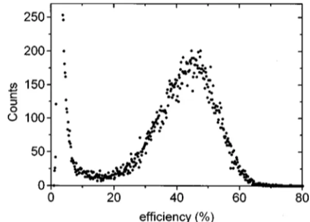
Particle detectors were then realized by thermally evapo-rating a circular Au contact about 7 mm2in size and 100 nm thick as the top electrode, while Ag paste was used as the silicon backing contact. The detector response to 5.5 MeV␣ particles was studied using a 241Am source. The irradiation was carried out through a pinhole, in the normal direction to the sample surface. The detector output has been connected, through a charge preamplifier and a shaping amplifier with a 2 s shaping time, to a multichannel analyzer. A typical collection spectrum of our samples is reported in Fig. 1. In our experience, contact configurations others than the ones we used 共e.g., Ti/Au or Cr/Au top contacts, free standing films with Au contacts on both sides兲 make no difference in these measurements.
We choose␣particles rather than, e.g.,90Sr particles as the radiation probe because minimum ionizing particles, like 90Sr  particles, would not deposit sufficient energy in our thinner films to allow a reasonably accurate measure-ment of efficiency and CCD. In addition, 241Am␣ particles create charges only within a depth of 15m from the growth surface of the films, so that the effects of in-grain defects 共homogeneously distributed兲 and grain boundaries 共concen-trated at the diamond–substrate interface兲3 are better sepa-rated. A drawback of the high ionization produced by␣ par-ticles is the occurrence of polarization effects, causing a systematic decrease of the detector response during the
mea-surement. In our case this effect was minimized reducing the fluence of ␣ particles to a few counts per second. Spectra collected immediately after applying the electric field and after 5 min 共our measurement time兲 differed by less than 10%. In addition, samples turn back with time 共or by apply-ing reverse bias兲 to the ‘‘virgin’’ state, in the sense that their spectra revert to the ones initially measured on the same sample. The reproducibility of efficiency and CCD values extracted from spectra taken in this virgin state for a given sample is within a few percent.
All charge collection spectra have been measured at room temperature under positive bias 共i.e., the growth sur-face electrode was positively biased, the back contact being grounded兲. Each measurement took 5 min. Samples were measured both in the as-grown state and after preirradiation with90Srparticles for the time共typically about 60 h兲 nec-essary to drive the film in a fully pumped state, as deter-mined by the charge collection spectrum, which was unaf-fected by further irradiation. The total radiation dose absorbed by the samples is about 3 krad. Charge collection spectra in the pumped state were measured within 24 h from completion of the pumping process. Measurements repeated on the same sample after several days proved that the pumped state remains stable over at least a week provided, as in our case, that the sample is not exposed to strong light sources, normal ambient light resulting in no measurable depumping on this time scale.
In all cases the whole film has been utilized to build the detector, i.e., without removing, as is normally done in order to increase the detector performance 共see e.g., Ref. 1兲, the low quality layer close to the substrate interface.
Set 1 was realized to study whether the higher growth rates obtainable using more carbon-rich plasma are compat-ible with the production of high efficiency detectors. A de-crease of the detectors’ performance with increasing carbon concentration was observed for several gas mixtures,2,8 but only detectors in the unpumped state were considered in these studies. It is clearly of great importance to know whether the pumping process can overcome this problem, since the time needed to grow diamond samples thick enough to be used as nuclear detectors is extremely long using the CVD technique.
FIG. 1. Typical␣-particle collection spectrum of our films in the pumped state.
TABLE I. Sample thickness and CH4concentration in the growth gas mix-ture for the CVD diamond investigated in the present work.
Sample
Set No. 1 Set No. 2
A B C D E F B G H
CH4共%兲 0.6 1.0 1.4 1.8 2.2 1.0 1.0 1.0 1.0
Set 2 was instead prepared to better clarify the role of grain boundaries and in-grain defects in the detection process of CVD diamond before and after the pumping process, also in view of the simple model recently proposed3 to explain the effects of pumping. The film thickness is varied from about 20 m 共i.e., just above the penetration depth of 5.5 MeV␣particles兲 to about 160m.
RESULTS AND DISCUSSION
The main parameters assessing the performance of par-ticle detectors are the CCD and the efficiency, defined as follows for a standard experimental setup in which a parallel plate detector is used. An electron–hole pair created by an ionizing particle in a parallel plate detector of thickness共i.e., electrode spacing兲 L, induces9,10 in the external circuit a charge qc⫽ex/L, x being the total distance the electron and
hole move apart under the action of the applied electric field. The CCD is the average distance electrons and holes would drift apart, and is given by
␦⫽共e⫹h兲E, 共1兲
where e,h are the electron and hole mobilities, respec-tively, is the mobility weighted lifetime of electrons and holes, and E is the applied electric field. The efficiency is the ratio of the collected charge Qcto the total charge Q0 gen-erated by the ionizing particle
⫽Qc/Q0. 共2兲
The link between and␦ can be deduced from the Hecht theory11
⫽␦L
冋
1⫺ ␦ 4G共1⫺e⫺共2G/␦兲兲共1⫹e2共G⫺L兲/␦兲
册
, 共3兲 G being the penetration depth in L of the particles to be detected 关in Eq. 共3兲 we assumed e⫽h兴. The lifetime ,and therefore␦and, are limited by the presence of trapping defects 共impurities and/or grain boundaries兲, so that the col-lection efficiency is strongly correlated with crystal quality. Strictly speaking, Eq. 共3兲 could not be used for CVD dia-mond detectors since it is derived for a uniform material, however it provides a useful and widely used estimate of the CCD.
In Fig. 2 the behavior of the average efficiency of the detectors of set 1 is shown as a function of the methane content in the plasma, both in the normal and in the primed state. The applied voltage is 68 V, so that the electric field is about 15 kV/cm共see below兲. A negative correlation can be seen in both cases, showing the progressive reduction of the quality of the films as the carbon content in the growth mix-ture, and therefore the growth rate, is increased. This con-firms the results of Ref. 2, which anyway did not include the primed state behavior and where no indication of the thick-ness of the various films was given. It has been demonstrated12 that the decrease in the detectors’ efficiency is accompanied by a moderate widening of the Raman peak and by a relatively more marked increase of the photolumi-nescence background peaked at about 3000 cm⫺1, and is therefore strictly connected to sample quality.
Another important disadvantage in using high methane concentrations is the reduced ability of the detectors to with-stand high applied electric fields, especially in the pumped state. In particular, efficiency measurements of films grown at high methane concentrations共⬎1.4%兲 in the pumped state were not possible because of the low electric breakdown threshold observed in these films.
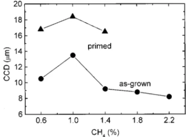
In addition, the CCD versus CH4 plot in Fig. 3 shows that the CCD value slightly decreases with methane concen-tration. We point out that all detectors show well defined peaks in the charge collection spectra, both in the as-grown and in the pumped state.
Some considerations are necessary to correctly analyze the results shown in Figs. 2 and 3. In principle, all samples belonging to set 1 were supposed to have the same thickness 共40m兲, with only the CH4content changed. The increase in growth rate with CH4concentration, however, lead to thick-ness increasing from 30 m 共sample A兲 to 53m共sample E兲, as reported in Table I. This could partly obscure the conclusions drawn upon these results. However, although the thicknesses of films belonging to set 1 are not all equal to the intended 40 m value, it turns out that the efficiency and CCD values would not change significantly if all films were 40 m thick, so that the previous conclusions are substan-FIG. 2. Average efficiency vs methane concentration in the growth gas mixture for the detectors of set 1, in both the as-grown共circles兲 and pumped 共triangles兲 states. Lines are guides to the eye.
FIG. 3. Average charge collection distance vs methane concentration in the growth gas mixture for the detectors of set 1, in both the as-grown共circles兲 and pumped共triangles兲 states.
tially correct. The reason for this is that as the film thickness varies from 30 m共sample A兲 to 53 m 共sample E兲, two effects of opposite sign must be considered, namely共a兲 being the applied voltage fixed to 68 V, the thicker films 共higher CH4 concentration兲 were measured under a lower electric field E, leading toand CCD values decreased with respect to those of a 40 m film;共b兲 their higher thickness leads to higher efficiency values共see Fig. 4兲 and therefore to, and CCD values increased with respect to those of a 40m film 共the opposite holds for thinner films兲. These corrections can be calculated from the versus E共see e.g., Ref. 3, Fig. 2兲 and versus thickness共see Fig. 4兲 curves, and it turns out that in this thickness and electric field region, they are both rather small共less than 10%–15%兲 and almost exactly cancel each other. Values reported in Figs. 2 and 3 therefore repre-sent very well the behavior of films of strictly equal thick-ness共40m兲 whose quality is changed by varying the meth-ane concentration in the growth mixture.
From Figs. 2 and 3 we see that for set 1 there is only a moderate difference between the CCD and efficiency values in the unprimed and primed state. This is due to the rela-tively low thickness of these detectors, leading to a grain size close to the mean free path of carriers due to in-grain defects. In Ref. 3 the defects leading to a limitation of the CCD were divided into in-grain defects and grain boundaries, the former being homogeneously distributed and saturated by the pumping process, the latter strongly concentrated toward the substrate side because of the columnar nature of CVD dia-mond growth, and unaffected by preirradiation. It was shown that under these assumptions it was possible to reproduce by Monte Carlo simulations the␣-particle collection spectra of a high efficiency CVD diamond detector. It is then clear that when the grain size is comparable or smaller than the mean free path due to in-grain defects, only a moderate effect is to be expected from the pumping process, since grain bound-aries are the main obstacle to high CCD values even in the as-grown state. As the film thickness and grain size increase, however, the saturation of in-grain defects should lead to substantial improvements in the efficiency and CCD of the detectors according to this model. This was the reason which prompted us to grow the samples of set 2, in which the
growth conditions were kept constant, with only the growth time being changed in order to obtain films only differing in their thickness.
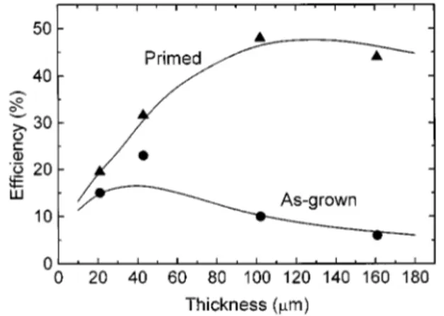
Figure 4 shows that indeed the efficiency versus thick-ness behavior of our detectors confirms the above reported expectations, a very high efficiency increase taking place when the thickness exceeds 40–50 m. The curves relative to the as-grown and pumped states show a different behav-ior. In the former case the efficiency initially increases with thickness and then, for d⬎40m decreases roughly follow-ing a 1/d law, while in the latter case the efficiency steadily increases up to a thickness of 100 m, and then slightly decreases. The applied electric field is 15 kV/cm for all films.
The results of Fig. 4 are better explained after looking at Fig. 5, where the dependence of the CCD on the detectors’ thickness is plotted both in the normal and the pumped state. In the normal state the CCD value is very small for the 21 m thick film, while for the other films (d⬎40m) it is substantially independent from thickness, with a value close to 12m. This behavior is expected in the framework of the assumption made in Ref. 3 that defects limiting the collec-tion length can be divided into in-grain defects and grain boundaries, which are distributed differently because of the columnar growth of CVD diamond. For very low thickness values the microgranularity of the substrate interface layer prevents significant drift lengths of the carriers, so that the CCD is very low. As the film thickness increases, so do grain dimensions, and the free path of carriers sharply increases until eventually grain dimensions are so large that grain boundaries play a minor role. In this case the CCD is limited by the substantially homogeneous distribution of in-grain de-fects and the curve of Fig. 5 flattens out. Such a view is confirmed by the behavior after pumping, which in Ref. 3 is proposed to saturate in-grain defects only. For films of low thickness, grain boundaries play a major role in limiting the drift lengths and pumping has therefore a very limited effect. However, eventually the average grain dimension becomes larger than about 12m, which is the mean free path due to in-grain defects 共Fig. 4兲, and hence the saturation of such defects becomes important. As a consequence the pumped FIG. 4. Average efficiency vs film thickness for the detectors of set 2, in
both the as-grown共circles兲 and pumped 共triangles兲 states. Lines are simula-tions based on the model described.
FIG. 5. Average charge collection distance vs film thickness for the detec-tors of set 2, in both the as-grown共circles兲 and pumped 共triangles兲 states. Lines are simulations based on the model described.
curve instead of flattening out continues to increase, reflect-ing the continuously increasreflect-ing grain dimensions. Also this curve is clearly expected to eventually saturate if the pump-ing process does not completely neutralize in grain defects, but no clear signal of such a saturation is observed from our data up to a film thickness of 160 m, so that margins for even higher CCD values can be foreseen. We notice that the normal state and pumped curve depart when the film thick-ness is about 40 m, and since grain dimensions are typi-cally 1/3–1/4 of the film thickness this agrees well with the 12m CCD value.
For our thicker film 共161 m兲 the CCD value corre-sponding to the average 44% efficiency is 145m, while the same film shows a maximum efficiency close to 70%, which corresponds to a CCD of 370 m. The record high CCD value reported so far1 is 280m, measured on 1 mm thick film produced by De Beers. This result cannot be directly compared with our values, since it was obtained with par-ticles, which penetrate the whole detector and therefore also sample the lower quality region close to the substrate side. It is difficult to determine the correction factor, but it can be estimated that in sufficiently thick samples, the CCD esti-mated using ␣particles is twice that measured using par-ticles. However, this disadvantage is at least partly compen-sated in Ref. 1 by the removal of about half of the detector thickness from the lower quality substrate layer and by the extremely high thickness of the detector, almost ten times higher than our thicker film. Also, our CCD value is higher than film thickness, and therefore an increase in thickness is likely to lead to higher CCDs.
Coming back to Fig. 4, its interpretation is now straight-forward. The initial efficiency increase in the normal state is due to grain dimension reaching values comparable to the carriers mean free path due to in-grain defects 共about 12 m兲, and the following decrease takes place when grain di-mensions exceed this length so that in-grain defects limit the CCD. In this case the CCD remains constant anddecreases with thickness according to Eq.共3兲. On the other hand, in the pumped state the efficiency almost monotonically increases because the increase in CCD compensates thickness varia-tion in Eq. 共3兲. Eventually, of course, the efficiency is ex-pected to reach a limiting value. This limiting value should in principle increase by removing the low quality substrate layer of the detectors.
Since the general trends shown in Figs. 4 and 5 are well in agreement with our model, we tried to quantitatively com-pare them to the results of a Monte Carlo simulation based on the model. The calculated versus thickness and CCD versus thickness curves are shown as full lines in Figs. 4 and 5, respectively. It appears that the simulated curves match the experimental data closely enough, with the only excep-tion being the efficiency value of the 43 m thick film, which is underestimated by our simulation. Nevertheless, considering that the model is clearly a simplified one, this agreement seems quite satisfactory. The general trends ob-served forand the CCD are clearly related to the different behavior and distribution of in-grain defects and grain boundaries. Within this general concept, a more detailed analysis of features like, e.g., the number and type of
in-grain defects, the in-grain boundaries distribution and the dif-ferent behavior of electrons and holes would naturally im-prove quantitative agreement with the data. However, for such an analysis to be meaningful, probably greater experi-mental evidence on CVD diamond physics would be re-quired than is presently available. To calculate the simulated curves the distribution of the grain boundaries共unaffected by pumping兲 and the mean drift distance of carriers before trap-ping due to in-grain defects in both the as-grown (l0) and pumped (lP) states are required. Assuming an exponential
density3of grain boundaries D(x)⫽A exp(⫺x/b) to describe the columnar growth, with x the distance from the film– substrate interface, only four parameters are necessary to ob-tain all the curves in Figs. 4 and 5. The values we adopted for these parameters are A⫽5.3m⫺1, b⫽11m, l0 ⫽10.3m, and lP⫽175m. The reasonable values of these
parameters constitute more evidence in favor of the proposed model. In particular, from these numbers it turns out that after pumping the concentration of active in-grain traps de-creases by more than 1 order of magnitude, confirming the effectiveness of preirradiation in improving CVD diamond particle detectors quality.
CONCLUSIONS
We have presented a systematic study of the perfor-mances of particle detectors built from high quality CVD diamond films. The influence of both the growth conditions 共leading to films of different quality兲 and of the film thick-ness has been carefully investigated. The increase in methane content in the growth gas mixture leads to a decrease in the detector’s efficiency and in the electric field that can be ap-plied to the films, while a higher thickness leads to higher efficiency and CCD values. Our best detector共about 160m thick兲 has an average 44% efficiency, with a maximum value close to 70%, corresponding to CCD values of 145 and 370 m, respectively.
Particular attention has been given to the pumping effect and its influence on the detectors’ performance. The results are analyzed in the framework of a recently proposed model3 taking into account the columnar growth of CVD diamond, in which in-grain defects and grain boundaries are assumed to behave differently after the pumping process. Experimen-tal data fully support our model, which allows us to quanti-tatively reproduce the observed results, thus giving grounds to the proposed microscopic interpretation of the pumping process in polycrystalline CVD diamond. As a result, the successful interpretation of film’s performance gives a firm basis to the expectation of even higher CCD values to be obtained by scaling up film thickness.
1W. Adam et al., 5th International Symposium on Diamond Materials, Paris, 1997, edited by J. L. Davidson et al., Proceedings of the Electro-chemical Society, Vol. 97-32共Pennington, NJ, 1998兲, p. 491.
2T. Behnke, A. Oh, A. Wagner, W. Zeuner, A. Bluhm, C-P. Klages, M. Paul, and L. Schaefer, Diamond Relat. Mater. 7, 1553共1998兲.
3M. Marinelli, E. Milani, A. Paoletti, A. Tucciarone, G. Verona Rinati, M. Angelone, and M. Pillon, Appl. Phys. Lett. 75, 3216共1999兲.
4G. Balestrino, M. Marinelli, E. Milani, A. Paoletti, I. Pinter, and A. Tebano, Appl. Phys. Lett. 62, 879共1993兲.
5M. Marinelli, E. Milani, M. Montuori, A. Paoletti, P. Paroli, and J. Tho-mas, Appl. Phys. Lett. 65, 2839共1994兲.
6M. Marinelli, E. Milani, A. Paoletti, A. Tucciarone, G. Verona Rinati, G. Messina, M. Angelone, and M. Pillon, Proceedings of Applied Diamond Conference/Frontier Carbon Technology Joint Conference, Tsukuba, Ja-pan, August 31–September 3, 1999, p. 154.
7
A. A. Morrish and P. E. Pehrsson, Appl. Phys. Lett. 59, 417共1991兲. 8M. Marinelli, E. Milani, A. Paoletti, A. Tucciarone, G. Verona Rinati, N.
Randazzo, R. Potenza, M. Pillon, and M. Angelone, Diamond Relat. Mater. 7, 519共1998兲.
9W. Shockley, J. Appl. Phys. 9, 635共1938兲. 10S. Ramo, Proc. IRE 27, 584共1939兲. 11K. Hecht, Z. Phys. 77, 235共1932兲. 12
G. Faggio, M. Marinelli, G. Messina, E. Milani, A. Paoletti, S. Santan-gelo, A. Tucciarone, and G. Verona Rinati, Diamond Relat. Mater. 8, 640