Superconducting proximity effect and interface transparency in Nb/ PdNi bilayers
C. Cirillo, S. L. Prischepa,*M. Salvato,†and C. Attanasio‡Dipartimento di Fisica “E. R. Caianiello” and Laboratorio Regionale SuperMat INFM-Salerno, Università degli Studi di Salerno, Baronissi (Sa) I-84081, Italy
M. Hesselberth and J. Aarts
Kamerlingh Onnes Laboratory, Leiden University, P.O. Box 9504, 2300 RA Leiden, The Netherlands 共Received 11 April 2005; revised manuscript received 5 July 2005; published 14 October 2005兲 The proximity effect between a superconductor共S兲 and a weak ferromagnet 共F兲 in sputtered Nb/Pd0.86Ni0.14 bilayers has been studied. The dependence of the critical temperature on the S- and F-layer thicknesses can be interpreted in the framework of recent theoretical models and yields reasonable numbers for the exchange energy of the ferromagnet and the interface transparency of the S/F barrier.
DOI:10.1103/PhysRevB.72.144511 PACS number共s兲: 74.45.⫹c, 74.78.Fk
I. INTRODUCTION
The investigation of the interplay of superconductivity and ferromagnetism in S/F hybrids is a very active area of research. The renewed interest in proximity effects in these systems is due both to the development of technology, which makes possible to fabricate heterostructures consisting of very thin layers, and to the intriguing physics behind them. Such S/F hybrid structures are important from a scientific point of view since they allow the investigation of the inter-play between two antagonistic phenomena, superconductiv-ity and ferromagnetism,1,2 as well as the study of applica-tions such as F/S/F spin valves3,4and S/F/S-junctions.5,6
Here we will focus our attention on S/F bilayers. For these structures a nonmonotonic behavior of the critical tem-perature as a function of the thickness of the ferromagnetic layer has been found theoretically7–11 as well as experi-mentally.12,13 The presence of the exchange field Eex in F causes an energy shift between the quasiparticles of the pair entering the ferromagnet and this results in the creation of Cooper pairs with nonzero momentum.8This implies that the superconducting order parameter does not simply decay in the ferromagnetic metal, as it happens in normal metals, but also oscillates over a length scale given byF, the coherence length in F. This length can be estimated from the dirty limit expression:6
FDirty=
冑
បDFEex
, 共1兲
where DFis the diffusion coefficient of the F-metal. Quali-tatively, the nonmonotonic behavior of the transition tem-perature can be seen as a consequence of the interference of quasiparticles共electrons and holes兲 that experience Andreev reflections at the S/F interface and normal reflections at the vacuum interface of the F layer. This interference can be constructive or destructive depending on the thickness dFof the F layer8–10 and can lead to oscillations of the supercon-ducting transition temperature Tcas a function of dF. Experi-mentally, such oscillations in F/S/F trilayers have been ob-served in systems involving, for instance, Fe or Co as ferromagnet,14–16 and in the Fe/ V system even re-entrant
superconductivity.17 However, in these systems with strong ferromagnets and exchange energies typically of the order of 1 eV,FDirtyis of the order of 0.1–1 nm, which is very difficult to control experimentally. Furthermore, in this thickness range different complications can be present, such as inter-diffusion or alloying effects, resulting in a magnetically dead layer,12,14 or interfacial roughness,18 all of which strongly influence the interface transparency,T. This crucial param-eter dparam-etermines the strength of the proximity effect and is not directly measurable, but it is clear that the non-perfect trans-parency of the interfaces greatly reduces the amplitude of the order parameter oscillation,9,10which also explains why ex-periments on the same material combinations may yield dif-ferent results.
For these reasons, systems where the F layer consists of a magnetic alloy whose exchange energy can be controlled by varying the amount of magnetic component, are of great in-terest. This is the case for Pd1−xNix共0⬍x⬍0.2兲, where Eex can be varied in the meV range by changing the Ni concen-tration in the highly paramagnetic metallic matrix of Pd. In this system,FDirtyis of the the order of 3–6 nm, a thickness accessible to standard deposition techniques. Another advan-tage of the Nb/ Pd1−xNix is that interdiffusion between the
two layers will be limited by the bcc/fcc interface. It is also of interest to compare Pd1−xNix to other weak ferromagnets
such as Cu1−xNix, where weak oscillations in Tc were
observed.19,20An extra reason to compare the two systems is that the Nb/ Pd system possibly yields higher values of the interface transparency21,22than the ones based on Nb/ Cu.23
In the present paper we present measurements of the su-perconducting critical temperatures of Nb/ Pd0.86Ni0.14 bilay-ers and we extract parametbilay-ers which describe this behavior. A brief description of the sample preparation and character-ization and the results of the transport measurements are pre-sented in Secs. II and III, respectively. In Sec. IV the experi-mental results are fitted in the framework of the theoretical model developed by Fominov10to derive microscopic prox-imity effect parameters, in particular the exchange energy of the ferromagnet and the transparency T of the Nb/ Pd0.86Ni0.14barrier. These values will be compared to the ones obtained for other S/F systems as well as for the corre-spondent S/N system, Nb/ Pd, in Sec. V.
II. SAMPLE PREPARATION AND CHARACTERIZATION Bilayers of Sub/ Pd0.86Ni0.14/ Nb 共where Sub denotes the substrate兲 were grown in a dual source dc triode magnetron sputtering system on Si共100兲 substrates. A movable substrate holder allows to fabricate 8 different samples in a single deposition run. The deposition conditions were similar to those of the Nb/ Pd multilayers described earlier.21,24Three different sets of bilayers were prepared. One set, with the Nb thickness dNbfixed at 35 nm, was deposited to study Tcas a
function of the ferromagnetic layer thickness, dPdNi. Two sets, consisting of a Pd0.86Ni0.14layer with constant thickness 共dPdNi= 48.4 nm兲 and a Nb layer with variable thickness 共dNb= 10– 150 nm兲 were used to determine Tc共dNb兲 behavior. Moreover, one set of single Nb films with different thick-nesses was deposited, in order to study the intrinsic suppres-sion of the critical temperature with the Nb thickness. Single Pd0.86Ni0.14 films were also grown to study the magnetic properties of the alloy.
In the fabrication of artificially layered structures for the study of proximity effect, attention must be paid to interface properties. In particular, in order to have transparent barriers the existence of flat layers and of interfaces with small roughness is essential. For this reason the interface quality was studied by x-ray reflectivity measurements, using a Phil-ips X-Pert MRD high resolution diffractometer. The x-ray reflectivity analysis was performed on bilayers deliberately fabricated with appropriate thicknesses under the same con-ditions as for the samples used in superconductivity mea-surements. The reflectivity profile of a Sub/ Nb/ Pd0.86Ni0.14 bilayer with dNb= 18.0 nm and dPdNi= 23.7 nm is shown in Fig. 1 together with the simulation curve obtained using the Parrat and Nevot–Croce formalism.25,26The fit reveals that the bottom Si/ Nb interface has a roughness value of 1.2 nm, while the top Nb/ Pd0.86Ni0.14 interface has a smaller rough-ness of about 0.7 nm. The film thickrough-nesses obtained from the simulation were used for the final calibration of dNb and
dPdNi.
The onset of ferromagnetism in Pd1−xNixalloys is around
x = 0.023.27 In order to have magnetic homogeneity a Pd1−xNix target with x = 0.10 was used. This stoichiometry
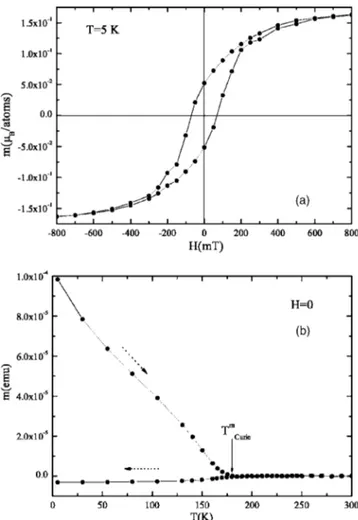
was not conserved in the samples as revealed by the Ruther-ford backscattering analysis, which gives a Ni concentration of x = 0.14. The hysteresis loop of a Pd0.86Ni0.14 single film, 48.4 nm thick, is presented in Fig. 2共a兲. The measurements were performed by a SQUID magnetometer at a temperature of 5 K with the surface of the sample parallel to the magnetic field. At this temperature the value of the saturation magnetic moment is msat= 0.17B/ atom, while the coercive field is about 70 mT. For the same sample, the temperature depen-dence of the magnetic moment m was measured, in order to derive the value of the Curie temperature, TCuriem . The sample was magnetized to saturation at 5 K, the field was then re-moved and m共T兲 was measured up to 300 K and down again to 5 K. TCuriem was defined as the point where irreversibility appears when cooling down the sample, and was estimated to be TCuriem = 185 K. Also the resistance R of the sample was measured between 300 K and 4 K, as shown in Fig. 3. A clear shoulder is observed around 210 K. The connection to the magnetic ordering becomes more clear from the behavior of the derivative of R with respect to T, dR共T兲/dT, plotted in the insert. Between 300 K and 220 K, dR共T兲/dT decreases, FIG. 1. Experimental共solid line兲 and calculated 共dashed line兲
low-angle reflectivity profile for a Nb/ Pd0.86Ni0.14bilayer. The
nu-merical simulation is arbitrarily shifted downward for sake of clearness.
FIG. 2. 共a兲 Magnetization loop for a single Pd0.86Ni0.14film at T = 5 K.共b兲 Magnetic moment as a function of the temperature for the same film, after saturation at T = 5 K. The dotted arrows indicate the measurement sequence.
followed by a steep rise between 220 K and 190 K, after which dR共T兲/dT flattens. The behavior can be compared to that of magnetic ordering in other metallic systems,28where the minimum in dR共T兲/dT is due to short-range fluctuations just above TCurie, while TCurieitself is found at the maximum below the steep rise. If we simply define TCurieR as the tem-perature where the rise flattens, we find TCurieR ⬇200 K, in reasonable agreement with TCuriem .
III. SUPERCONDUCTING PROPERTIES
The superconducting transition temperatures Tcwere
re-sistively measured using a standard dc four-probe technique.
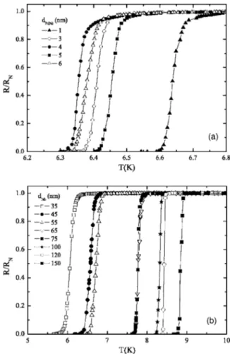
Tcwas defined as the midpoint of the transition curve. In Fig.
4, examples are presented of such transitions for some samples from both the series with variable PdNi thickness
dPdNiand with variable Nb thickness dNb, respectively. In the first case, the widths of the transitions never exceeded 0.1 K, while for the series with variable Nb thickness they were typically less than 0.2 K. The measured values of the Nb resistivity of samples 200 nm and 35 nm thick, were 6⍀ cm and 17⍀ cm, respectively. The electrical resis-tivity of a 30 nm PdNi film wasPdNi= 24⍀ cm, while the resistivity of thinner PdNi films between 1–9 nm was around 50⍀ cm.
In Fig. 5 the dependence of the superconducting transition temperature on the thickness of the PdNi layer, with dNb fixed at 35 nm, is shown. The bulk value TcS= 7 K is the
transition temperature of a single Nb film with dNb= 35 nm. Increasing dF, Tc exhibits a rapid drop, until a saturation
value is obtained.
The dependence of the critical temperatures Tc on the
thickness of the Nb layer dNb, with dPdNifixed at 48.4 nm, is shown in Fig. 6. The transition temperature of the sample with dNb= 15 nm is not reported since it was below 1.8 K, the lowest temperature reachable with our experimental setup. In
Fig. 6, the critical temperatures Tc共dNb兲 are compared to those of single Nb films共open symbols兲, indicating that the suppression of the superconducting transition temperature of Nb/ PdNi bilayer is due to the proximity effect rather than to the intrinsic thickness dependence of the single Nb. The last is described by the phenomenological relation:
Tc共dNb兲 = Tc0共1 − d0/dNb兲 共2兲 with Tc0= 9.2 K and d0 the minimum thickness of the Nb film with Tcdifferent from zero. The dotted curve in Fig. 6 is
obtained for d0= 8 nm.
IV. ANALYSIS OF THE DATA
This section deals with the interpretation of the experi-mental results, by fitting them in the framework of a theoret-ical model which explicitly takes into account the exchange energy of the ferromagnet Eexand the interface transparency
T. The first well known theory for S/F proximity effect was
the one by Radovic.29 However, even though it well de-scribes the behavior of critical temperatures and critical fields, this theory assumes a perfect interface, a condition FIG. 3. Electrical resistance as a function of temperature for a
PdNi single film, 48.4 nm thick. Inset: magnification of the main panel data共open symbols兲 compared with its first derivative 共closed symbols兲. The arrow indicates the value of the Curie temperature derived from the m共T兲 measurement.
FIG. 4. Resistive transitions R共T兲 normalized respect to RN
= R共10 K兲 for some of the measured samples from the different sets: 共a兲 series with constant Nb thickness dNb= 35 nm and variable PdNi
thickness, dPdNi= 1 – 3 – 4 – 5 – 6 nm; 共b兲 series with constant PdNi thickness dPdNi= 48.4 nm and variable Nb thickness, dNb
which is never fulfilled in real systems. T is a parameter which describes the resistance experienced by electrons crossing the barriers between two metals. Interface imperfec-tions, mismatches between Fermi velocities and band struc-ture of the two metals all act as a potential barrier at the interface, that screens the proximity effect. These are the
possible causes of the reduction ofT in S/N systems. At the S/F barrier the transparency can undergo an additional de-crease, due to the polarization of the conduction electrons in the ferromagnet and to the spin dependent impurity scattering.30,31
The theoretical model developed by Fominov,10 consid-ered in this paper, takes a weak exchange field and the finite transparency of the interfaces explicitly into account. More-over, this theory was already applied in the case of another weak ferromagnetic alloy, namely Nb/ Cu0.43Ni0.57, while the analogous model developed by Tagirov,9formulated in terms of a clean regime 共long mean free path, lF⬎F兲 is more
suited for strong ferromagnets. The starting point of Fomi-nov’s model are the linearized Usadel equation,32 with the boundary conditions derived by Kupriyanov and Lukichev33 for the pairing function at the outer surfaces of the bilayers:
dFS共dS兲
dx =
dFF共− dF兲
dx = 0 共3兲
as well as at the S/F boundary:
S dFS共0兲 dx =␥F *dFF共0兲 dx , ␥= SS FF *, 共4兲 F *␥ b dFF共0兲 dx = FS共0兲 − FF共0兲, ␥b= RBA FF* , 共5兲 where S=
冑
បDS 2kBTcS , 共6兲 F*=冑
បDF 2kBTcS . 共7兲HereS,Fand DS,F are the low temperature resistivities and the diffusion coefficients of S and F, respectively, while RBis
the normal-state boundary resistivity andA is its area. Note thatF
*
does not depend on Eex, and is therefore not the same asFDirty. The parameter␥is a measure of the strength of the
proximity effect between the S and F metals while ␥b
de-scribes the effect of the interface transparency T. In this modelT is defined as:
␥b= 2 3 lF F* 1 −T T . 共8兲
T is zero for the completely reflecting interface 共large
resis-tance of the barrier RB兲 and it is equal to one for a completely
transparent one. It is useful to compare this definition to the
Tmpresent in Tagirov’s model9and reported in a number of
experiments.13,15,17,44The two definitions are linked through the expression:
Tm=
T
1 −T , 共9兲
where this time Tmcan vary between zero共negligible
trans-parency兲 and infinity 共perfect interface兲. FIG. 5. The critical temperature Tcversus PdNi thickness dPdNi
in Nb/ Pd0.86Ni0.14 bilayers with constant Nb thickness dNb
= 35 nm. Different lines共dotted, solid, and dot-dashed兲 are the re-sults of the theoretical fit in the single mode approxi-mation for different values of␥b. The insert shows a comparison
between the single mode共䊊兲 and the multimode 共⫻兲 calculations for Eex= 150 K. The drawn line is a single mode calculation for
Eex= 170 K.
FIG. 6. The critical temperature Tcversus Nb thickness dNbin Nb/ Pd0.86Ni0.14 bilayers with constant PdNi thickness dPdNi
= 48.4 nm. Different closed symbols refer to samples sets obtained in different deposition runs. Open symbols refers to single Nb films. The dotted line describes the phenomenological Tcthickness depen-dence of Nb single films. The solid line is the result of the theoret-ical calculations in the single mode approximation. The fitting pa-rameters are given in the text. Inset: Tc共dNb兲 curves for Nb/Pd
共open symbols兲 and Nb/PdNi 共closed symbols兲. The solid and the dot-dashed lines indicate the results of the theoretical calculation reported above and in Ref. 21, respectively.
It is important to note that the boundary condition 共5兲 determines a jump of the pairing function at the interface, in contrast with Radovic’s picture, in which, due to the perfect boundary, the pairing function varies continuously.
The above problem can be solved analytically only in limiting cases. One of them, often used, is the single-mode approximation. In this case the critical temperature of the bilayer is determined by the equations:
ln
冉
TcS Tc冊
=⌿冉
1 2+ ⍀n 2 2 TcS Tc冊
−⌿冉
1 2冊
, 共10兲 ⍀ntan冉
⍀n dS S冊
= W共n兲, 共11兲 with W共n兲 =␥ AS共␥b+ ReBF兲 +␥ AS兩␥b+ BF兩2+␥共␥b+ ReBF兲 , 共12兲 BF=关kFF*tanh共kFdF兲兴−1, kF= 1 F *冑
兩n兩 + iEexsgnn kBTcS , 共13兲 AS= kSStanh共kSdS兲, kS= 1 S冑
n kBTcS . 共14兲where n=Tc共2n+1兲 with n=0, ±1, ±2,… are the
Matsubara frequencies, ⌿共x兲 is the digamma function and
TcS is the critical temperature of the single S layer.
In this approximation only the real root⍀0of Eq.共10兲 is taken into account, while the other imaginary roots are ne-glected. The exact multi-mode solution is obtained by taking also the imaginary roots of ⍀ into account. As shown by Fominov10in the general case the results of the two calcula-tions can be different and the single-mode method is appli-cable only if the experimental parameters are such that W can be consideredn independent. In particular in the case
when Eex/TcS⬎1 and dF⬃F the method is valid if
冑
Eex/共Tcs兲Ⰷ1/␥b. We shall use the single-modeapproxi-mation and compare it to the full共multi-mode兲 calculation.34 A large number of microscopic parameters appears in Eqs. 共10兲–共14兲. However, part of them can be derived indepen-dently. The electrical resistivities were determined experi-mentally. The Nb coherence length, S, can be determined
through the expression 共6兲, where the diffusion coefficient
DSis related to the low temperature resistivitySthrough the
electronic mean free path lS by Ref. 35
DS= vSlS 3 共15兲 in which lS= 1 vS␥SS
冉
kB e冊
2 , 共16兲where␥S⬅␥Nb⬇7⫻10−4J / K2cm3is the Nb electronic spe-cific heat coefficient36 and v
S⬅vNb= 2.73⫻107cm/ s is the
Nb Fermi velocity.37 In this way the value obtained for the mean free path and for the coherence length of the single Nb film of the series with variable PdNi thickness, 35 nm thick, with TcS= 7 K and Nb= 17⍀ cm are lNb⬇2.3 nm and
Nb⬇6 nm, respectively. The coherence length F* is
deter-mined according to Eq.共7兲. As we found that the resistance of the F layers depends on thickness below 30 nm, we assume that the PdNi mean free path is thickness-limited and use an average value of lF⬇4 nm; together with the Pd
Fermi velocityvF⬅vPd= 2.00⫻107cm/ s共Ref. 38兲 this leads to a value ofF
*
= 6.8 nm. In this way Eexand␥bare used as
the only free parameters in the theory. The fitting procedure consisted in determining Eexvalue where Tcstarts to saturate
as function of dPdNi, while ␥b was used to control of the
vertical position of the curve.
The solid line in Fig. 5 is obtained as the result of the calculations for Eex= 150 K and␥b= 0.55, with the fixed
pa-rameters dNb= 35 nm, TcS= 7 K, Nb= 6 nm, PdNi
* = 6.8 nm,
PdNi= 50⍀ cm, andNb= 17⍀ cm. The fits are quite in-sensitive to the value of Eex, as can be seen in the insert, where a curve with Eex= 170 K is displayed for comparison. A reasonable error bar is Eex= 150 K ± 20 K. Theoretical fits for different values of␥b are also given, and show that the
fits are quite sensitive to the value of␥b.
The formation of a possible Nb oxide layer at the top of the bilayers was also considered. An oxide layer 1.5 nm thick, and the consequent reduction of the effective Nb layer, would affect the theoretical fit, leading to a value of ␥b
= 0.65. This effect, together with the dispersion of the experi-mental points, allows to estimate an error bar of ␥b
= 0.60± 0.15.
From the data in Fig. 5, a good estimate can be obtained forF
Dirty
. As can be inferred from the calculations presented in Ref. 10, this parameter is phenomenologically related to the position of the minimum in Tc共dF兲 according to dmin = 0.7FDirty/ 2. With dmin⬇3.8 nm, we findFDirty⬇3.4 nm, in very good agreement with the value of 3.7 nm which can be obtained from Eq. 共1兲. The insert of Fig. 5 also shows a comparison of the single mode and the full multimode calculation. This is reasonable in view of the fact that the limit of applicability of the single mode calculation
冑
Eex/共Tcs兲 共⬇3兲Ⰷ1/␥b共⬇2兲 is fulfilled.With the same set of equations the behavior of Tc共dNb兲 was also reproduced. In the theoretical calculations the in-trinsic critical temperature dependence of the single Nb films was taken into account through relation共2兲. The solid line in Fig. 6 represents the model calculation obtained using the values for Eexand␥bobtained from the Tc共dPdNi兲 fit, and the fixed parameter values TcS= 7 K, Nb= 6 nm, PdNi
*
= 6.8 nm,
PdNi= 24⍀ cm, Nb= 17⍀ cm. The theory and the ex-perimental data are in very good agreement. Again, the mul-timode calculation yielded results which cannot be discerned from the single mode calculations.
V. DISCUSSION AND CONCLUSIONS
The superconducting critical temperatures behavior of Nb/ Pd0.86Ni0.14 was studied in two different approximations the single-mode and the multi-mode methods, which both
give the same final results. The fits to the two sets of data,
Tc共dPdNi兲 and Tc共dNb兲, give us confidence to conclude that for our Nb/ Pd0.86Ni0.14 bilayers, Eex⬇150 K±20 K 共=13 meV ± 2 meV兲 and ␥b⬇0.60±0.15, which means T⬇0.39. Note
that the value for Eexis derived for relatively thin layers of Pd0.86Ni0.14, and that the bulk value may be a little bit higher. The value obtained for the parameter␥bis of the same order
of magnitude as found in other S/N systems, and also as in Nb/ Cu0.43Ni0.57.10,39It is much lower than values obtained in the framework of similar models based on the linearized Us-adel equations for the traditional S/F systems, such as V / Fe and Nb/ Fe where␥b= 80共Ref. 41兲 and␥b= 42共Ref. 40兲 were
found. It shows once again that in weak ferromagnets such as Pd1−xNix共x⬇0.1兲 or Cu1−xNix共x⬇0.5兲 there is no
appre-ciable change in the barrier transparency due to the suppres-sion of Andreev reflections by the splitting of the spin sub-bands. At this point, we find it difficult to compare the results for the transparency with those previously obtained for the corresponding nonmagnetic Nb/ Pd system,21,22in particular because in that analysis no possible effects of spin fluctua-tion were taken into account. As was shown recently, the superconducting gap induced in Pd is significantly smaller than the gap induced for instance in Ag, and the difference can be explained by taking into account the unusually large Stoner factor for Pd.42 This should also play a role in the Tc-variations in Nb/ Pd. In that respect it is interesting to
note that the value of dNbcr is rather high. For the present Nb/ Pd0.86Ni0.14 bilayers we find dNbcr = 11.6 nm, yielding
dNbcr /Nb= 1.45, which corresponds to 2.9 for the trilayers case. For the Nb/ Pd trilayers共see inset of Fig. 6兲, the num-ber was dNbcr = 20 nm, or dNbcr /Nb= 3.1, a very similar value.
This value is lower than the ones reported for traditional S/F systems43,44 共around 4.5兲, but significantly higher than the values around 1.6 reported for other systems with weak fer-romagnets, namely Nb/ Cu1−xNixtrilayers with x = 0.67, 0.59,
and 0.52.20 It suggests that the Pd-based systems show rela-tively strong pair breaking and/or relarela-tively high interface transparency.
A final comparison can be made with density-of-states measurements5,42 and critical current measurements45 on Nb/ Pd1−xNix共x⬇0.12兲. The values for Eexare mostly simi-lar, in the range 10–15 meV, although the value of 35 meV extracted from the critical current data appears too high. More surprising is the large difference in the value for␥bof
the order of 5, which is used to describe those measurements. It would not be possible to describe the present proximity effect measurements with such a low value for the interface transparency. This is an important conclusion of the present work. At the moment, the Nb/ Pd1−xNix system is the only
one where both data from Josephson junctions and perpen-dicular transport, as well as data from bilayer Tc’s are avail-able. For both data sets a quantitative description is now available, in terms of the same theoretical framework, but they come to widely different conclusions with regard to the S/F interface. It signals that, even though the theoretical de-scriptions look adequate, a possibly important part of the physics may be missed.
ACKNOWLEDGMENTS
We would like to thank A. A. Golubov and Ya. V. Fomi-nov for useful discussions, and the latter also for making his computer code for the multi-mode calculations available to us.
*Permanent address: State University of Informatics and Radio-Electronics, P. Brovka Street 6, 220013 Minsk, Belarus.
†Present address: Dipartimento di Fisica, Università di Roma “Tor
Vergata,” Via della Ricerca Scientifica, I-00133 Roma, Italy.
‡Corresponding author. Tel. 965288, Fax
⫹39-089-965275, e-mail: [email protected]
1P. Fulde and R. A. Ferrell, Phys. Rev. 135, A550共1964兲. 2A. I. Larkin and Yu. N. Ovchinnikov, Sov. Phys. JETP 20, 762
共1965兲.
3L. R. Tagirov, Phys. Rev. Lett. 83, 2058共1999兲.
4A. I. Buzdin, A. V. Vedyayev, and N. V. Ryzhanova, Europhys.
Lett. 48, 686共1999兲.
5T. Kontos, M. Aprili, J. Lesueur, and X. Grison, Phys. Rev. Lett.
86, 304共2001兲.
6V. V. Ryazanov, V. A. Oboznov, A. Yu. Rusanov, A. V.
Vereten-nikov, A. A. Golubov, and J. Aarts, Phys. Rev. Lett. 86, 2427 共2001兲.
7M. G. Khusainov and Yu. N. Proshin, Phys. Rev. B 56, R14283
共1997兲.
8E. A. Demler, G. B. Arnold, and M. R. Beasley, Phys. Rev. B 55,
15174共1997兲.
9L. R. Tagirov, Physica C 307, 145共1998兲.
10Ya. V. Fominov, N. M. Chtchelkatchev, and A. A. Golubov, Phys.
Rev. B 66, 014507共2002兲.
11A. Bagrets, C. Lacroix, and A. Vedyayev, Phys. Rev. B 68,
054532共2003兲.
12Th. Mühge, K. Theis-Bröhl, K. Westerholt, H. Zabel, N. N.
Garif’yanov, Yu. V. Goryunov, I. A. Garifullin, and G. G. Kha-liullin, Phys. Rev. B 57, 5071共1998兲.
13A. S. Sidorenko, V. I. Zdravkov, A. A. Prepelitsa, C. Helbig, Y.
Luo, S. Gsell, M. Schreck, S. Klimm, S. Horn, L. R. Tagirov, and R. Tidecks, Ann. Phys. 12, 37共2003兲.
14Th. Mühge, N. N. Garif’yanov, Yu. V. Goryunov, G. G.
Khaliul-lin, L. R. Tagirov, K. Westerholt, I. A. GarifulKhaliul-lin, and H. Zabel, Phys. Rev. Lett. 77, 1857共1996兲.
15I. A. Garifullin, D. A. Tikhonov, N. N. Garifyanov, M. Z.
Fatta-khov, L. R. Tagirov, K. Theis-Bröhl, K. Westerholt, and H. Za-bel, Phys. Rev. B 70, 054505共2004兲, and references therein.
16Y. Obi, M. Ikebe, and H. Fujishiro, Phys. Rev. Lett. 94, 057008
共2005兲.
17I. A. Garifullin, D. A. Tikhonov, N. N. Garifyanov, L. Lazar, Yu.
V. Goryunov, S. Ya. Khlebnikov, L. R. Tagirov, K. Westerholt, and H. Zabel, Phys. Rev. B 66, 020505共R兲 共2002兲.
18N. N. Garifyanov, Yu. V. Goryunov, Th. Mühge, L. Lazar, G. G.
Khaliullin, K. Westerholt, I. A. Garifullin, and H. Zabel, Eur. Phys. J. B 1, 405共1998兲.
19V. V. Ryazanov, V. A. Oboznov, A. S. Prokofiev, and S. V.
20A. Rusanov, R. Boogaard, M. Hesselberth, H. Sellier, and J.
Aarts, Physica C 369, 300共2002兲.
21C. Cirillo, S. L. Prischepa, M. Salvato, and C. Attanasio, Eur.
Phys. J. B 38, 59共2004兲.
22C. Cirillo, S. L. Prischepa, A. Romano, M. Salvato, and C.
Atta-nasio, Physica C 404, 95共2004兲.
23A. Tesauro, A. Aurigemma, C. Cirillo, S. L. Prischepa, M.
Sal-vato, and C. Attanasio, Supercond. Sci. Technol. 18, 1共2005兲.
24C. Cirillo, C. Attanasio, L. Maritato, L. V. Mercaldo, S. L.
Prischepa, and M. Salvato, J. Low Temp. Phys. 130, 509共2003兲.
25L. G. Parrat, Phys. Rev. 95, 359共1954兲.
26L. Nevot and P. Croce, Rev. Phys. Appl. 15, 761共1980兲. 27A. Tari and B. R. Coles, J. Phys. F: Met. Phys. 1, L69共1971兲. 28M. P. Kawatra, J. I. Budnick, and J. A. Mydosh, Phys. Rev. B 2,
1587共1970兲.
29Z. Radovic, M. Ledvij, L. Dobrosavljevic-Grujic, A. I. Buzdin,
and J. R. Clem, Phys. Rev. B 44, 759共1991兲.
30M. J. M. de Jong and C. W. J. Beenakker, Phys. Rev. Lett. 74,
1657共1995兲.
31S. K. Upádhyay, A. Palanisami, R. N. Louie, and R. A. Buhrman,
Phys. Rev. Lett. 81, 3247共1998兲.
32K. Usadel, Phys. Rev. Lett. 25, 507共1970兲.
33M. Yu. Kupriyanov and V. F. Lukichev, Sov. Phys. JETP 67,
1163共1988兲.
34For this we used a computer code made available by Ya. V.
Fo-minov.
35J. J. Hauser, H. C. Theurer, and N. R. Werthamer, Phys. Rev.
136, A637共1964兲.
36Handbook of Chemistry and Physics, edited by R. C. Weast共The
Chemical Rubber Co., Cleveland, 1972兲.
37H. R. Kerchner, D. K. Christen, and S. T. Sekula, Phys. Rev. B
24, 1200共1981兲.
38L. Dumoulin, P. Nedellec, and P. M. Chaikin, Phys. Rev. Lett. 47,
208共1981兲.
39H. Sellier, Ph.D. Thesis, Université Grenoble I, 2002.
40J. M. E. Geers, M. B. S. Hesselberth, J. Aarts, and A. A. Golubov,
Phys. Rev. B 64, 094506共2001兲.
41J. Aarts, J. M. E. Geers, E. Brück, A. A. Golubov, and R.
Coe-hoorn, Phys. Rev. B 56, 2779共1997兲.
42T. Kontos, M. Aprili, J. Lesueur, X. Grison, and L. Dumoulin,
Phys. Rev. Lett. 93, 137001共2004兲.
43Th. Mühge, K. Westerholt, H. Zabel, N. N. Garifyanov, Yu. V.
Goryunov, I. A. Garifullin, and G. G. Khaliullin, Phys. Rev. B 55, 8945共1997兲.
44L. Lazar, K. Westerholt, H. Zabel, L. R. Tagirov, Yu. V.
Goryunov, N. N. Garif’yanov, and I. A. Garifullin, Phys. Rev. B 61, 3711共2000兲.
45T. Kontos, M. Aprili, J. Lesueur, F. Genet, B. Stephanidis, and R.