Carrier dynamics in semiconductor
nanowires
Università di Roma “La Sapienza” Dipartimento di Fisica
Dottorato di Ricerca in Fisica- XXXIII cycle
Candidate
Aswathi Kanjampurath Sivan Matricola 1820387
Thesis Advisors Dr. Faustino Martelli Prof. Antonio Polimeni
A thesis submitted in partial fulfillment of the requirements for the degree of Doctor of Philisophy in Phyiscs
“പണ്ടുപണ്ടുു് ഓന്തുകൾക്ുും ദിന ോസറുകൾക്ുും മുൻപു്്ഒരു സോയോഹ്നത്തിൽ രണ്ടു ജീവബിന്ദുക്ൾ ടക്ോ ിറങ്ങി. അസ്തമയത്തിലോറോടി ിന്ന ഒരു തോഴു്വരയിലലത്തി. ഇതി ു്ലറ അപ്പുറും കോണനണ്ട? ലെറിയ ബിന്ദു വലിയതിന ോടു് നെോദിച്ചു. പച്ചപിടിച്ച തോഴു്വര, ഏട്ടത്തി പറഞ്ഞു. ഞോ ിവിലട തലന്ന ിൽക്ലട്ട. എ ിക്ു നപോകണും, അ ുജത്തി പറഞ്ഞു.” - ഖസോക്ി ു്ലറ ഇതിഹോസും
Abstract
This Ph.D. thesis presents results on the ultrafast spectroscopy of semiconductor nanowires with the aim of studying the carrier dynamics in these quasi-one-dimensional nanostructures. Six different semiconductor nanowire systems were studied using optical measurement techniques in the span of the last three (2017-2020) years and their results are discussed here. Fast transient absorption spectroscopy with a femtosecond laser source was the primary experimental technique used throughout this thesis. With the use of a femtosecond laser system, the time evolution of photoexcited carriers in the nanowire structures was probed, giving insights into several fundamental physical phenomena of the photoexcited carriers. Several other optical measurement techniques such as photoluminescence, cathodoluminescence, Raman spectroscopy and UV-Vis steady state spectroscopy were also used.
The first material investigated for this thesis was Si nanowires grown through plasma-enhanced chemical vapor deposition. These nanowires were grown on a transparent quartz substrate, and the as-grown samples were used for studying the optical response to light excitation using a femtosecond laser with energy less than the direct bandgap (3.3 eV) energy of Si. Even when excited below the direct bandgap energy, an absorption signal was observed at 3.3 eV in the transient absorption measurements. By comparing the results obtained in this thesis with those obtained by the excitation above the direct bandgap energy, this work enabled me to disentangle the electron and hole dynamics with respect to the direct bandgap transition in Si. The second material under study was InP nanowires. InP nanowires of both zincblende and wurtzite structures were studied using ultrafast transient absorption spectroscopy. The samples were probed both in the visible and in the near infrared (NIR) spectral region. The changes in the band structure due to the changes in the crystal structure were observed in the form of different energy transitions in different crystal structures. The transient absorption response was systematically studied to understand both the spectral and the kinetic properties of these electronic transitions. Carrier temperature of photoexcited carriers as a function of delay times were also extracted for the highest energy transition in the wurtzite InP with the help of these measurements. The energy loss rate by the hot carriers were also calculated as a function of carrier temperature giving insights into the occurrence of a phonon-bottleneck.
The third material under study was GaAs nanowires. This short study investigated the photoinduced changes in the visible spectral region. This study was done with a high pump energy with the aim of observing the two critical points in the band structure of GaAs namely, E1 and E1 + ∆. The most common experimental technique to observe the critical points is ellipsometric studies, however, in this thesis their observation using ultrafast spectroscopic techniques are presented.
The NWs of ternary alloy semiconductor GaAsP, with about 20 % phosphide and 80% arsenide content were studied next. This study was aimed at investigating the rate of hot carrier cooling as a function of the diameter of the nanowires after photoexcitation using an ultrafast laser pulse. Carrier temperatures and energy loss rates were extracted from the analysis of the transient absorption spectra. The experimental data provided direct evidence that nanowires
ii
with smaller diameter sustain higher carrier temperatures compared to nanowires with larger diameter for longer periods of time.
The fifth system under study was ZnSe nanowires decorated with Ag-nanoparticles. This study was aimed at understanding the modifications in the optical properties and carrier dynamics of ZnSe nanowires when Ag plasmonic nanoparticles were deposited on their sidewalls. Ag-nanoparticles were deposited on the sidewalls of ZnSe nanowires through thermal dewetting, creating a physical contact between the metal and the semiconductor. The energy of the local surface plasma resonance of these nanoparticles was very close to the optical bandgap of ZnSe nanowires. Low temperature photoluminescence measurements showed significant changes in the line shape of donor acceptor pair bands of ZnSe, with enhanced phonon replicas in the presence of Ag-nanoparticles. Ultrafast spectroscopic measurements showed changes in the rise time and decay time of transient absorption signal in the presence of Ag-nanoparticles. As a comparison, ZnSe nanowires were also decorated with Au-nanoparticles, in which case there was no overlap between the energy of local surface plasmon resonance of Au-nanoparticles and the optical bandgap of ZnSe nanowires. In this latter case there were no significant changes in the optical properties of ZnSe. This comparison enabled us to understand the importance of resonant interactions between plasmonic nanoparticles and semiconductor nanowires.
The final section of this thesis presents doping induced changes in the optoelectronic properties of ZnO nanorods. ZnO nanorods were synthesized using a cheap, and scalable seed mediated chemical bath deposition method. Doping with cobalt was done simultaneously by introducing Co2+ ions in the growth solution and the doping concentration was determined by the amount of Co2+ introduced in the growth solution. Co-doped ZnO nanorods were prepared in order to study their usability as a photoanode material for photoelectrochemical water splitting. Through cathodoluminescence and ultrafast spectroscopic measurements, the improvements in the optoelectronic properties of Co-doped ZnO nanorods were explored. All the measurements pointed to the formation of more surface defects in the presence of Co-doping and their role in the modification of the optoelectronic properties of the nanorods. These were then characterized using photoelectrochemical measurements such as incident photon to current efficiency and voltammetry measurements to quantify photogenerated current density. This allowed the determination of the ideal value of Co2+ in growth solution for photoelectrochemical applications, which was found to be 1%. These nanorods were further improved by functionalizing their surfaces with a metal organic framework, the zeolitic imidazolate framework – 8 (ZIF-8). Further optical characterization of these ZIF-8 coated Co-doped ZnO nanorods were also discussed, demonstrating further improvement in photoelectrochemical performance.
iii
Acknowledgement
The last three years that constituted the duration of my Ph.D. have influenced my life in incredible ways, both academically and otherwise. And it was made possible only with the help of the exceptional people I met on the way. I take this opportunity to express my heartfelt gratitude to all of them. However, some of them deserve a special thank you for going that extra mile to help me.
My thesis would not have been possible if not for my advisor, Dr. Faustino Martelli, who is not only an outstanding scientist and scholar, but also an excellent mentor. He has been kind, tenacious and prompt in guiding my research, and above all showed me the importance of brevity and precision, though I still have a lot more to learn from him. He has shown me the need for excitement and optimism in the lab even after a long day of failed experiments, and the importance of Occam’s razor in the life of an experimentalist. If not for his kind support during these testing times, the completion of thesis would not have been possible in a timely manner. He also helped me navigate the complicated bureaucracy in Italy when I first arrived, this alone requires a whole page of acknowledgement. For all this and more, I am extremely grateful.
I take this opportunity to thank all the members of the EuroFEL Support Laboratory for constantly helping and guiding me. I want to thank Dr. Lorenzo Di Mario for his patient guidance, and support during the initial year of my PhD. He taught me how to use several equipment in the lab and in the cleanroom. He has been an excellent partner in the lab, and a meticulous experimentalist. I am deeply indebted to Stefano Turchini for all the help he has provided me since the very first day I arrived in Rome. He has been a great source of emotional support during the good and the bad days. I also thank him and his family from the bottom of my heart for providing me a place to stay when I first arrived in Rome, and for helping me navigate this city. I thank Dr. Daniele Catone, Dr. Patrick O’Keef, Dr. Alessandra Paladini and Dr. Francesco Toschi for lending me their expertise in the field of femtosecond spectroscopy. I want to thank Dr. Lin Tian even though I have never had the opportunity to meet her in person. She finished her Ph.D. before me, but made sure that I had all the information required to start my research career in Italy as a non-European citizen. She gave me detailed explanations on how to apply for the residence permit, healthcare card, etc. The google document she shared with me about the documents I need in Italy still serves as a guidance to me. Also, she prepared and studied the Si NWs in detail so I could carry the work forward.
I also thank Prof. Antonio Polimeni for agreeing to be my supervisor at the Sapienza university for this PhD course, and for helping start the collaborative work on the InP nanowires. And a special thanks to Prof. Lara Benfatto for her resourceful lectures and for being my referente nel collegio docenti at Sapienza.
I have had the opportunity to work within a stimulating research network, thanks to the Horizon 2020 MSCA Innovative Training Network, INDEED. It provided me the opportunity to collaborate with several research groups. I want to thank Alejandro Galan for being an excellent collaborator, and a great friend. I hope to continue our friendship well beyond the timeframe of this network. I also want to thank Prof. Anna Fontcuberta I Morral for giving me the opportunity to carry out my research secondment in her laboratory at EPFL, this was a great
iv
learning opportunity for me, I experienced the wonders of working within a large international group, that is diverse in so many ways. I hank Nicolas Tappy for patiently teaching me how to operate the Cathodoluminescence equipment, and the helium transfer lines. I take this moment to thank Dr. Silvia Rubini for sending me numerous nanowire samples over the last three years. I also want to extend my acknowledgement to my fellow ESRs at INDEED for the fun times. I thank Dr. Aruni Foneska for providing me InP NW samples, and for being readily available for discussions in person and by email. I also thank Dr Yunyan Zhang for the GaAsP NWs. and Dr. Alessia Irrera for sending me the ultrathin Si NWs.
I want to thank all the wonderful staff at IMM who made me feel welcome, and in particular, my wonderful officemates; Dr. Francesco Maita for answering my numerous questions and helping troubleshoot my technical woes, Dr. Sabrina Calvi for being a good friend and sharing her PhD wisdom and Dr. Alessandro Pecora for his optimism.
I am grateful for my wonderful family, who have been the wind at my back. I thank them for constantly supporting me despite being far away during these years, I miss them deeply. I want to take a moment to thank all the wonderful friends I have made during the last three years for being a source of constant support. I remember the first meeting at the university for the new PhD students, and thank you to Guilherme Raposo for starting the first conversation with me at Sapienza. I value our friendship and hope that it will survive the many years to come. Last but not the least, I thank my partner, Juan Francisco for coming into my life unexpectedly, and for being a constant source of positivity, love, and encouragement. Thank you for being patient with me, and with my quirks. The last 8 months of this year have been extremely difficult, and stressful due to the ongoing global CoVid-19 pandemic, and the two months in lockdown far away from family and friends would have driven me insane if not for you. I hope you understand that it was the comfort you provided that made me feel at home here, and for this I am grateful.
1
Contents
Chapter 1 Introduction ... 4
1.1 Semiconductor nanowires ... 4
1.1.1 The global climate crisis and how nanowires can help us ... 6
1.2 Need for characterization ... 8
1.3 Types of characterizations ... 9
1.3.1 Structural characterization ... 9
1.3.2 Electrical characterization ... 9
1.3.3 Optical characterization ... 10
1.4 Ultrafast spectroscopy of semiconductors ... 12
1.4.1 Hot carriers... 14
1.5 Systems under study ... 18
1.5.1 Silicon nanowires ... 18
1.5.2 Group III-V semiconductor nanowires ... 19
1.5.3 ZnSe nanowires decorated with metal nanoparticles ... 20
1.5.4 Cobalt-doped ZnO nanowires ... 20
Chapter 2 Experimental techniques ... 21
2.1 Fast Transient Absorption Spectroscopy ... 21
2.2 UV – Visible Spectroscopy ... 26
2.3 Steady state and time resolved photoluminescence ... 26
2.4 Cathodoluminescence ... 28
2.5 Raman Spectroscopy ... 29
2.6 Thermal Evaporation ... 30
2.7 Sample preparation ... 31
Chapter 3 Carrier dynamics in silicon nanowires ... 32
2
3.2 Material ... 34
3.3 Optical characterization ... 35
3.4 Results ... 35
3.4.1 Ultrafast spectroscopy of In-seeded Si NWs ... 35
3.4.2 Optical characterization of ultrathin Si NWs ... 41
3.5 Conclusions ... 43
Chapter 4 Ultrafast spectroscopy of group III-V nanowires ... 45
4.1 Ultrafast spectroscopy of indium phosphide nanowires ... 45
4.1.1 Material ... 47
4.1.2 Optical characterization ... 48
4.1.2.1 Micro PL on InP NWs ... 48
4.1.2.2 Fast transient absorption spectroscopy in the NIR ... 49
4.1.2.3 Fast transient absorption in the visible region of the spectrum ... 54
4.1.3 Discussion ... 59
4.2 Ultrafast spectroscopy of GaAs using a visible probe ... 62
4.2.1 Material ... 63
4.2.2 Optical characterization ... 63
4.2.2.1 FTAS of ZB GaAs NWs using a visible probe ... 63
4.2.3 Discussion ... 66
4.3 Diameter dependent carrier cooling in GaAsP nanowires ... 67
4.3.1 Material ... 68
4.3.2 Optical characterization ... 68
4.3.2.1 Photoluminescence of the GaAsP NWs ... 68
4.3.2.2 Raman measurements ... 69
3
4.3.3 Discussion ... 74
4.4 Conclusion ... 75
Chapter 5 Functionalized nanowires ... 77
5.1 ZnSe nanowires decorated with plasmonic nanoparticles 5.1.1 Introduction ... 77
5.1.2 Material ... 80
5.1.3 Optical characterization ... 81
5.1.4 Results ... 82
5.1.5 Discussion ... 95
5.2 Cobalt doped ZnO nanorods ... 97
5.2.1 Introduction ... 97
5.2.2 Material ... 98
5.2.3 Optical characterization ... 100
5.2.4 Results ... 100
5.2.5 Metal organic framework functionalized Co-doped ZnO nanorods ... 108
5.2.6 Discussion ... 113
5.3 Conclusions ... 116
Chapter 6 Conclusions and Outlook ... 117
List of Publications ... 119
Appendix A ... 120
Optical measurements ... 120
A.1 Optical parametric amplifier ... 120
A.2. Transmittance and Reflectance of Si NWs ... 122
4
Chapter 1
Introduction
Semiconductor nanowires (NWs) form a relatively new, yet well established, family of material structures. They are tiny rod-like structures with a high surface area to volume ratio, typically having few nanometers to few hundreds of nanometers in diameter and several hundreds of nanometers to several micrometers in length. In the first chapter of this thesis, a brief introduction to semiconductor NWs followed by a brief introduction to ultrafast carrier dynamics in semiconductors are given.
1.1 Semiconductor nanowires
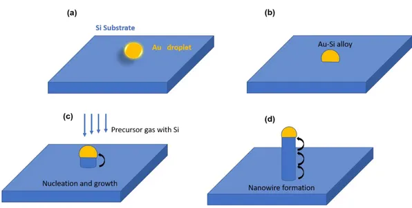
The first form of semiconductor NW-like structure was observed by Wagner and Ellis in 1964 in the form of silicon whiskers through a new method of crystal growth from vapor precursors, which they called vapor-liquid-solid (VLS) growth mechanism.1 In their novel work, the authors grew Si whiskers using a metal impurity(catalyst), gold in their particular case. Au droplets were heated at 950oC on the surface of Si substrate forming an Au-Si alloy in liquid phase, then a precursor gas containing Si was introduced to this system. Si atoms in the precursor gas enter the alloy droplet, supersaturate the Au-Si alloy, and precipitate, displacing the liquid alloy from the substrate surface. This process continues and Si whiskers grow until all the Au is consumed or until the growth conditions are changed. In their paper, the VLS mechanism yielded Si whiskers with diameters in the micrometer range. VLS remains to this date a prominent technique for NW growth. Figure 1.1 shows the VLS growth schematic of semiconductor NWs using Au catalyst. In the following years, several strides have been made towards growing NWs of different sizes, crystal structures, and tunable properties.2–7 The main push towards the development of NW-based research comes after the growth of III-V NWs by metal-organic vapor phase epitaxy in the early 1990s.8–10 Finally, by the late 1990s, NWs became a hot topic of research within the material science and nanotechnology community.11,12 NW growth techniques have also allowed the possibility of having semiconductor heterostructures with two or more materials growing on top of each other.13,14 NWs form heterostructures either with the substrate, meaning the NW and substrate are two different materials or as axial or radial heterostructures. In axial NW heterostructures, different materials are inserted or grown along the direction of the growth axis15, while radial heterostructures form core-shell like structures16. Heterostructures have an important application in bandgap tuning and surface passivation, as well as in the creation of axial and radial quantum dots in NWs.17
5
An important aspect, with technological consequences, is that the small size of the NW in contact with the substrate allows for efficient strain relaxation enabling growth on lattice-mismatched substrates, which is difficult in the case of thin films.18–20 Semiconductor NWs can also be doped using different impurities to control the minority (majority) carrier type, conductivity, and optical bandgap. In-situ doping of NWs can be done during the growth of the NWs by introducing impurities during the growth.21 A thorough study on the doping of semiconductor NWs can be found in the doctoral thesis of J Wallentin.22 All these interesting properties make NWs an important topic of research both in the field of technological applications as well as to study new physics concerning the 1D structure. Figure 1.2 shows the data obtained from the ISI web of science search engine using the keyword “nanowires”; it shows the tremendous growth in NW research in the last couple of decades.
Figure 1. 1. The schematic corresponding to the VLS growth of a Si NW starting with (a) a clean Si substrate with gold droplet deposited on it (b) which forms Au-Si alloy upon application of heat, (c) followed by introduction of precursor gases containing Si, during which the Si in vapor phase enters the Au-Si alloy leading to nucleation and growth, displacing liquid alloy from the substate surface, and (d) finally forming the long NW structure.
6
Another characteristic feature of semiconductor NWs is the existence of crystal structure polytypism.23 Polytypism is defined as “ a variant of polymorphism in which only periodicity along growth axis varies from one polytype to another leading to different crystal structures due to different unit cell extensions in the direction perpendicular to growth plane in which the periodicity (unit cell extension) is the same for all polytypes.”24 Semiconductors, belonging to group III-V, except nitrides, crystalize in the zinc blende (ZB) structure in bulk. However, when grown as NWs, they offer the possibility to exist also in the wurtzite crystal phase (WZ). Achieving different crystal phases is possible by changing the growth conditions. Polytypism has significant implications on the electronic and optoelectronic properties of the material. To truly understand the motivation behind studying NWs, a few problems faced by the current society and how NWs may be of help are discussed below:
1.1.1 The global climate crisis and how nanowires can help us
On the walls of the Metronome in Manhattan, USA there was a 15-digit electronic clock that showed the critical window for action to prevent the irreversible effects of global warming. This was installed by two artists Gan Golan and Andrew Boyd between the 19th to the 27th of September 2020. The time of this clock was updated based on calculations by the Mercator Research Institute on Global Commons and Climate Change at Berlin.25 As of 19th September 2020, there are about 7 years and 103 days remaining on this clock for us to take some solid actions against global warming. This Institute in Berlin also showcases the carbon clock on their website showing the time left until the CO2 budget is depleted. The carbon budget refers to the amount of CO2 the atmosphere can absorb if we want to limit global warming by 1.5 0C or 2 0C. As of 2018, the carbon budget we have in order to remain within the 1.5 0C limit was 9 years, and to remain within the 20C rise was 26 years.26 So, it seems like the right time,
Figure 1. 2.Number of publications on NW topics from 1995-2020 (Source of data: ISI web of science, keyword-"nanowires").
7
perhaps even a bit late, to find solutions to avoid the exhaustion of the carbon budget. And to do so, both political and technological strides must be made in the right direction. As scientists, we can work on improving the energy efficiency of existing technologies, as well as bring out new energy sources. This is where NWs might help us; in photovoltaics, hydrogen fuel economy, and energy storage.
Nanowire based solar cells
Solar energy is one of the most abundant and versatile forms of energy that is available on earth. However, due to limitations in the technology, only a small fraction of it is being used. As of 2018, around 505 GW of electricity was produced by solar photovoltaics, fulfilling a little more than 2% of the global electricity consumption. Figure 1.3 shows the renewable energy generation in the world as a function of time, obtained from Our world in data.27 Si solar cells based on a single p-n junction supply to the major solar energy demands in the world currently. Si solar panels can be expensive due to large material demands and can have energy losses due to fast carrier thermalization, and the inability to absorb all the photons, reflection, and non-radiative recombination of energetic carriers. This is where NWs could be of help.
Figure 1. 3. Chart showing breakdown of the renewable energy sources by their individual components over the years until 2019. As of 2019, Solar energy produced a total of 724.09 TWh.
8
The high surface area to volume ratio of NWs provides more photosensitive area for the same amount of material as compared to the thin film geometry. The versatile nature of NWs also helps to tune the bandgap and control the light absorption and scattering depending upon the dimension of the NWs.28–30Solar cell devices based on GaAs NWs have shown promising results in work done by Krogstrup et al.31 Similarly, InP NW based solar cells have also shown promising improvements.32
A more efficient type of solar cell is called Tandem solar cells, in which different materials with a range of bandgaps are stacked on top of each other. This helps efficient light absorption in different parts of the solar spectrum with the help of different bandgap materials. Such multijunction solar cells have shown efficiencies of about 38.8%.33 A problem in building tandem solar cells lies with the difficulty in growing materials on lattice-mismatched substrates. NW arrays can provide a solution here because of the ease with which NW based heterostructures can be grown.34
Photoelectrochemical water splitting for hydrogen fuel production
Hydrogen fuel created by splitting water using solar energy is a zero-carbon energy source. Though this will provide a great opportunity to help reduce greenhouse gas emissions, the efficiency of hydrogen production from solar energy has been quite low. Recently, some promising results have been displayed by nanowire-based photoelectrochemical water splitting electrodes. The large surface area to volume ratio provides more photon absorption as well as benefits through better carrier separation. Erik Bakker’s group at Eindhoven University have developed GaP NW based photocathodes.35 Photocathodes utilizing InP NWs with an efficiency of 6.4% have been demonstrated by Lu Gao et al.36 Similarly, several photoanodes with encouraging results based on NW structures have been developed recently. The main materials used in this case are TiO2 and ZnO. A detailed study of the optical properties of ZnO nanorods for photoanode applications is presented in chapter 5 of this thesis.
1.2 Need for characterization
NWs are becoming an important component in nanoelectronics device fabrication. Their unique structure allows NWs to exhibit several novel electronic, magnetic, optical, and thermal properties.31,37,38 For example, as the diameter of the NW reduces, the thermal conductivity of the NW decreases.39,40 NWs are being heavily researched for applications in solar cells,31,32,41,42 photoelectrochemical water splitting for hydrogen fuel,43–45 biosensors,46 field-effect transistors47 and several other nano-electronic devices. Perhaps one of the most interesting applications of NWs is their integration into nanophotonic devices. To integrate NWs into devices reliably, their properties must be thoroughly studied and understood. It is important not only to grow NWs efficiently but also to learn the basic physics that govern their fundamental properties. Carrier confinement, carrier concentration, the density of states, electronic band structure, carrier dynamics, optical absorption, light emission, etc. are some of the basic
9
properties that must be experimentally and theoretically studied before designing devices with the NWs. Apart from being a technologically versatile material system, NWs also provide an interesting setting to study several new and interesting physics. They are an ideal system to study how fundamental physics changes with size and dimensionality. Reliable characterization is therefore necessary for understanding the fundamental properties of these quasi-one-dimensional structures.
In this thesis, the optical properties of different semiconductor NWs are studied to understand their fundamental properties and to optimize them for device fabrication.
1.3 Types of characterizations
Various characterization techniques are required to optimize the growth of NWs and to control their properties. Characterization techniques also help to find out any possible defects as well as problems with the produced NWs. The following sections show some of the characterization techniques for NWs.
1.3.1 Structural characterization
To assess the quality of the NWs grown, two aspects must be characterized: electronic properties and structural properties. These two are closely connected to the growth parameters used. Out of the two, the structural properties are usually investigated first. As mentioned above, NW structures can show crystal structures different from the bulk depending upon the growth parameters. Another important aspect to be investigated through structural characterization is the presence of defects. Defect densities play an important role in determining the crystal quality, carrier concentration, and bandgap modification. Electron microscopies and X-ray diffraction techniques are commonly used to characterize the structural properties of NWs. The two common forms of electron microscopies are scanning electron microscopy (SEM) and transmission electron microscopy (TEM). SEM scans provide a resolution of about 1-10 nm while TEM scans can provide atomic resolution. Raman scattering is another very powerful tool to carry out the structural characterization of NWs. It is a non-destructive characterization technique that can give information on lattice strain, structural composition, phonon dispersion, etc.
1.3.2 Electrical characterization
The electronic properties of the NWs can be studied either through electrical characterizations or through optical studies. For electrical characterization, electrical contacts are required for the measurements. The most common method to perform this measurement is to remove the NW from the substrate, place it horizontally on an insulating substrate, and then connect
10
contacts on both ends of the NW. The contacts can be made using electron beam lithography. The conductivity is then measured by monitoring the current produced by sweeping with a source-drain voltage. Just as an example, Cui et al. have performed electrical transport in Si NWs using this method.48 However, preparing ideal contacts for these kinds of measurements can be challenging at times, and the contact resistance will have to be decoupled from the measurements.39 A way to reduce this problem is by using a 4-probe measurement in place of the 2-probe set-ups. For example, C. Thelander et al. have used a 4-probe method to accurately measure the resistivity of InAs NWs.49 Figure 1.4 adapted from C. Thelander et al. shows a 4-probe measurement setup on an electrically contacted InAs NW.
1.3.3 Optical characterization
Optical measurements constitute the non-destructive characterization techniques requiring comparatively less sample preparation. Since NW based solar cells and photonic devices are at the centre of NW research, it is necessary to understand their response to light excitation. The most common method of optical characterization is photoluminescence (PL).
1.3.3.1 Photoluminescence measurements
Steady-state and time-resolved (TR) PL can provide information about optical bandgap as well as carrier recombination times of materials. In PL the NWs are excited using a laser source
Figure 1. 4. A 4-probe electrical measurement setup on an InAs NW. Reprinted from C. Thelander et al [49], Copyright (2004) with permission from the Elsevier.
11
leading to the optical absorption of the photons by the carriers in the NW sample. The light emitted by the sample when the photoexcited carriers recombine is collected and analyzed. This gives information about the bandgap, the recombination mechanism, the presence of defects, etc. Through PL measurements, the steady-state of the semiconductor system is studied while TRPL measurements give information about the recombination rates. Depending on the band structure of the material, the PL efficiency varies. In a direct bandgap semiconductor, the valence band maxima and conduction band minima are at k= 0, while this is not the case in an indirect bandgap material. Therefore, in an indirect bandgap material the photon absorption leading to excitation of the electron to conduction band and recombination back to valence band are mediated by phonons because of momentum conservation rules. Hence, a direct bandgap material produces stronger and more efficient PL compared to an indirect bandgap semiconductor. Figure 1.5 shows the recombination process of carriers in the two cases.
The lifetime of a carrier is defined as the average time taken by the minority charge carriers to recombine after excitation. This quantity is dependent on the crystalline quality of the material, doping levels present, and other defects. The recombination process can be either radiative or non-radiative. The carrier lifetime can be expressed as,
1 𝜏 = 1 𝜏𝑟+ 1 𝜏𝑛𝑟 (1.1)
Figure 1. 5. Schematic diagram showing (a) direct bandgap and (b) indirect bandgap semiconductor with parabolic band structures. After absorption of a photon with energy greater than bandgap energy (blue arrow), excited carriers are created which thermalize to band edge by phonon emission (grey curly arrows). The red arrow shows the radiative recombination. For indirect bandgap, the absorption and emission are assisted by phonons.
12
where τ, τr, τnr are the average, radiative and non-radiative recombination lifetimes, respectively.
Depending on which component is the shortest, the most probable recombination method is determined. Non-radiative recombination can be further divided into (i) Auger recombination; (ii) defect mediated recombination, and (iii) surface recombination. Through TRPL measurements one can study the recombination lifetime of carriers in a material. This quantity is important in the functioning of light emitting devices, and hence it is crucial to know this value while choosing materials to design these devices.
Other common methods of optical characterizations include absorption, transmission, and reflection spectroscopies. With the advances in ultrafast laser systems, it has been possible to excite the NWs using ultrashort laser pulses and to probe the photoexcited sample with a precision of tens of femtoseconds or in some cases even attoseconds. Ultrafast spectroscopy of semiconductor NWs involves exciting the NWs using a pump laser with energy near or above the bandgap of the semiconductor. This photoexcited sample is then probed with a probe pulse at different time delays from pump excitation.
This thesis mainly focuses on the ultrafast spectroscopy of different semiconductor NW systems such as Si, InP, GaAs, and GaAsP NWs. ZnSe NWs functionalized with plasmonic nanoparticles (NPs) and cobalt doped ZnO nanorods (NRs) are also studied in detail. The motivations for studying those materials and material systems are given below.
1.4 Ultrafast spectroscopy of semiconductors
The development of ultrashort laser systems in the 7’0s began a paradigm shift in the optical characterization of materials. With the onset of ultrafast spectroscopic techniques, a whole regime of previously unexplored photoexcited carrier interactions came to the spotlight. Information regarding carrier dynamics, such as carrier-carrier interaction and carrier-phonon interaction is of extreme importance in device designing using NWs. This thesis deals with the ultrafast transient absorption (TA) spectroscopy in the pump-probe configuration. The detailed experimental setup is explained in Chapter 2. In TA spectroscopy, a pump pulse is incident on a small area on the sample. The interaction of the sample with pump pulse causes absorption, emission, transmission, reflection, and scattering of the photons. In the TA measurements, the significant processes are absorption, thermalization, and emission. After pump excitation, the probe light is incident on the same spot of the sample at different time delays, and by monitoring the pump induced changes in the absorption of the probe by the sample, information about photoexcited carriers is gathered. In this experiment, a quantity called differential absorbance of the probe light by the sample, ∆A is measured in milli OD. OD stands for optical density and is defined as the logarithmic ratio of the intensity of light incident on a material to the intensity of light transmitted by that material. It is a common unit used to measure the absorbance of a material. ∆A is obtained by measuring the intensity of the probe light transmitted through the sample with and without pump excitation. The absorbance A and the differential absorbance ∆A are defined as,
13 𝐴 = − log(𝑇) = −log (𝐼
𝐼0) (1.2)
∆A = −log (∆T
𝑇 + 1) (1.3)
where I and I0 are transmitted probe intensity with and without pump excitation, respectively. In an unperturbed semiconductor system, carriers and phonons remain in thermal equilibrium, with their average momentum equaling zero and average energy corresponding to the thermal energy of their common temperature. When an external force (field) is applied to the system, the carriers and phonons are perturbed. These perturbations lead to the excitation of carriers to higher energy states. The carriers at this stage can have energies much higher than the energy corresponding to the temperature of the lattice. Then through various scattering processes, the system relaxes to the equilibrium. In fast transient absorption spectroscopy (FTAS), after pump excitation, the electrons are excited from the valence band to the conduction band and the carrier dynamics of the photoexcited sample can be approximately divided into four temporally overlapping regimes:50
1. Coherent regime: This takes place within the first ~200 fs of the pump excitation. Several interesting phenomena such as carrier-carrier scattering, momentum scattering, and hole-optical phonon scattering take place in the coherent regime. The coherent phase follows immediately after pump excitation, where the carriers are still in phase with the electromagnetic wave that perturbed the system. This regime is of fundamental importance in the relaxation process of photoexcited carriers and manifests several quantum mechanical phenomena. As examples of work done on bulk semiconductor in this regime, I would like to point out the work of Q. T. Vu et al.51who have predicted an electron-plasmon quantum kinetics in bulk GaAs with 13 fs pulses at 300 K in this regime, and R. Huber et al.52 who have used pump-probe terahertz spectroscopy to measure buildup time for phonon-plasmon coupling.
2. Non-thermal regime: This regime is within the first picosecond after the photoexcitation by the short pump pulse. Here the dephasing of the coherent regime takes place leading to a non-thermal distribution of photoexcited carriers. In this phase various scattering processes like carrier-carrier and carrier-phonon scatterings take place, taking the system to a thermal distribution of the carrier energy, that can be defined by a carrier temperature. This regime is governed mainly by Coulomb interactions.
3. Hot-carrier regime: This regime is between 1 ps – 100 ps. After the scattering processes in the non-thermal regime, the carriers redistribute their energies and form a thermal distribution that is defined by a carrier temperature (Tc). This temperature is usually higher than lattice temperature (TL), and in the hot carrier regime, the carriers interact with phonons to cool down to the TL. This process can lead to a buildup of a large non-equilibrium distribution of phonons. This regime concerns with the hot carrier-phonon interaction, decay of the optical phonons leading to the creation of acoustic phonons, carrier-acoustic phonon scattering, and intersubband scattering. Studying the hot carrier
14
regime is of extreme importance while designing devices such as solar cells where there is a need to sustain hot carriers for longer times.
4. Isothermal regime: This regime is after about 100 ps from pump excitation. At the end of the hot carrier regime, thermal equilibrium is established between carriers and phonons, and with the same temperature as the lattice temperature. At this stage, there is an excess of electron-hole pairs, which then recombines radiatively or non-radiatively. The recombination times can be studied using TRPL measurements. Recombination can also take place involving electrons or holes trapped by defect states. At high carrier densities, another kind of recombination is possible called Auger recombination. It involves two conduction band electrons such that when an electron in the conduction band and a hole in the valence band recombine, the energy of the recombination is transferred to another electron in the conduction band, and that electron gets excited to a higher energy state in the conduction band.
It is important to understand that many of these processes can temporally overlap. This work is mainly concerned with the hot carrier regime, and the isothermal regime. The hot carrier regime is of particular interest while studying NWs because depending on the kind of device one must design, the prolonged sustainability of hot carriers or faster cooling of them is desired. For example, in a photovoltaic device, some of the energy absorbed is lost through cooling of the hot carriers, and in this case, it is preferred to collect the hot carriers prior to their cooling.53
1.4.1 Hot carriers
After the non-thermal regime, various carrier-carrier scattering processes allow the energetic non-thermal carriers to achieve a common temperature Tc in few picoseconds after photoexcitation. These carriers are called hot carriers because their distribution function is defined by Tc, where Tc>TL. In the hot carrier regime, the phonon and further carrier-carrier scatterings lead to the cooling down of hot carrier-carriers to the lattice temperature. By exciting the semiconductor with ultrashort pulses, and probing with a pulse at different time delays, cooling curves as a function of the time delay can be obtained. Throughout this thesis, in order to calculate the carrier temperature, a few assumptions are made: (i) parabolic band structure, (ii) Maxwell Boltzmann distribution for carriers whose Tc>TL, and (iii) the density of states does not vary substantially within the analyzed region of the spectra. In order to give an example of what I am writing about, I report the work by M. B. Price et al., who have shown carrier cooling in perovskites using TA measurements. Figure 1.6 taken from this work shows the determination of cooling curves through TA measurements.54
15
By fitting the high energy tail of the TA spectra with a Maxwell-Boltzmann distribution, one can find Tc at different delay times. In this way, the cooling curves as a function of time can be determined, and hence the rate of loss of energy in the hot-carrier regime can also be evaluated. For polar semiconductors, the energy loss is mainly due to interaction with optical phonons. The average rate of loss of energy is given by,47
< 𝑑𝐸 𝑑𝑡 > = ( ħ𝜔𝐿𝑂 𝜏𝐿𝑂 )exp ( −ħ𝜔𝐿𝑂 𝑘𝐵𝑇𝐶) (1.4)
where ħ𝜔𝐿𝑂 is the LO phonon energy, 𝜏𝐿𝑂 is the LO phonon scattering time and 𝑘𝐵 is Boltzmann constant. 1
𝜏𝐿𝑂 gives the scattering rate for the polar optical phonon. The value of this
scattering rate for bulk semiconductors is given by, 1 𝜏𝐿𝑂 = 𝑒2√2𝑚ħ𝜔𝐿𝑂 4𝜋ħ2 ( 1 𝜀∞− 1 𝜀0) (1.5)
where 𝜀∞ and 𝜀0 are the optical and static dielectric permittivity, respectively. By calculating carrier cooling rates in semiconductor NWs, we can have an idea about the phonon scattering times in different materials, as well as in NWs of same material with different sizes. This study has been carried out in this thesis for InP NWs and GaAsP NWs of two different diameters, as reported in Chapter 4.
Figure 1. 6 Normalized TA spectra at different time delays for lead iodide perovskite, with inset showing fits to determine carrier temperature of the hot-carrier distribution; (b) Carrier temperature as a function of delay time for different carrier densities. Figure adapted from M. B. Price et al. [54] with permission from the publisher.
16
Carrier-phonon interactions are crucial for semiconductor-based devices. Several works have been carried out to measure carrier cooling rates in bulk and thin-film semiconductors. However, only a few reports have been made on the carrier cooling rates in semiconductor NWs. Yong et al.55 have investigated the dynamics of hot carriers in InP NWs of WZ crystal structure with heavy ZB inclusions using transient luminescence and photoconductivity measurements. By approximating the high energy tail of transient PL of InP NWs with a Maxwell-Boltzmann distribution of the form proportional to exp(-E/(kBTc)) they obtained Tc at different time delays for NWs of diameter 50 nm and 160 nm. It is worth mentioning that Yong et al 55 discuss their results in terms of stacking faults whose density depends on the NW diameter. They do not relate Tc and cooling rate directly to the diameter values. They find that Tc is greater for 50 nm NWs compared to 160 nm NWs. They conclude that the NWs with higher stacking defect density can sustain carriers at a higher temperature. Figure 1.7 adapted from their work shows Tc as a function of delay time, and the rate of energy loss as a function of Tc in the inset.
In Figure 1.7 the carrier cooling rates slow down on crossing 750 K. This is due to a phenomenon called phonon-bottleneck. Phonon bottleneck can be of two types, optical phonon bottleneck or acoustic phonon bottleneck. Photoexcited carriers in polar semiconductors lose energy through interaction with optical phonon modes. At high excitation intensities, the cooling rate of hot carriers can decrease due to the buildup of a non-equilibrium population of hot longitudinal optical (LO)-phonon modes in the Brillouin zone center. These hot phonons cannot equilibrate effectively fast, leading the carriers to reabsorb the phonons and reheat. This is called the LO-phonon bottleneck.56 The LO-phonons that are produced in the initial part of carrier cooling further cools down by decaying into two counter-propagating longitudinal acoustic (LA)-phonons. At longer time delays, the cooling rates decrease significantly due to a non-equilibrium buildup of acoustic phonon modes by the decay of LO-phonons in the zone
Figure 1. 7.TC as a function of delay time for InP NWs of diameters 50 nm
and 160 nm. Inset shows the rate of energy loss as a function of TC. The measurements are done for two different initial carrier densities. Adapted with permission from Yong et al. [55] Copyright (2013) American Chemical Society.
17
center, called acoustic phonon-bottleneck.57 The strong decrease after 750 K in Figure 1.7 is due to the acoustic-phonon bottleneck.
Tedeschi et al.58 present another interesting work on the nature of long-lived hot carriers in III-V NWs. In their work, which has motivated my work on GaAsP NWs of different diameters, the authors have studied InP and GaAs NWs of ZB, WZ, and a mix of ZB and WZ crystal structure, with diameters varying from 61 nm to 700 nm. In that work, the authors use continuous-wave PL measurements to detect hot carriers, that thermalize at a higher temperature than the lattice temperature (TL). They defined a quantity ∆T, where ∆T = TC -TL, which increased with decreasing diameter independent of material, and morphology. Another observation was that in NWs with smaller diameters the hot carriers did not efficiently thermalize within few picoseconds. The peculiar aspect of their results was that the hot carriers were detected by steady-state PL measurements. The inefficient cooling down of hot carriers in thin NWs was attributed to the large-surface-to-volume ratio that prevents the cooling down of carriers to TL via the emission of phonons. The sustained presence of hot carriers in thin NWs have significance for photovoltaics and thermoelectric applications. Figure 1.8 adapted from Tedeschi et al.58 shows the difference of TC extracted from PL spectra and TL as a function of sample diameter.
Another important field where carrier-phonon interactions play a crucial role is in thermoelectric devices. So far, I have discussed optical measurements to study the scattering events involving phonons. Phonon scattering plays an important role also in the thermal
Figure 1. 8. ∆T = Tc -TL as a function of diameter for InP and GaAs
NWs grown by different mechanisms, as well as having different crystal structures. The inset shows diameters in nm for different samples. Adapted with permission from Tedeschi et al. [58]. Copyright (2016) American Chemical Society.
18
conductivity of NWs. Li and co-workers40 have investigated the diameter dependent thermal transport in Si NWs. They have carried out experiments on Si NWs of varying diameters from 22 nm to 115 nm and observed that the thermal conductivity was about 2 order of magnitude lower than that of bulk Si and the thermal conductivity reduced as the NW diameter decreased. The changes are assigned to possible changes in the phonon-dispersion relation as well as due to increased phonon-confinement due to the small diameter of NWs leading to different boundary conditions for the phonon scattering events. Similarly, Swinkels et al.39 report the diameter dependence of thermal conductivity of InAs NWs. They studied NWs with a range of diameters between 40-1500nm and found that the thermal conductivity reduced by 80% with respect to the bulk for a NW of 40 nm diameter.
In the following section of this chapter, a brief introduction to different materials studied in this thesis is given along with the motivation for their study.
1.5 Systems under study
NWs of different semiconductors were studied in this thesis with the common aim of understanding their response to light excitation. The first material under study is Si NWs, which is an indirect bandgap material. This is followed by ultrafast spectroscopy of NWs of group III-V, particularly InP, GaAs, and GaAsP. In the final chapter, two kinds of functionalization of semiconductor NWs are studied: (i) the effect of metal plasmonic NPs deposited on the sidewalls of ZnSe NWs, and (ii) Co-doped ZnO NWs.
1.5.1 Silicon nanowires
Si is an indirect bandgap semiconductor, with a bandgap value of about 1.1 eV and a direct bandgap of 3.3. eV. Si NWs were the first ones grown by VLS growth in 1964.1 Si is a robust material for technological applications due to its abundance and low cost. To date, Si is the most widely used semiconductor in the world. The entire world of information technology revolves around the developments in the miniaturization of Si-based integrated circuits (ICs). These ICs pack several Si-based transistors in them. Following Moore’s law59, the number of transistors in an IC has been doubling roughly every two years. The size of the Si components has shrunk so much that now the technology is transitioning to the quantum realm. Hence, it is imperative to study Si in its quantum regime. Si is currently the leader in solar cell production in the world.60 This demands a comprehensive study of the carrier dynamics in Si structures after photoexcitation.
The NWs used in this thesis are grown by plasma-enhanced chemical vapor deposition (PECVD). Chapter 3 deals with the ultrafast spectroscopy of Si NWs with a pump (2.34 eV) whose energy is lower than the direct bandgap energy of Si. After pump excitation, a white light supercontinuum probe in the visible region is used to study the changes induced by pump excitation near the direct bandgap transition. By comparing with the results of FTAS on Si NWs with pump energies above the direct bandgap energy, this thesis aims to disentangle the electron dynamics and hole dynamics. The diameters of the NWs grown by PECVD are too
19
large to observe any quantum effects. To study the effects of quantum confinement in NWs, experiments were planned on ultrathin Si NWs. However, due to the ongoing CoVid-19 crisis, this study has not been brought to its completion. Preliminary results on the ultrafast spectroscopy of ultrathin Si NWs with diameters less than 10 nm are presented. This final part is done as an introduction to the world of quantum confinement and related processes in ultrathin Si NWs.
1.5.2 Group III-V semiconductor nanowires
Chapter 4 deals with the ultrafast spectroscopy of group III-V semiconductor NWs. The first two materials: InP and GaAs are two widely studied direct bandgap semiconductors. Their thermodynamically stable crystal phase is ZB in the bulk state. However, in NW form they also crystallize in WZ state, impacting the optoelectronic properties. InP and GaAs are highly sought-after materials for photovoltaic materials. According to the efficiency curve calculated by Shockley and Queisser in1961 for the maximum light to electronic conversion efficiency for a single p-n junction solar cell, the bandgap of GaAs and InP falls in the energy range for maximum efficiency. Figure 1.9 taken from the work of Sven Rühle61 shows the maximum efficiency according to Shockley-Queisser curve62 as a function of bandgap energy, and one can see that InP and GaAs are ideal materials for photovoltaic applications. Figure 1.9 has a correction according to new data, where perovskites now show efficiencies > 25%.33
The final part of this chapter on III-V semiconductors deals with the study of hot carrier cooling in GaAsP NWs of different diameters. In this section, the rate of loss of energy by hot carriers in GaAsP NWs of different diameters is also deduced. This work is of particular interest because through ultrafast TA measurements, direct evidence for the diameter dependence of carrier cooling in NWs is observed. The novelty of this work is that it is done on NWs using an ultrafast TA spectroscopy that allows the determination of the scattering rates in NWs of
Figure 1. 9. Light to electric power conversion efficiency for a single p-n junction solar cell, when illuminated with 1.5 G irradiance as a function of bandgap. Reprinted from [61] Copyright (2016), with permission from Elsevier.
20
different materials and diameters. To obtain the results, the III-V NWs were transferred onto a transparent substrate, both by mechanical rubbing and by drop-casting with an organic solvent.
1.5.3 ZnSe nanowires decorated with metal nanoparticles
Chapter 5 is divided into two parts that deal with two different kinds of NW functionalization. The first part of the chapter studies the changes induced by Ag metal NPs on the optical properties and carrier dynamics of ZnSe NWs when deposited on its sidewalls. The local surface plasmon resonance (LSPR) of Ag NPs and the optical bandgap of ZnSe NWs overlap spectrally leading to resonant electronic interactions between the two. Low-temperature luminescence measurements and ultrafast spectroscopy are carried out on the Ag-decorated and pristine ZnSe NWs to study the plasmon-induced changes in optical properties. To understand the importance of the resonant condition between metal NP LSPR and semiconductor bandgap, ZnSe NWs were also decorated with Au NPs. The Au NP LSPR does not overlap with the bandgap of ZnSe NWs. By contrasting the results of Ag-decorated ZnSe NWs with Au-decorated ZnSe NWs, the importance of the resonant condition can be understood.
1.5.4 Cobalt-doped ZnO nanowires
ZnO is an abundant, thermodynamically stable, and wide bandgap material that is very promising in applications for photoelectrochemical (PEC) water splitting. The final part of Chapter 5 presents the controlled modification of the optical properties of ZnO NRs as a function of Co-doping. The samples with different doping levels were studied using cathodoluminescence and ultrafast spectroscopic techniques. PEC measurements are also presented to show the efficiencies as a function of doping levels. This allows for studying the correlation between changes in optical properties due to doping and the corresponding changes in the efficiency as a photoanode material. The application driver for this study is the usability of Co-doped ZnO NRs as PEC water splitting photoanodes. Once the optimal Co-doping concentration is determined, these NRs are further functionalized with the help of a metal-organic framework (MOF) around them forming a core-shell structure. These core-shell NRs are then characterized using the same techniques.
21
Chapter 2
Experimental techniques
During this thesis work, I have used several optical characterization techniques to study the steady-state and transient optical properties of semiconductor NWs. This chapter provides a brief review of the experimental techniques and set-ups used in this thesis. Although several techniques are used, the ultrafast pump-probe technique is the main experimental method used throughout this thesis.
2.1 Fast Transient Absorption Spectroscopy
Ultrafast spectroscopic techniques make use of an ultra-short, strong pulse of the laser, usually in the femto- to attosecond time range, to perturb the carrier distribution in a sample. This sample is then investigated by a probe pulse to study the photoinduced processes due to the pump excitation. Using a pump-probe setup (sketched in Figure 2.1), we can systematically study the temporal evolution of the photoinduced changes by varying the time delay between the pump and the probe using an optical delay line. In this way, one can investigate the temporal evolution of the spectra as well as the wavelength dependence of the characteristic times of the processes involved in the carrier dynamics.
Developments in ultra-short laser pulse generation have significantly improved the field of ultrafast spectroscopy.63,64 The two common sources of ultrashort laser pulses are Ti-Sapphire laser and the Yb doped crystal fiber laser.65 The Ti- Sapphire lasers provide lasing around 800 nm with pulse durations as short as ~20 fs. In this work, we have used a mode locked
Ti-Figure 2. 1. Schematic representation of a pump-probe experiment.
22
Sapphire laser, based on the Coherent Vitara-T oscillator system, with a frequency of 80 MHz, 20 fs short pulses and a power of 550 mW. This pulse is then amplified using a regenerative amplifier to produce output at 800 nm with a pulse length of ~ 35 fs at 1 kHz, and pulse energy of 4 mJ. The output of the regenerative amplifier is divided into two: a major part of the output goes into an Optical Parametric Amplifier (OPA). The OPA allows us to tune the pump wavelength from 240 nm to 20000 nm, with a pulse length of 35 -40 fs with a repetition rate of 1 kHz. A very small part (3µJ) of the output of the regenerative amplifier is used to produce the probe. The probe is usually kept at a very low power to prevent sizeable perturbations in the sample.
23
Figure 2.2 presents the schematic of the FTAS setup. The pump-probe experiments are performed using a commercial femtosecond transient absorption spectrometer (FemtoFrame II, IB Photonics). The tunable output from the OPA acts as the pump and is depicted by the blue ray in Figure 2.2. The tunable output from OPA allows the user to choose the pump energy according to the system that is being measured. The functioning of the OPA is described in Appendix A.1. The pump enters the spectrometer through the optical port W2 and after entering the spectrometer it first passes through a chopper (CH), and then into a telescope composed of two lenses that help focus the spot size of the pump on the sample. The M16 mirror helps to move the pump spot such that it can be aligned with the probe spot on the sample. The red ray shown in Figure 2.2, entering the spectrometer through the port W1 is the low power portion of the 800 nm laser. Immediately after entering the spectrometer, the 800 nm light is reflected from a flat mirror M1, and passes through a delay line, that helps to control the time delay in the pump-probe experiments. After this step, the 800 nm beam is directed using M2 and M3. A small portion of the light is passed through M3 to a photodiode for synchronization. F2 is a neutral density filter that helps to control the amount of the 800 nm light that goes into the white light generation. The beam is then focused using the M4 concave mirror into a rotating CaF2 crystal which produces a supercontinuum in the spectral range of 350 - 800 nm. The white light supercontinuum is focused using another concave mirror M5. After this, using a beam splitter (BS), the white light probe is split into two, in which 50 % of the white light passes through the BS and is used as a reference to account for pulse-to-pulse variations to give better signal to noise ratio, and the reflected half is directed to mirror M9 that reflects it to a collimating mirror M10, which focuses the probe on the sample. The reference beam reflects through flat mirror M8 and is collimated using L3 into an optical fiber that takes it to spectrograph 2 for detection. The intensity that enters the fiber is controlled by neutral density filter F4. An IR supercontinuum probe (800-1600 nm), obtained using a YAG crystal, is also available for TA experiments. After passing through the sample, the pump beam is blocked from entering the spectrograph by a beam blocker shown in Figure 2.2 as B, while the probe beam can be recorded either in transmission or reflection. Probe reflection from the sample is focused by concave mirror M11, while probe transmitted through the sample is reflected by mirror M12. Mirror M13 is a flip mirror to be used while measuring in reflection. F6 is a neutral density filter that helps to control the intensity of reflected/transmitted probe entering the fiber after being focused by L4 and taken to spectrograph 1 for detection.
During the measurement, the pump and the probe are focused on the same spot on the sample. The pump is chopped off at a reference frequency with a controlled time delay after pump pulse. In the visible range, two spectrometers simultaneously measure the reference probe and the probe that passes through the sample. Because of this dual probe beam setup, signals are collected through a two-step process. The probe and reference probe are recorded at each step with the chopper or shutter on and off, hence giving probe values with pump on and pump off. The two probe beams simultaneously pass through two different spectrographs and get dispersed by monochromators before being detected by CCDs. Since we measure the probe transmitted through the sample, the absorbance, A is defined in terms of transmittance, T as follows:64,66
24
The measured quantity is the difference in absorbance (∆A) of the probe transmitted through the excited sample and that transmitted through the unperturbed sample as a function of the delay time between pump and probe, and probe wavelength (energy), given by:
∆𝐴 = 𝐴𝑃 − 𝐴0 (2.2)
where Ap is the absorption with pump and A0 is absorption without pump excitation. Therefore, ∆𝐴 = log (𝑇0
𝑇𝑃) (2.3)
where T0 is the transmittance of probe pulse without pump excitation and TP is the time-dependent transmittance with pump excitation. This can be defined in terms of probe intensities as, ∆𝐴 = log (𝑇0 𝑇𝑃) = log ( 𝐼𝑃𝑟0 𝐼𝑅𝑒𝑓0 𝐼𝑃𝑟𝑒𝑥𝑐 𝐼𝑅𝑒𝑓𝑒𝑥𝑐 ⁄ ) (2.4)
where the lower index shows if it is probe (pr) or reference (ref), and upper index denotes if with pump excitation, i.e., with chopper open (exc) or without pump excitation i.e., with chopper closed (0).
An important aspect to keep in mind while acquiring TA spectra is something called chirp. This feature is introduced in the probe because of the temporal dispersion experienced by different spectral components of the white light continuum. For this reason, different spectral components enter the sample at slightly different time delays (<1 ps). A chirp correction must be made on all acquisitions to bring the data to a common zero before analysing the data. The figure below shows the TA spectra before and after chirp correction.
Figure 2. 3 2D false colourmap of FTAS spectra of a sample with wavelength along x-axis and time delay along y-axis, (a) shows the spectra with chirp, and (b) shows the spectra after chirp correction. After chirp correction, the zero is the same for all wavelengths.
25
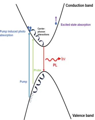
The TA spectra can have either positive or negative values for the ∆A depending on absorption of probe light by the photoexcited sample. A negative ∆A is indicating that the probe light can pass through the sample being less absorbed by the photoexcited sample compared to unexcited sample. This happens because the pump excitation causes the depopulation of the valence band in the semiconductor. A negative ∆A due to photoexcitation of carriers due to pump from the valence band to the conduction band is called an absorption bleaching. A positive ∆A corresponds to the increase in absorption of the probe. Figure 2.4 shows the schematic of different pump induced processes in a direct bandgap semiconductor. One of the examples where the ∆A is positive is the intraband free carrier absorption.
In this work, I have used different pump energies depending on the material system under study. The samples have been probed using the IR and visible probe as needed. The measurements in this work are done in transmission mode. The samples have been measured both at room temperature and some samples also at 77 K using a liquid nitrogen cooled cryostat.
Figure 2. 4. Schematic of different pump induced processes in a direct bandgap semiconductor.
26
2.2 UV – Visible Spectroscopy
UV-Vis spectroscopy is one of the most widely used tool for the optical characterization of different materials. Using an UV-Vis spectrometer one can measure the intensities of absorbed, transmitted, or reflected light as a function of wavelength from UV to near IR. In this thesis, I have used a Perkin-Elmer Lambda 35 spectrometer for measuring the static absorption of different NW samples. The instrument has a working range from 190 nm to 1100 nm with a double beam configuration allowing reference to be measured and corrected in real time.
2.3 Steady state and time resolved photoluminescence
PL is an optical property of materials in which light is emitted after the absorption of photons. PL spectroscopy is an important tool for studying the optoelectronic property of materials because of its non-destructive nature. During optical absorption in semiconductors, typically involving incident photons with energy greater than the bandgap energy, the electrons get excited from the valence band to the conduction band, leaving a hole in the valence band, thus creating a non-equilibrium distribution of electron-hole pairs. The excited carriers cool down to the respective band edge and finally recombine, radiatively or non-radiatively. In the radiative case, the recombination energy is emitted as a photon. For direct gap semiconductors, in momentum space, the transition occurs at k=0. In this case, the probability of radiative recombination is high, with important applications in light emitting devices.67,68 In the case of indirect bandgap semiconductors, the transition is not vertical in the energy versus momentum dispersion relationship. Hence, it involves phonons as a momentum conserving agent. In this case, the radiative recombination is less efficient. Si is an example for such a material.69 In this work, PL spectroscopy is carried out both at room temperature and at low temperatures down to 10 K with the help of a closed cycle He cryostat. The cryostat operates in vacuum with the help of a turbo pump. A PID temperature controller is also connected to the cryostat to measure PL at all intermediate temperatures between room temperature and 10K. The samples are excited using a continuous wave (CW) laser at 405 nm supplied by the Matchbox 2 laser series or pulsed laser from the second harmonic generation (SHG) from the mode locked Ti-Sapphire laser (800nm, 80 MHz) at 405 nm. The laser is focused on the sample, and the luminescence from the excited sample is collected and sent to the monochromator. The monochromator is the HORIBA Jobin Yvon – iHR320. The monochromator has a focal length of 320 mm, and a spectral range of 350 nm -1100 nm with 1200 gr/mm grating.
27
The monochromator consists of the entrance slit with a height limiter through which the collected light is sent to a collimating mirror. From the collimating mirror the light is incident on the diffraction grating turret which sends the signal to a focusing mirror. The focused signal is then sent to either to the charge coupled device (CCD) detector or to the single photon counting detector. The CCD collects the emitted signal and produces the PL spectra while the single photon detector based on a silicon single photon avalanche photodiode (SPAD) helps in time correlated single photon counting (TCSPC). The start time for time resolved measurements are triggered by a Si photodiode. Figure 2.5 shows the schematic of the PL setup. To measure high bandgap materials like ZnO, a pump greater than 3.1 eV was required. So, they were studied on a different system which used the OPA tuneable output as a pump. These measurements were done in a Halcyone ultrafast system. Halcyone also provided time-resolved PL measurements performed at room temperature with a time-correlated single photon counting (TCSPC) system with a photomultiplier as the detector with an instrumental response function (IRF) of 0.5 ns.

![Figure 3. 1. Schematic of the band structure of Si, taken from Fauchet, 2005 [78].](https://thumb-eu.123doks.com/thumbv2/123dokorg/2884927.10744/39.892.265.588.762.1082/figure-schematic-band-structure-si-taken-fauchet.webp)