Facoltà di Ingegneria
Dipartimento di Ingegneria dell’Informazione ed Elettrica e Matematica Applicata
Dottorato di Ricerca in Ingegneria dell’Informazione XIV Ciclo – Nuova Serie
T
ESI DID
OTTORATOControl Issues in
Photovoltaic Power
Converters
C
ANDIDATO:
M
ASSIMILIANODE
CRISTOFARO
C
OORDINATORE:
P
ROF.
M
AURIZIOLONGO
T
UTOR:
P
ROF.
N
ICOLAFEMIA
C
O-T
UTOR:
P
ROF.
G
IOVANNIPETRONE
Anno Accademico 2014 – 2015
UNIVERSITÀ DEGLI STUDI DI SALERNO
To my family
To my friends
Contents
Contents ... 3
Introduction ... 5
Chapter 1 Photovoltaic Inverters ... 10
1.1 Half-Bridge Voltage Source Inverter ... 11
1.2 Full-Bridge Voltage Source Inverter ... 12
1.3 Three-phase Voltage Source Inverter ... 13
1.4 Neutral point Clamped Inverter ... 14
1.5 αβ and dq transformations ... 16
1.6 Control techniques for PV inverters ... 20
1.7 Maximum Power Point Tracking techniques ... 25
References ... 29
Chapter 2 An improved Dead-Beat control based
on an Observe&Perturb algorithm... 31
2.1 Description of the simulator tool ... 33
2.2 Standard controller design ... 35
2.2.1 Proportional-Integral Linear Control design ... 38
2.2.2 Dead-Beat control design ... 40
2.2.3 Hybrid solution: Dead-Beat and integral action ... 45
2.3 Observe&Perturb Dead-Beat control ... 45
2.4 Simulation results ... 49
2.5 Implementation on a microcontroller ... 56
4 Contents
Chapter 3 The Effect of a Constant Power Load
on the Stability of a Smart Transformer ... 65
3.1 Constant power load characteristic and single loop
control analysis ... 68
3.2 Double loop control analysis ... 79
References ... 82
Chapter 4 Minimum Computing MPPT ... 84
4.1 Light-to-Light system case study ... 86
4.2 Adaptive duty-cycle setup ... 88
4.3 LED Dimming-based Bulk Voltage regulation ... 95
4.4 Experimental results ... 98
References ... 107
Conclusions ... 109
List of publications ... 112
Introduction
The development of this thesis was born from cooperation between the Power Electronics and Renewable Sources Laboratory of the University of Salerno and the ABB Solar Group company (ex
Power-One) of Terranuova Bracciolini (AR), Italy that is one of the most
important manufactures of Photovoltaic (PV) power converters. Its portfolio covers all the possible PV systems: from the module (50-400W), to the string (0.2-2kW) up to the centralized solutions (more than 1MW).
This company has pointed out a great interest to investigate issues related to the control of PV systems to explore new control techniques that can have static and dynamic performance better than the existing techniques implemented in its systems, to analyze new scenarios due to the insertion of the Distributed Power Generating Systems (DPGSs) into the grid and to optimize the current methods to extract power from the PV source with the final goal to increase the performance of the PV systems at any level, system, grid and circuit. Specifically the progress of photovoltaic technology has opened a scenario of different solutions:
- at system level, still today there is a high interest of the industry for the centralized solutions in less-developing country, such as China, India and Thailand, where the system must work in poor grid conditions with great changes of frequency and root-means square value and must be able to ensure the respect of the regulation requirements during the grid faults. So, define new current control techniques that allow having better performance for these systems is currently a challenge for the industry;
- at grid level, it has enabled a transition from a highly centralized structure of electric power system, with large capacity generators, to a new decentralized infrastructure with the insertion of small and medium capacity generators. This has led great changes in the electric grid. The conventional
6 Introduction grid was composed of a source, a distribution energy system and loads. Instead, new scenarios include the presence of DPGSs that can inject locally energy into the grid. The study of DPGSs is of a great interest from the point of view of the overall system, where it is important to choice where it is convenient to insert the DPGS, as well as from the point of view of the local system, where there are problems to control and synchronization. Moreover, the increase in performance, combined with the costs reduction of solid state devices, has led to the development and the diffusion of the power converters with the result that, today, almost the totality of the electrical energy is controlled by power electronic systems;
- at circuit level, the wide interest for Maximum Power Point Tracking (MPPT) control is justified by the attempt to maximize the energy harvested from photovoltaic sources in all the operating conditions. Several control techniques can be adopted, both analog and digital, to achieve good MPPT efficiency. Digital techniques are best suited to implement adaptive control. The runtime optimization of MPPT digital control is in the focus of many studies, mostly regarding the Perturb&Observe (P&O) technique. The two parameters determining the MPPT efficiency and the tracking speed P&O technique are the sampling period TMPPT and the duty-cycle
step perturbation magnitude ΔD. The level of MPPT efficiency achievable by the most of the existing techniques is conditioned by many factors, such as the modeling assumptions, the duty-cycle and sampling period correction law adopted, the computing capabilities of the digital device adopted for the control implementation. To this regard, they involve a variable amount of computations, including the calculation of the ratios (e.g. ΔI/ΔD, ΔP/ΔV) used as figure of merit, the subsequent calculations required by the adaptation law, and the additional calculations required by specific estimation/decision algorithm used. As a consequence, many methods and algorithms yield high MPPT efficiency at the price of high computing effort, which is not compatible with low cost requirements. Achieving maximum energy harvesting
7 Introduction with minimum cost devices is a fundamental renewable energy industry demand.
Hence, there are many issues, also attractive for the scientific field, to investigate about the design of PV systems in the present-day evolving scenario, as it is not completely defined. For this reason, during this study, models, methods and algorithms will be developed to analyze these challenges at any level starting from the inputs provided by ABB Solar Group.
The dissertation is organized as follows.
In the chapter 1, the basic circuit topologies and tools used for the PV systems will be presented. The main aim is to explain the operation of circuits and tools used by ABB Solar Group for its converters and that will be used for the control issues analyzed in the next chapters. Hence, the basic Voltage Source Inverter (VSI), single-phase and three-single-phase, and the multilevel Neutral Point Clamped (NPC) inverter will be discussed. Also very useful tools for the control design, the αβ and dq transformations, will be summarized and, at the end, an overview of the existing control and MPPT techniques will be presented.
In the chapter 2, an improved Dead-Beat control based on an Observe&Perturb (O&P) algorithm will be developed for the Neutral Point Clamped (NPC) inverter that is the most widely used topology of multilevel inverters for high power applications. Indeed a NPC-based inverter, the AURORA ULTRA of 1.4MW, is developed by ABB
Solar Group mainly for the Asian market. A comprehensive
comparison between the standard Dead-Beat, the proportional-integral and the proposed Dead-Beat control will be performed for a passive NPC inverter. Also stability aspects for these controllers will be analyzed and, based on that, the general guideline to select the parameters of the proposed O&P algorithm will be defined. The comparison will be done with a dedicated simulation tool, written in C++ language, since the existing commercial software, such as Simulink®, PSIM® and PSPICE®, allow to make the analysis only a specific level: system, circuit or device. Both O&P method and simulation tool are not only for NPC inverters but they are very
8 Introduction general being able to be applied to all the converters. At the end, the proposed O&P Dead-Beat control will be implemented on a TMS320F28379D Dual-Core Delfino™ Microcontroller (µc) to test the feasibility of all its components in a single embedded system. The choice of the F28379D µc is carried out to use the same family, the TI C2000, that ABB Solar Group implements on its converters and to have the best performance with a dual-core system. This µc implementation has been performed at the Texas Instruments of Freising, Germany.
In the chapter 3, a critical scenario for the stability of the electric grid will be investigated. It will be implemented with a Smart Transformer (ST) that can be composed by one or more energy conversion stages, i.e. one or more power converters, some loads and some DPGSs directly connected to the low voltage side of the ST. The ST is a Solid State Transformer (SST) used in electric distribution system to provide ac bus voltages with a fixed amplitude and frequency for each of the possible configuration of loads. The international industry practice on load modeling for static and dynamic power system studies will be discussed and it will be shown that the Constant Power Load (CPL) model is mostly used (about 84%) for power system static analysis. The main characteristic of a CPL is that its current decreases when its voltage increases and vice versa and, so, it presents negative impedance for the small signal analysis that can impact the system stability. For this reason, in this chapter, the scenario with only CPLs, the worst case for the stability, will be analyzed to verify if it is possible to use controllers usually designed for stable systems even when the CPLs make the system unstable. A three-phase system, composed by a Voltage Source Inverter (VSI) with an LC filter representing the output stage of the ST, a DC-source that represents the ST DC bulk, the CPL, the controller and the Pulse Width Modulator (PWM) will be considered. At the end the conditions to design the LC filter to have a stable system with a CPL will be provided. The analysis of a system with a CPL has been developed also in cooperation with the Chair of Power
Electronics of the Albrechts-Universität zu Kiel, Germany.
In the chapter 4, after that the methodologies to track the Maximum Power Point (MPP) will be presented, a method to
9 Introduction determine the sampling period TMPPT and the duty-cycle step
perturbation magnitude ΔD will be developed. This realizes the real time adaptation of a photovoltaic P&O MPPT control with minimum computing effort to maximize the PV energy harvesting against changes of sun irradiation, the temperature and the characteristics of the PV source and by the overall system the PV source is part of. It exploits the correlation existing among the MPPT efficiency and the onset of a permanent 3 level quantized oscillation around the MPP. A comparison between an existing adaptive MPPT algorithm will be performed through simulations, to set exactly the same test conditions and, after, as a multifunction control application case study, a TMS320F28035 Texas Instruments Piccolo™ Microcontroller will be used to implement the proposed adaptive PV MPPT control algorithm on a 70W LED lighting system prototype fed by a photovoltaic source, with a capacitor working as storage device. The choice of the F28035 µc is carried out to use the same family, the TI C2000, that
ABB Solar Group implements on its converters but with a single-core
system as the goal of the proposed method is the minimum computing effort. Hence the aim of this chapter is to determine an optimize MPPT algorithm that can be implemented in the ABB Solar Group systems.
Chapter 1
Photovoltaic Inverters
The PV inverter is the main element of grid-connected PV power systems: it converts the power from the PV source into the AC grids. The development of the circuit topologies for the PV inverters has had as principal goal to maximize the efficiency but other complex functions, usually not present in motor drive inverters, are typically required like the maximum power point tracking, anti-islanding and grid synchronization [1]. To have an increment of the efficiency, the galvanic isolation typically provides by high-frequency transformers in the DC/DC boost converter or by a low-frequency transformer on the output has been eliminated. But the transformerless structure typically requires more complex solutions to keep the leakage current and DC current injection under control in order to comply with the safety issues resulting in novel topologies. These topologies have been taking the starting point from two converter families: H-bridge and Neutral Point Clamped (NPC) that are the most suitable respectively for low power inverter (up to tens of kW) and for high power inverters (hundreds of kW) [1].
The aim of this chapter is to explain the operation of the basic circuits, H-bridge and NPC, and to introduce very useful tools for the control design of these inverters, the αβ and dq transformations. Also, at the end, an overview of the exiting control and Maximum Power Point Tracking (MPPT) techniques is presented.
These circuits, tools and control techniques, all used by ABB Solar
Group in its converts, represent the starting points for the control
11 Chapter 1 Photovoltaic Inverter
1.1 Half-Bridge Voltage Source Inverter
The figure 1.1 shows the power topology of a half-bridge VSI [2], where two capacitors (C+ and C-) are required to provide a neutral
point N, such that each capacitor maintains a constant voltage vi/2.
Because the current harmonics injected by the operation of the inverter are low-order harmonics, a set of large capacitors is required.
It is clear that both switches S+ and S- cannot be ON
simultaneously because a short circuit across the dc link voltage source vi would be produced. There are two defined (states 1 and 2)
and one undefined (state 3) switch states as shown in the table 1.1. In order to avoid the short circuit across the dc bus and the undefined ac output voltage condition, the modulating technique should always ensure that at any instant either the top or the bottom switch of the inverter leg is ON [3].
Fig 1.1 Single-phase half bridge VSI
State vo Components Conducting S+ is ON and S- is OFF v+/2 S+ if io>0 D+ if io<0 S- is ON and S+ is OFF -vi/2 S- if io>0 D- if io<0
S+ and S- are all OFF vi/2
- vi/2
D+ if io>0
D- if io<0
12 Chapter 1 Photovoltaic Inverter
1.2 Full-Bridge Voltage Source Inverter
The figure 1.2 shows the power topology of a full-bridge VSI [2]. This inverter is similar to the half-bridge inverter but a second leg provides the neutral point N to the load. Both switches S1+ and S1- (or S2+ and
S2-) cannot be ON simultaneously because a short circuit across the dc
link voltage source vi would be produced. The table 1.2 shows the
possible five states of this circuit: four defined and one undefined. The modulation technique, ensuring that either the top or the bottom switch of each leg is ON at any instant, avoids the short circuit across the dc bus and the undefined ac output voltage condition. Looking at the tables 1.2 and 1.1, it is possible to notice that the ac output voltage for the full-bridge can take values up to the dc link value vi, while the half-bridge can reach vi/2. [3].
Fig 1.2 Single-phase full bridge VSI
State va vb vo Components Conducting
S1+ and S2- are ON and S1- andS2+ are OFF vi/2 -vi/2 vi S1+ and S2- if io>0
D1+ and D2- if io<0
S1- and S2+ are ON and S1+ andS2- are OFF -vi/2 vi/2 -vi S1- and S2+if io>0
D1- and D2+ if io<0
S1+ and S2+ are ON and S1- andS2- are OFF vi/2 vi/2 0 S1+ and S2+if io>0
D1+ and D2+ if io<0
S1- and S2- are ON and S1+ andS2+ are OFF -vi/2 -vi/2 0 S1- and S2- if io>0
D1- and D2- if io<0
S1+, S2+, S1- and S2- are all OFF -vi/2
vi/2 vi/2 -vi/2 - vi vi D1- and D2+ if io>0 D1+ and D2- if io<0
13 Chapter 1 Photovoltaic Inverter
1.3 Three-phase Voltage Source Inverter
The single-phase VSIs cover low-range power applications while the three-phase VSIs cover the medium to high-power applications (from few hundreds of kW) [2]. The main purpose of these topologies is to provide a three-phase voltage source, where the amplitude, phase, and frequency of the voltages should always be controllable. Although most of the applications require sinusoidal voltage waveforms, arbitrary voltages are also required in some emerging applications (e.g. active filters, voltage compensators).
The standard three-phase VSI topology is shown in the figure 1.3 and the eight valid switch states are given in the table 1.3 based on the same considerations for the single-phase VSIs described in the previous sections. Of the eight valid states, two of them (7 and 8 in the table 1.3) produce zero ac line voltages. In this case, the ac line currents freewheel through either the upper or lower components. The remaining states (1 to 6 in table 1.3) produce no-zero ac output voltages. In order to generate a given voltage waveform, the inverter moves from one state to another. Thus the resulting ac output line voltages consist of discrete values of voltages that are vi, 0, and -vi for
the topology considered. [3].
14 Chapter 1 Photovoltaic Inverter
State vab vb va
1. S1, S2 and S6 are ON and S4,S5 and S3 are OFF vi 0 -vi 2. S2, S3 and S1 are ON and S5,S6 and S4 are OFF 0 vi - vi 3. S3, S4 and S2 are ON and S6,S1 and S5 are OFF - vi vi 0 4. S4, S5 and S3 are ON and S1,S2 and S6 are OFF - vi 0 vi 5. S5, S6 and S4 are ON and S2,S3 and S1 are OFF 0 - vi vi 6. S6, S1 and S5 are ON and S3,S4 and S2 are OFF vi - vi 0 7. S1, S3 and S5 are ON and S4,S6 and S2 are OFF 0 0 0 8. S4, S6 and S2 are ON and S1,S3 and S5 are OFF 0 0 0
Table 1.3 Valid switch states for a three-phase VSI
1.4 Neutral point Clamped Inverter
The multilevel inverter has been developed to improve the performance of the two levels inverters and has become more and more interesting with the continuous evolution of the power switches in term of voltage and current rating and price [3].
A multilevel inverter that has the same voltages and powers of a two levels inverter has a better voltages harmonic spectrum so it is simpler to respect the law requirements. Indeed, having more levels, it is able to reproduce voltage and current waveforms more similar to a sinusoidal one and so the load absorbs fewer harmonic.
The principal effects of the harmonic reductions into the current loads are:
less power losses in the iron and copper less electromagnetic interferences (EMIs) less mechanical oscillations in motor loads
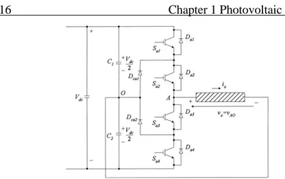
The Neutral Point Clamped (NPC) inverter is the most extensively applied multilevel converter topology at present [3]. A three-level NPC inverter is illustrated in the figure 1.4, which is able to provide five-level-step-shaped line to line voltage (three-level-step-shaped phase voltage) without transformers or reactors and so it can reduce harmonics in both of the output voltage and current. The main benefit of this configuration is that each of the switches must block only half
15 Chapter 1 Photovoltaic Inverter of the dc-link voltage Vdc even if their number is twice of a two-level
inverter. However, the NPC inverter has some drawbacks, such as additional clamping diodes, a complex Pulse Width Modulation (PWM) switching pattern design and a possible deviation of Neutral Point (NP) voltage. In addition, since the NPC inverter is mostly used for medium or high-power applications, the minimization of the switching losses is such a relevant issue. As to the modulation strategies, three popular modulation techniques for NPC inverters, Carrier-Based (CB) PWM, Space Vector Modulation (SVM) and Selective Harmonic Elimination (SHE), have been widely used in practice. The SHE method shows an advantage for high-power applications due to having a small number of switching actions. The other two PWM techniques are commonly used in various applications because of their high PWM qualities [3].
A leg of a three-level NPC inverter is shown in the figure 1.4 where it is possible to note the structural differences compared to the two-level inverter. A three-level NPC inverter has 4 switches (Sa1, Sa2,
Sa3, Sa4) and other 2 diodes (Dca1, Dca2) with the function to clamp the
output voltage as they are connected to the medium point of the DC bus between two equal capacitors. Hence, the possible Vao values are
Vdc/2 and –Vdc/2. The table 1.4 shows the switches states with a fixed
output voltage. It is worth noting that the control signal of Sa1 is in
opposite phase of Sa3 as well as the signal control of Sa2 is in opposite
phase of Sa4. The four switches cannot be ON or OFF at the same time
for the same reasons of the two-level inverters [4].
Three inverter legs in parallel can work independently making in the output the three sinusoidal voltages with 120 degrees of phase shift. In this topology, the reverse maximum voltage of the switches is Vdc/2 while for two-level it is Vdc. This leads to select cheaper
16 Chapter 1 Photovoltaic Inverter
Fig 1.4 Multilevel Neutral Point Clamped Inverter
State vAO Components Conducting
Sa1, Sa2 are ON and Sa3 and Sa4 are OFF Vdc/2 Sa1, Sa2 if io>0
Da1, Da2 if io<0
Sa2, Sa3 are ON and Sa1 and Sa4 are OFF 0 Dca1, Sa2 if io>0
Dca2, Sa3 if io<0
Sa3, Sa4 are ON and Sa1 and Sa2 are OFF - Vdc/2 Da3, Da4 if io>0
Sa3, Sa4 if io<0
Table 1.4 Switch states for a NPC inverter
1.5 αβ and dq transformations
When the three phase converter is characterized by four wires, i.e. three phases plus neutral, the application is straightforward since a four-wire three-phase system is totally equivalent to three independent single-phase systems [5]. In contrast, it would need to apply more caution when it is dealing with a three-phase system with an insulated neutral, i.e. with a three-wire three-phase system. The aim of this section is to give the basic knowledge needed to extend the control principles to this kind of systems. Two fundamental tools are required to design an efficient three-phase controller: the αβ transformation and the dq transformation.
The αβ transformation represents a very useful tool for the analysis and modeling of three-phase electrical systems. In general, a three-phase linear electric system can be properly described in mathematical terms only by writing a set of tridimensional dynamic equations (integral and/or differential), providing a self-consistent
17 Chapter 1 Photovoltaic Inverter mathematical model for each phase. In some cases though, the existence of physical constraints makes the three models not independent from each other. In these circumstances the order of the mathematical model can be reduced, from three to two dimensions, without any loss of information. As it is meaningful to reduce the order of the mathematical model, the αβ transformation represents the most commonly used relation to perform this reduction [5].
Considering a tridimensional vector xabc = [xa xb xc]T that can be
any triplet of the system electrical variables, voltages or currents, it is possible to introduce the linear transformation, Tαβγ:
1 1 1 2 2 2 0 3 2 3 2 3 1 1 1 2 2 2 a a b b c c x x x x T x x x x x (1.1)
which, in geometrical terms, represents a change from the set of reference axes denoted as abc to the equivalent one indicated as αβγ. The Tαβγ transformation has the following interesting property:
0 0
a b c
x x x x (1.2)
Every time the constraint (1.2) is valid for a tridimensional system, the coordinate transformation Tαβγ allows describing the same system in a
bidimensional space without any loss of information. Considering a triplet of symmetric sinusoidal signals:
sin sin 2 3 sin 2 3 a M b M c M e U t e U t e U t (1.3)18 Chapter 1 Photovoltaic Inverter
2 sin 3 2 cos 3 M M e U t e U t (1.4)and that the space vector, eabc, associated with (1.3), satisfies the
constrain (1.2) and so it can be described without loss of information in the αβ reference frame.
Hence the three-phase inverter is completely equivalent to a couple of independent single-phase inverters making the controller design of such inverter possible in the αβ reference frame and leading to an improvement of the performance as it will be shown in the chapter 4 of this work.
Another useful tool is the dq transformation that exploits the Park transform, a very well-known tool for electrical machine designers. While the αβ transformation maps the three-phase inverter and its load onto a fixed two-axis reference frame, the dq transformation maps them onto a two-axis synchronous rotating reference frame. This practically means moving from a static coordinate transformation to a dynamic one, i.e. to a linear transformation whose matrix has time varying coefficients.
The transformation defines a new set of reference axes, called d and q, which rotate around the static αβ reference frame at a constant angular frequency ω. The rotating vector angular speed equals the angular frequency of the original voltage triplet, which it is possible to consider the fundamental frequency of the three-phase system. If the angular speed of the rotating vector equals ω in the dq reference frame, the vector is not moving at all. Hence, the advantage is represented exactly by the fact that sinusoidal signals with angular frequency ω are seen as constant signals in the dq reference frame. This principle is exploited in the implementation of the so-called synchronous frame current control in the chapter 2, where the Park transform angular speed is chosen exactly equal to the three-phase system fundamental frequency.
The following matrix provides the mathematical formulation of the Park transform considering the equation (1.1):
19 Chapter 1 Photovoltaic Inverter cos sin sin cos d dq q x x x T x x x (1.5)
The two system dynamic equations are complicated by the cross-coupling of the two axes, i.e. they are no longer independent from each other. This is the reason why, decoupling feed-forward paths are usually included in the control scheme making the system dynamic totally identical to those of the original one.
To complete the discussion of the Park transform, it worth be noted that it is also possible to implement the so-called inverse sequence Park transform where the direction of the dq axes rotation is assumed to be inverted, while the transformation (1.5) can be identified as the direct sequence Park transform. This inverse transformation could be required when the system is unbalanced and asymmetrical as impedance unbalances and/or asymmetric voltage sources can be found. In this case, a three-phase system can be shown to be equivalent to the superposition of a direct sequence system and an inverse sequence system, both of them symmetrical and balanced and so both properly describable in the this reference.
Also, because the elements of Tdq are not time invariant, the
application of the Park transform, differently from the αβ transformation, affects the system dynamics: any controller, designed in the dq reference frame, is actually equivalent to a stationary frame controller that does not maintain the same frequency response.
20 Chapter 1 Photovoltaic Inverter
1.6 Control techniques for PV inverters
In the figure 1.5, the schematic grid-connected system representation is shown while the current control loop is considered in the figure 1.6 in order to analyze the error caused by the control of AC quantities in steady-state condition. LCL-filter Controller PWM i* i RL Lf Cf RC i DC Inverter Rg Lg Grid
Fig 1.5 Schematic grid-connected system representation
Fig 1.6 Current Control Loop
The variables shown in the figure 1.6 are as follows:
• e is grid voltage acting on the system as a perturbation • i* is the current reference for the current control loop • i is the measured grid current
• Δi is the error between the measured grid current and the current reference
• Gc is controller transfer function in the Laplace domain
21 Chapter 1 Photovoltaic Inverter • Gp is the plant transfer function in the Laplace domain, which
is usually composed by the output filter of the converter and the grid impedance
• v* is the controller output voltage
It has been demonstrated [6] that the grid connected LCL filter can be regarded as an inductance for low frequencies. So it is possible to define: 1 ( ) p G s Ls R (1.6)
where L and R are respectively the filter inductance and its parasitic resistance.
Indicating Ts the sampling time of a typical digital system, Gi is the delay due to elaboration of the computation device (typically 1Ts) and to the PWM (typically 0.5Ts) [1]: 1 ( ) 1.5 1 i G s Ts (1.7)
Hence, the current error produced by the perturbations e is:
( ) ( ) ( ) 1 ( ) ( ) ( ) p i c i p G s s e s G s G s G s (1.8)
The controller goal is to minimize the steady-state current error Δi(s). There are several strategies for the control of the AC current in the case of Distributed Power Generation Systems (DPGSs). A very common technique used for three-phase systems is the dq control, synchronous rotating dq reference frame based on the dq transformation introduced in the former section. This technique is currently used by ABB Solar Group for its three-phase inverters. However, the dq control strategy cannot be implemented for a single-phase system [1] unless an imaginary circuit is coupled to the real one to simulate a two-axis environment [7]. Several controllers, such as PI, Resonant and Dead-Beat, can be considered in order to control the
22 Chapter 1 Photovoltaic Inverter current in the case of DPGSs. In the situation when the control strategy is implemented in the stationary reference frame, the use of the classical PI control leads to unsatisfactory current regulation since the PI control are designed in order to control DC quantities which are present only in the rotating reference frame [1].
The PI current controller GPI is defined as:
( ) I PI P k G s k s (1.9)
It provides a finite gain corresponding to the grid voltage frequency. Hence, an improvement is to introduce a feedforward of the voltage (eff in the figure 1.7) to reduce the steady-state error of the PI controller and to increase the dynamic response. The figure 1.7 shows the block diagram with this variation. The voltage feed-forward signal is obtained by filtering the measured voltage; otherwise the use of the voltage feed-forward can lead to stability problems related to the delay introduced in the system by the voltage filter. Besides, the feed-forward compensation reduces the error due to the grid disturbance but cannot eliminate the steady-state error since its elimination is possible only by using a controller able to track a sinusoidal reference.
Fig 1.7 Current control loop with a PI controller
Since PI controller for an AC current exhibits two drawbacks [1]: - high steady-state amplitude and phase errors
- poor disturbance rejection capability
the result is a non-compliance with international standards. For a typical grid-inverter the current controller should be able to track the waveform of the current reference and to eliminate the effects of the grid disturbances. For these reasons, in the chapter 2, a Dead-Beat
23 Chapter 1 Photovoltaic Inverter technique based on an Observe&Perturb algorithm will be presented and the design of the Dead-Beat control will be discuss in detail.
Another technique, the Resonant control, includes in the controller a model of the reference signal and external disturbances so robust tracking and disturbances rejection are achieved, as stated by the Internal Model Principle (IMP) [8].
In the hypothesis of neglecting the grid voltage harmonics, the grid voltage e can be defined as:
2 2 ( ) ( ) ( ) E E N s e s k D s s (1.10)
where NE and DE are the numerator and denominator of e and k is the grid voltage amplitude. Including DE in the generic form of the controller Gc: ( ) ( ) ( ) ( ) c c c E N s G s D s D s (1.11)
it results that the expression of the error Δi produced by the perturbation e, equation (1.5), can be expressed as:
( ) ( ) ( ) ( ) ( ) ( ) ( ) ( ) ( ) ( ) ( ) ( ) P c i E i P c i E P c i N s D s D s N s s D s D s D s D s N s N s N s (1.12)
where Np and Dp are the numerator and denominator of Gp and Nc and
Dc are the numerator and denominator of Gc. If Nc and Dc are able to ensure that the overall system is stable, it can be seen that Δi(t) converges to zero when t → ∞ .
Hence, the P+Resonant regulator is defined as:
Re ( ) 2 2 P s P I s C s k k s (1.13)
24 Chapter 1 Photovoltaic Inverter where kp and ki are the proportional and resonant gain and s/(s2+1) is the generalized integrator (GI). kp is tuned in order to ensure that the overall system has a specific second-order response in terms of rise time, settling time and maximum overshoot since the size of the proportional gain kp determines the bandwidth and the stability margins [1], [9], [10], in the same way as in the PI controller.
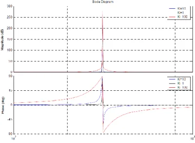
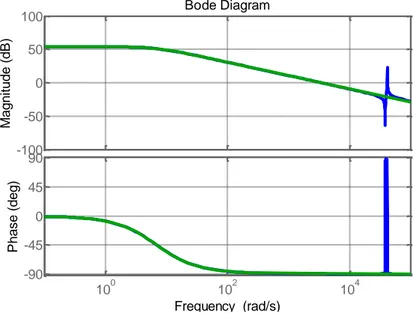
In the figure 1.8 the effect of ki is shown through the bode plot of CPres for kp=1, ω=2π50rad/s and ki=1, 10 and 100 rad/s. As it is possible to note, CPres behaves as a band-pass filter centered at the resonance frequency that it is equal to the grid frequency and ki determines the bandwidth centered at the resonance frequency where the attenuation is positive. Hence ki is usually tuned in order to obtain sufficient attenuation of the tracking error in case of grid frequency changes [1].
Fig 1.8 Bode plot of CPres with ki=1, 10,100 rad/s
Considering the P+Resonant controller and applying the final value theorem, the equation (1.14) is obtained:
25 Chapter 1 Photovoltaic Inverter
2 2 2 2 2 2 0 0.5 1 lim 0 0.5 1 s P I P k s Ts s Ls R s Ts k s k s k (1.14)Hence, it can be proven that, with e(s)=0, Δi(t) converges to zero when t → ∞ . The GI achieves an infinite gain at the resonant frequency, so the current reference tracking is ensured setting the resonant frequency of the controller to the fundamental frequency [11-13].
The P+Resonant controller will be used in the chapter 3 to analyze a critical scenario for the stability of the electric grid with a constant power load (CPL).
1.7 Maximum Power Point Tracking techniques
The maximum power point tracking (MPPT) control can be achieved with a number of different techniques, each one differing from the other for complexity, robustness, static and dynamic performance. To compare the different techniques it is possible to use the efficiency that can be defined as “the ratio between the energy extracted from the output terminals of a photovoltaic field and the energy really available” [14]. The available power depends on the solar irradiation while the extracted power depends on the impedance matching between source and load.
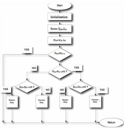
The Perturb and Observe (P&O) is the most widespread technique thanks to its simplicity and cost-effectiveness and also ABB Solar
Group usually implements this technique in its converters. It
implements a fixed-step hill climbing technique and, in the basic version, a fixed-amplitude perturbation of the duty-cycle (ΔD) is introduced by the controller at a fixed time step Ta. Varying the
converter duty cycle the system operation point changes and consequently the output power extracted by the photovoltaic source. In order to calculate the actual output power P[kTa], it is necessary to
measure the voltage and the current of the panel. This power is compared to the value obtained from the last measurement P[(k-1)Ta].
If (P[kTa]-P[(k-1)Ta]) is positive, the controller keeps changing the
26 Chapter 1 Photovoltaic Inverter negative the duty cycle change is reversed. The control algorithm can be summarized by the following equation [15]:
(k 1)Ta kTa ( kTa (k 1)Ta) ( kTa (k 1)Ta)
D D D D sign P P (1.15)
With this algorithm, once reached the maximum power point, the system operating point will swing around it. This causes a power loss that depends on the perturbation amplitude ΔD. If ΔD is large, the MPPT algorithm responds faster to sudden changes in operating conditions, with the trade-off of increasing the losses under stable or slowly changing conditions. If ΔD is small, the losses under stable or slowly changing conditions are reduced but the system has a slower response to rapid changes in temperature or irradiance level [14]. The P&O algorithm is explained by the flowchart in the figure 1.9.
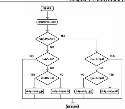
27 Chapter 1 Photovoltaic Inverter Another very used technique, the Incremental Conductance (IC) MPPT algorithm is based on the fact that the derivative of the output power (P) respect to the panel voltage (V) is equal to zero at the maximum power point. This derivative is greater than zero on the left of the MPP and lower than zero on the right of the MPP:
0 dP dV for
V
V
MPP (1.16) 0 dP dV forV
V
MPP (1.17) 0 dP dV forV
V
MPP (1.18)Since P=VI, where I is the panel current:
( )
dP d VI dV dI dI
I V I V
dV dV dV dV dV
(1.19)
From the equations (1.16) and (1.19):
-dI I dV V
(1.20)
Where dI/dV is the incremental conductance and I/V is the instantaneous conductance. This algorithm changes the system operating point, step by step, until the instantaneous conductance and the incremental conductance are approximately equal. In this operating point, the photovoltaic system reaches the maximum output power. Also in this case, as in the P&O algorithm, the key features are the amplitude and frequency of the perturbation [14]. A flowchart of this algorithm is depicted in the figure 1.10.
28 Chapter 1 Photovoltaic Inverter
Fig. 1.10 Incremental conductance algorithm flowchart
The advantage of the IC technique, respect to the P&O, is that the difference between the incremental conductance and the instantaneous conductance gives a direct knowledge of the distance between the operating point and the maximum power point. Therefore, exploiting this property, an amplitude variation of the perturbation can be realized, so that the controller uses a large perturbation step when the operating point is far from the MPP and reduces the perturbation amplitude to a minimum value once MPP is reached. In this way the algorithm is much more efficient in comparison to a classic IC algorithm. The disadvantages are the more complex computing compared to the P&O.
The industry interest is to use very cheap computer and, so, an adaptive P&O technique with minimum computing effort will be implemented in the chapter 4.
29 Chapter 1 Photovoltaic Inverter
References
[1] Teodorescu R., Liserre M., Rodriguez P., “Grid Converters for Photovoltaic and Wind Power System”, IEEE Press, WILEY [2] Ned Mohan, Tore M. Undeland, William P. Robbins “Power
Electronics: Converters, Applications, and Design,” Wiley&Sons INC.
[3] Editor in Chief Muhammad H. Rashid “Power Electronics Handbook” Academic Press
[4] Nabae, A.; Takahashi, I.; Akagi, H., "A New Neutral-Point-Clamped PWM Inverter," IEEE Transactions on Industry Applications, vol. IA-17, no.5, pp.518,523, Sept. 1981
[5] S. Buso, P. Mattarelli, “Digital Control in Power Electronics”, Morgan&Claypool Publishers
[6] K. Zhou, Kay-Soon Low, D. Wang, Fang-Lin Luo, B. Zhang, Y.Wang, “Zero-Phase Odd-Harmonic Repetitive Controller for a Single-Phase PWM Inverter”, IEEE Transactions on Power Electronics, vol. 21, no. 1, Jan. 2006, pp.193-201.
[7] R. Zhang, M. Cardinal, P. Szczesny, Dame, "A grid simulator with control of single-phase power converters in D-Q rotating frame," 33rd Annual IEEE Power Electronics Specialists Conference, 2002, vol.3, pp. 1431-1436.
[8] B.A. Francis and W.M. Wonham, “The Internal Model Principle for Linear Multivariable Regulators”, Appl. Math. Opt., 1975, pp.107-194.
[9] R.W. Erickson, D. Maksimovic, “Fundamentals of Power Electronics”, Second Edition, Springer-Verlag.
[10] W. S. Levine, “The Control Handbook: Control System Fundamentals”, Second Edition, CRC Press
30 Chapter 1 Photovoltaic Inverter [11] R. Teodorescu, F. Blaabjerg, U. Borup, M. Liserre, “A New
Control for Grid-Connected LCL PV Inverters with Zero Steady-State Error and Selective Harmonic Compensation”, Proc. of Applied Power Electronics Conference and Exposition, APEC 2004, vol. 1, pp. 580-586.
[12] D. N. Zmood, D.G. Holmes, “Stationary frame current regulation of PWM inverters with zero steady-state error”, IEEE Transactions on Power Electronics, vol. 18, no. 3, May 2003, pp.814-822.
[13] Y. Sato, T. Ishizuka, K. Nezu, T. Kataoka, “A New Control Strategy For Voltage-Type PWM Rectifiers To Realize Zero Steady-State Control Error in Input Current”, IEEE Transactions on Industry Applications, vol. 34, no. 3, May/June 1998, pp. 480-486.
[14] N. Femia, G. Petrone, G. Spagnuolo, M. Vitelli, Power Electronics and Control Techniques for Maximum Energy Harvesting in Photovoltaic Systems, CRC press, 2012.
[15] N. Femia, G. Petrone, G. Spagnuolo, M. Vitelli, “Optimization of Perturb and Observe Maximum Power Point Tracking Method”, IEEE Transactions on Power Electronics, vol. 20, no. 4, pp. 963-973, July 2005
Chapter 2
An improved Dead-Beat control based
on an Observe&Perturb algorithm
For photovoltaic applications, high power three-phase inverters have been adopted due to the less number of devices and its lower cost. Moreover, there are very cheap computers able to manage complex tasks and, so, the solutions with the centralized inverters have become more attractive.
The multi-level topologies are usually the best choice to comply, more easily, with the regulation requirements in terms of current quality injected into the grid. Indeed, the dc input voltage is divided in several levels bringing the output voltage to have fewer harmonics and being more similar to a sinusoidal waveform. This kind of converters needs to have the voltage clamped in order to avoid the voltage unbalance between the different levels [1], [2].
The most important topologies are diode-clamped inverter, i.e. Neutral-Point Clamped (NPC), capacitor-clamped, i.e. Flying Capacitor (FC) and cascaded-inverters (CI) with separate dc source [3]. The first NPC inverter, a passive NPC [2], has unequal loss distribution among the semiconductor devices with the result that the temperature distribution of the semiconductor junction is asymmetrical. To solve this problem, an active NPC inverter has been developed [4]. A NPC-based inverter, the AURORA ULTRA of 1.4MW, is developed by ABB Solar Group mainly for the Asian market.
The design of a NPC inverter presents several issues. Besides the problems of efficiency optimization and of switches stress reduction, the system needs to be connected and synchronized to the grid. For poor quality grids, as the ones encountered in Asia, ABB Solar Group noticed that this time can be very long, also 33% of the total system development time. A time so long is necessary since the system must be adapted to the real grid conditions that can be totally different compared to the ideal ones. Great changes of frequency and root-means square value can happen and also the system must be able to
32 Chapter 2 An improved DB control based on an O&P algorithm
ensure the respect of the regulation requirements during the grid faults. Hence the setup of this inverter, mostly a fine tuning of the control parameters, is often done on the installation site because the grid has not only no ideal behavior but also local unpredictably characteristics that have to be take into account for the correct operation of the inverter.
Those considerations point out the need to explore new control techniques that allow having better performance both static and dynamic. The current control techniques, as described in the chapter 1, can be divided in two main categories: linear as the Proportional-Integral (PI) and the State Feedback Controller and non-linear as the hysteresis and the predictive with on line optimization [5].
A technique to be actually used by the industry must be well-known and reliable and, so, the most widely used is the PI technique also by ABB Solar Group for its converters. But in literature, there are a lot of works that analyzed different techniques like the Dead-Beat (DB) control and the sliding-mode (SM) control. The SM control has been implemented with stability proof and tested, where the SM control regulates the currents to suppress its harmonics getting a low THD and ensure desired amplitude and phase shift while keeping a good grid synchronization [6], [7]. The DB control is very attractive for its intrinsic excellent dynamic response [8-11] but a reliable and simple implementation has not been found yet. Hence, the focus of this chapter is a comparison between the widely used PI and the DB controls. Different implementation structures like dq and αβ frames [12-14] can be used but as the focus is the two mentioned techniques the dq frame is selected. The modulation techniques for the NPC inverters are: multicarrier Pulse Width Modulation (PWM), Space Vector Modulation (SVM) and Selective Harmonic Elimination (SHE) [15], [16]. The multicarrier PWM is the most used for its simplicity of implementation. This technique can be divided in: Phase Disposition (PD), Phase Opposition Disposition (POD) and Alternative Phase Opposition Disposition (APOD) depending on how the carrier signals are taken [17], [18]. In this chapter, the PD PWM is selected because it has the lower THD [14] and the Neutral Point is balanced exploiting the modulation technique proprieties [19-22]. Hence, an improved DB control, based on a variation of the MPPT Pertrub&Observe algorithm [23] described in the chapter 1 and for that called Observe& Perturb (O&P), is develop providing the general
33 Chapter 2 An improved DB control based on an O&P algorithm
guideline to select its parameters. Also a comprehensive comparison between the PI, the standard DB, a hybrid solution between the PI and DB called Integral+DB (I+DB) and the proposed O&P DB control is performed for passive NPC inverters with a dedicated simulation tool, written in C++ language, since the existing commercial software, such as Simulink®, PSIM® and PSPICE®, allow to make the analysis only a specific level: system, circuit or device. Both O&P method and simulation tool are not only for NPC inverters but they are very general being able to be applied to all the converters.
It worth be noted that for very high power systems, even if it is possible to emulate their dynamic in a scaled version system, the companies like ABB Solar Group usually prefer to test all the solutions in the final real system to be sure of the inverter behavior as the grid is already unpredictable. For this reason, in this chapter, the simulation results are presented and the proposed O&P DB control is implemented on a TMS320F28379D Dual-Core Delfino™ Microcontroller (µc) to test the feasibility of all its components in a single embedded system. The choice of the F28379D µc is carried out to use the same family, the TI C2000, that ABB Solar Group implements on its converters and to have the best performance with a dual-core system.
2.1 Description of the simulator tool
The development of a simulation tool for a generic switching circuit has to take into account two aspects: to find the fundamental circuit equations and to detect the state of the switching devices.
In the implemented tool, exploiting the Chua-Lin algorithm [24], the normal tree and cotree are found and, then, the fundamental cutsets matrix is calculated in order to find the state model of the circuit. All the switches are model with a Piece-Wise Linear (PWL) Resistor with a great resistance value when the device is OFF and a very small resistance value when it is ON.
Hence, the software reads the topological information and the value of the single components by a text file and calculates the fundamental cutsets whose general expression is reported in the equations (2.1) and (2.2), where Fxx are the circuit topological
34 Chapter 2 An improved DB control based on an O&P algorithm
matrices and the symbols t and l denote that the component belongs to the tree and cotree respectively.
T T t t t l l l t t t l l l E C R L R C E C R L R C ii i i i i i vv v v v v v (2.1) 11 12 13 14 21 22 23 24 31 32 33 34 41 42 1 0 0 0 0 1 0 0 0 0 0 1 0 0 0 0 1 0 0 T T T L L L L T E T C T R T L E C R J L R C F F F F F F F F i F F F F F F (2.2)
From the topological matrices, it is possible to find the circuit state model in a very simple way. Indeed, as shown by the equations (2.3)-(2.6), the state and the input matrices are calculated through only matrix operations. 1 1 (0) (0) (0) (0) ( ) ( ) ( ) dx t Ax t Bu t A M A B M B dt (2.3) (0) 24 24 42 42 42 42 0 0 t T L t t LL TL LT LL C F C F M L F L L F F L F (2.4) 1 1 (0) 32 23 22 23 33 32 1 1 22 32 33 23 32 32 t t T t t t t L F R F F F R F R F A F F G F G F F G F (2.5) 1 1 (0) 32 13 21 23 33 31 1 1 12 32 33 13 32 31 t t T t t t t L F R F F F R F R F B F F G F G F F G F (2.6)
35 Chapter 2 An improved DB control based on an O&P algorithm
The state of the controlled switching devices (MOSFET, IGBT, etc.) is defined by the controller and by the modulator but it is necessary to detect the state of all synchronous devices (DIODE). These states are known for the specific application but, both to keep the software as more general as possible and both to analyze the circuit in any type of unpredictable conditions (grid and devices faults), the tool detects the synchronous switches state and checks the effective commutation of the controlled switches with an automatic and efficient method without a complete analysis of the circuit, exploiting the Compensation Theorem [25]. A commutation of the controlled devices imposed by the controller, with a PWL model, implies a change of resistance value in the switch branches and, so, a current variation in all branches of synchronous switches. If this variation is coherent with the previous state there is no commutation, otherwise there is and, hence, a new switch configuration can be analyzed in the same way. Thus, a consistent state of switching devices is found with a maximum of 3 steps, without calculating the state model for any configuration and then checking if it is coherent [25].
2.2 Standard controller design
The figure 2.1 shows the analyzed system. As can be seen, it is a three-level Neutral Point Diode Clamped Inverter described in the chapter 1. The PV source can be connected to the NPC input directly or, if it is necessary to adapt the PV voltage to the NPC input voltage, by means a further conversion stage. It worth be noted that, for grid connected inverters, the inductor Lg is usually not added as the grid
impedance is present. The problem is that this impedance is unknown as it changes with the connection point to the grid. To take into account this case, the inductor Lg is not considered in the control
techniques.
There are a lot of methodologies to control the output inverter phase currents Ia, Ib and Ic. The most intuitive is to use a controller for
each phase current but it is possible to exploit the symmetrical proprieties of the three-phase systems in order to reduce the number of controllers from three to two as described in the chapter and so the control is performed exploiting the Park Transform in the dq frame.
36 Chapter 2 An improved DB control based on an O&P algorithm
Fig 2.1 Neutral Point Clamped Inverter
The figure 2.2 shows the block diagram structure of this control.
abc -> dq Ia Ib Ic Id Iq Idref Iqref Controller Controller -ω(Lf+Lg) ω(Lf+Lg) + -+ -+ + Vdg + + + Vqg + Modulator PLL Vag Vbg Vcg Θ Θ abc -> dq Vag Vbg Vcg Vdg Vqg Θ Vd Vq
Fig 2.2 dq frame block diagram general structure
The Phase Disposition Carried-Based (PD-CB) PWM technique is adopted for this circuit since it has been demonstrated in literature that it leads to less harmonic distortion [14]. This technique is based on the comparison between the modulator signals, one for each inverter leg, and two triangular carried signals that are in phase. The modulation signals are achieved by an anti-transformation of the output control signals Vd and Vq in the abc frame. Also the neutral point (NP)
balancing has been implemented through a DC link compensation added into the modulation as it is very similar to the balancing used by
37 Chapter 2 An improved DB control based on an O&P algorithm
active NP voltage control techniques [20]. The figure 2.3 shows the block representation of the implemented modulation technique.
V*a,b,c
÷
+ -1/(Vdc/ 2) V_Cdc_up÷
+ -1/(Vdc/ 2) V_Cdc_down 1 0 -1 0 Sa,b,c1 Sa,b,c2 Sa,b,c3 Sa,b,c4 dq -> abc V*a V*b V*c Θ Vd VqFig 2.3 Phase Disposition Carried-Based Pulse Width Modulation
The circuit parameters, reported in the table 2.1, are based on the
AURORA ULTRA inverter of ABB Solar Group and will be used for
the controllers design and simulations of the next sections.
Vdc 700 V R_Lf 1 mΩ Cdc 1 mF R_Cf 1 mΩ Cf 45 µF R_Lg 1 mΩ Lf 250 µH Ron_switch 1 mΩ Lg 45 µH Roff_switch 100 kΩ Rdc 1 mΩ fswitching 20 kHz R_Cdc 1 mΩ fgrid 50 Hz Vg_rms 186 V
38 Chapter 2 An improved DB control based on an O&P algorithm
2.2.1 Proportional-Integral Linear Control design
The classical PI control loop with grid voltage feedforward is shown in the figure 2.4, where GPI(s) is the transfer function of the PI
controller and Gf(s) is the transfer function of the filter (the plant).
Iref_d,q+-
G
PI(s)
-+ Vg_d,qG
f(s)
I_d,qFig. 2.4 PI current control loop
The effect of the capacitor Cf is neglected in the filter transfer
function since the filter frequency response i/v with and without the capacitor is the same at the interest frequencies, as shown in the figure 2.5 with the values of the table 2.1. Hence, it is possible to define LT=Lg+Lf and RLT=R_Lg+R_Lf. -100 -50 0 50 100 M a g n it u d e ( d B ) 100 102 104 -90 -45 0 45 90 P h a se ( d e g ) Bode Diagram Frequency (rad/s)
Fig 2.5 Filter frequency response i/v with (blue line) and without (green line) capacitor
39 Chapter 2 An improved DB control based on an O&P algorithm
The equations (2.7) and (2.8) show the transfer functions GPI(s) and
Gf(s).
1
( )
f T TG s
R
sL
(2.7)( )
I PI Pk
G
s
k
s
(2.8)To calculate kP and kI, a cross-over frequency fc equal to 700Hz and a
phase margin ϕm equal to 70° have been imposed to the open-loop
gain transfer function Gf(s)GPI(s), with the values of the table 2.1,
leading to the following values:
1.2 2000 P I k k rad s (2.9)
Typically, a digital device, such as a microcontroller or a DSP, is used to implement this controller [26]. Hence, the transfer function GPI(s) is discretized with the Tustin transform as shown in the
equations (2.10): 2 1 1 1 ( ) ( ) 2 1 ( ) (( 1) ) ( ) (( 1) ) 2 ( ) ( ) ( ) z s I Tc z PI P PI P I I I I P I k Tc z G s k G z k k s z e kTc e k Tc u kTc k Tc u k Tc V kTc k e kTc u kTc (2.10)
where e(kTc) = iref - i(kTc) is the tracking error at the instant kTc.
The sampling frequency has been chosen to 20kHz, typical value used for this inverter by ABB Solar Group.
Also, coupled terms between the components d and q are also present with the Park Transform, as shown in the chapter 1, equation (1.5) and so decoupled compensation terms are added in the control laws [14], [26], as shown in the figure 2.2.
40 Chapter 2 An improved DB control based on an O&P algorithm
Thus, taking into account the feedforward grid voltage compensation and the decoupling term of the Park Transform, the following control laws are implemented:
( ) (( 1) ) ( ) (( 1) ) 2 ( ) ( ) ( ) ( ) ( ) (( 1) ) ( ) (( 1) ) 2 ( ) ( ) ( ) ( ) d d dI I dI d P d dI dg T q q q qI I qI q P q qI qg T d e kTc e k Tc u kTc k Tc u k Tc V kTc k e kTc u kTc V wL i kTc e kTc e k Tc u kTc k Tc u k Tc V kTc k e kTc u kTc V wL i kTc (2.11)
2.2.2 Dead-Beat control design
The design of the DB control is carried out on the basis of the grid filter mathematical model [14], [26] in term of dq transformation where, as for the PI control, the capacitors Cf are neglected.
Looking at the figure 2.1 and defining LT=Lg+Lf and
RLT=R_Lg+R_Lf, it is possible to write [26]: 1 0 0 2 1 1 1 0 0 1 1 0 1 0 1 2 1 0 1 0 3 0 0 1 1 1 2 0 0 1 ag a a a LT b b b bg T T T c c c cg V I I V R d I I V V dt L L L I I V V (2.12) Considering the Park Transform of the system equations (2.12):
1 1 0 0 1 1 0 0 LT gd d T d T d T q LT q q gq T T T R w V i L i L V L d i R i V V dt w L L L (2.13)