A
LMA
M
ATER
S
TUDIORUM
·
U
NIVERSITÀ DI
B
OLOGNA
Scuola di Scienze
Dipartimento di Fisica e Astronomia Corso di Laurea Magistrale in Fisica
NOVEL ORGANIC SEMICONDUCTING
SMALL MOLECULES FOR X-RAY
DETECTION
Relatore:
Presentata da:
Prof.ssa Beatrice Fraboni
Tommaso Neri
Correlatore:
Dott.ssa Laura Basiricò
i
Abstract
L’elettronica organica ha trovato negli anni recenti diverse applicazioni, anche in dispositivi di uso quotidiano, come ad esempio gli schermi OLED (Organic Light Emitting Diode). I semiconduttori organici possono essere depositati con tecniche a basso costo, anche su scala industriale, e su grandi aree, fattore, quest’ultimo, che li rende particolarmente adatti alla fabbricazione di sensori di radiazioni ionizzanti. Il lavoro presentato riguarda la realizzazione di transistor organici a film sottile e la loro caratterizzazione, come transistor e come sensori di raggi X. In particolare, l’obiettivo di questo progetto sperimentale è il confronto delle sensibilità di due tipi di dispositivi
fabbricati da soluzioni delle molecole diF-TES-ADT
(5,11-bis(triethylsilylethynyl)anthradithiophene) e diF-TEG-ADT
(5,11-bis(triethylgermylethynyl)anthradithiophene), appartenenti alla classe degli eteroaceni sostituiti. Nella prima molecola sono presenti due gruppi funzionali identici in cui è contenuto un atomo di silicio, mentre nell’altra essi contengono un atomo di germanio, caratterizzato da un numero atomico più alto. In questo lavoro viene dimostrato che il numero atomico più alto, grazie al maggiore coefficiente di assorbimento per la radiazione X, comporta una sensibilità più alta per il sensore di razioni ionizzanti, come confermato dai risultati ottenuti.
ii
Abstract
In recent years Organic electronics has known a good development, and nowadays the organic semiconductors are employed in several applications, even in everyday-use devices, like the OLED (Organic Light Emitting Diode) screens. Organic devices can be realized by depositing the organic semiconductors by low cost techniques easily extendable to the industrial scale. Moreover, the possibility to realize the deposition over large areas makes them particularly suitable for the fabrication of ionizing radiation detectors. In this experimental work two types of thin film organic transistors were fabricated with solutions of two molecules, and then they were characterized electrically as transistors and as X-ray detectors. The motivation of this thesis is the comparison of the sensitivities of two types of devices, realized respectively with solutions of diF-TES-ADT bis(triethylsilylethynyl)anthradithiophene) and diF-TEG-diF-TES-ADT (5,11-bis(triethylgermylethynyl)anthradithiophene) molecules, belonging to the class of substituted heteroacenes. In the structure of the first molecule there are two identical functional groups containing a silicon atom, whereas in the second one these functional groups have a germanium atom, characterized by a higher atomic number. In the thesis we demonstrate that the higher atomic number, thanks to its higher X-ray absorption cross section, leads to a higher sensor sensitivity, as confirmed by the results obtained.
iii
Contents
Introduction ... 1
1. Organic Electronics ... 3
1.1. Charge carrier transport in organic semiconductors ... 6
1.1.1.Mobility and dependence on temperature ... 7
1.1.2.Mobility and dependence on electric field ... 7
1.1.3.Charge injection into organic semiconductors ... 9
1.2. Organic field effect transistors ... 11
1.2.1.Organic small molecule for OFETs: soluble acenes and heteroacenes ... 14
2. Ionizing radiation detection ... 23
2.1. Ionizing radiation interaction with matter ... 24
2.1.1.Photoelectric absorption... 24
2.1.2.Compton scattering ... 25
2.1.3.Pair Production... 26
2.2. Simplified detector model ... 27
2.3. Detection of X-rays and γ-rays ... 29
2.4. Organic direct ionizing radiation detectors ... 31
2.4.1.Organic Direct Detectors based on Thin Films ... 31
2.4.2.Organic direct detectors based on Organic Semiconducting Single Cristal (OSSC) ... 42
2.5. Detector based on alternative materials: perovskites ... 48
2.6. Hybrid organic/inorganic ionizing radiation detectors ... 50
3. Materials and methods ... 56
3.1. Devices preparation... 57
3.1.1.Fabrication of drop-casted samples ... 58
3.1.2.Fabrication of spin-coated samples ... 59
3.2. Electrical characterization ... 59
3.3. X-Ray photoresponse characterization ... 62
3.4. Data Analysis ... 68
iv
4.1 Devices realized by drop-casting from solutions at wt.0.5% ... 73
4.2 Devices realized by spin-coating from solutions at wt.1.2% ... 79
4.3 Devices realized by spin-coating from solutions at wt.0.5% ... 86
4.4 Devices realized by spin-coating from solutions at wt.2% ... 94
Conclusions ... 100
Appendix ... 103
A.1 Leakage current plots and raw data plots ... 103
A.1.1Devices realized by drop-casting from a solution of diF-TES-ADT at wt.0.5% ... 104
A.1.2Devices realized by drop-casting from a solution of diF-TEG-ADT at wt.0.5% ... 105
A.1.3Devices realized by spin-coating from a solution of diF-TES-ADT at wt.1.2% ... 106
A.1.4Devices realized by spin-coating from a solution of diF-TEG-ADT at wt.1.2% ... 107
A.1.5Devices realized by spin-coating from a solution of diF-TES-ADT at wt.0.5% ... 108
A.1.6Devices realized by spin-coating from a solution of diF-TEG-ADT at wt.wt.0.5% ... 109
A.1.7 Devices realized by spin-coating from a solution of diF-TES-ADT at wt.2% ... 110
A.1.8Devices realized by spin-coating from a solution of diF-TEG-ADT at wt.2% ... 111
1
Introduction
In the last years the Organic electronics has known a wide development. Until the first uses of the organic semiconductors, about 40 years ago, only their inorganic counterpart, mainly silicon and germanium, was employed in the realization of electronic devices. The main disadvantage of traditional inorganic materials consists in their fabrication, characterized by high energetic and economic costs. On the contrary, the most common organic semiconductors are soluble in organic solvents (often they are functionalized in order to obtain this solubility), and for this reason they can be deposited over the respective substrates by means of low-cost deposition technique realizable in a standard laboratory, and extendable to the industrial scale. Starting from 2007 the organic semiconductors have been proposed as direct X-ray detectors [1], however they are less stable over the time than the inorganic materials and not always reach high sensitivities, because of the low atomic number, and consequently low absorption cross section which characterizes them. In order to enhance the sensitivity, in the literature it is possible to find some solutions, like the addition in the active layer of the devices of nanoparticles with a high atomic number [2] [3], or the improvement of the conductivity, for example adding single walled carbon nanotubes, that provide a better mobility for holes [4]. The purpose of the experimental work carried out during this thesis is the comparison of the X-ray detection performance of two types of organic thin film transistors realized starting from solutions of two organic small molecules, diF-TES-ADT (5,11-bis(triethylsilylethynyl)anthradithiophene) and diF-TEG-ADT (5,11-bis(triethylgermylethynyl)anthradithiophene), belonging to the class of the substituted heteroacenes. In the structure of diF-TES-ADT there are two identical functional groups containing a silicon atom and in the structure of diF-TEG-ADT the same functional group contains a germanium atom. The germanium atom has a higher atomic number Z in comparison with silicon, for this reason a higher sensitivity should be expected for the device realized with diF-TEG-ADT. Within this work several devices were realized starting from solutions in chlorobenzene of the two molecules at three concentrations in weight (wt.0.5%. wt.1.2%, wt.2%). The solutions at wt.0.5% were deposited by means
2
of two deposition technique, drop-casting and spin-coating, whereas the other ones were deposited only by spin-coating. The best performance as X-ray detector and the highest sensitivity were obtained with the devices realized from a solution of diF-TEG-ADT at wt.1.2% deposited by spin-coating.
In this thesis, the first chapter describes the properties of organic semiconducting materials, starting from their fundamental constituent: the carbon atom. Next, a description of the electrical behaviour of the organic semiconductor is reported and subsequently a paragraph is dedicated to the Organic Field Effect Transistors (OFETs), focusing on the organic small molecules most used for such application. The chapter finishes with an overview of the results reported in the literature in this field. The second chapter reports a description of the X-ray detectors, at first in general, and subsequently with a focus over the organic detectors. Finally, it reports a description of the results reported in the literature about the X-ray detectors realized with organic materials or hybrid organic/inorganic materials. In chapter 3 the experimental setups, the procedure of realization of the devices and the characterization carried out are presented. The subsequent chapter 4 illustrates the results obtained during this work.
3
1.
Organic Electronics
Organic semiconducting materials are carbon-based materials. Its fundamental constituents, in addition to carbon, are hydrogen and other elements like oxygen, nitrogen, halogens, etc. The ground state of atomic carbon is formed by six electrons, two in 1s orbital, two in 2s orbital, and two in two of three 2px, 2py, and 2pz orbitals [5].
The wave-like behaviour of an electron may be described, according to quantum mechanics, by a complex wave function depending on position and time ψ(r,t). The square modulus of this wave function, |ψ(r,t)|2, is equal to a probability density, and its integral over a certain volume V gives the probability of finding the electron in that volume at the instant of time t. The region of the space in which this probability is at least the 90% is called atomic orbital and its shape depends on how the wave function is mathematically defined. Each orbital has a maximum of two electrons and it is characterized by a different set of quantum numbers [6].
In configuration 1s22s22px12py1carbon can make only two covalent bonds, but when one
of the 2s electrons move into the empty 2pz orbital it makes four covalent bonds. In this
case, new hybrid orbitals are formed from a linear combination of the 2s-orbital with the orbitals, that is named hybridization. When all 4 orbitals (one 2s and three 2p-orbitals) are involved in the hybridization, the resulting four equivalent orbitals, named sp3 orbitals, point into the 4 corners of a tetrahedron with an angle of 109,5° between
them (Figure 1.1) [5].
Figure 1.1: (a) Atomic carbon: the four sp3 orbitals are directed toward the corners of a tetrahedron. (b) The orbital structure of methane shows the overlap of the four sp3 orbitals of carbon with the s orbitals of four hydrogen atoms. Four σ (covalent) bonds between carbon and hydrogen are formed [7].
4
In more detail, hybridization is a mathematical process of linear combination of atomic orbitals of different type and similar energy within the same atom, that allows to achieve new hybridized isoenergetic orbital [8], more suitable for the description of molecule structure [9]. The number of bonds that a carbon atom makes is determined by the number of hybrid orbitals and remaining p-orbitals. In a chemical bond the electrons have equal probability to orbit around the first atom or around the second, so they cannot be assigned to atomic orbitals, but is necessary to associate them with molecular orbitals, that are approximated as linear combination of atomic orbitals [5]. The bonds formed by s-orbitals or their hybrids and p-orbitals are called σ-bonds and the correspondents electrons are called σ-electrons [7].
Figure 1.2: (a) σ-bond and π-bond [7]. (b) Aromatic ring: delocalization of π orbitals [10].
When one 2s-orbital combines with two of the three 2p-orbitals, three hybrid sp2-orbitals lying on the same plane are formed. The unhybridized orbital (2pz), on the contrary, is
standing perpendicular to them [7]. If two sp2orbitals, belonging to two different sp2
hybridized carbon atoms overlap, give rise to the so called σ-bond. When this bond is forming, also the unhybridized pz orbitals start to interacting, and, as a results, they form
the bond named π-bond (Figure 1.2a) [7]. σ-bonds are very strong, and the respective electrons are not free to move, because are too localized, thus they do not contribute to the charge transport mechanism. Therefore, σ-bonds form the skeleton of the structure, and moreover, are responsible for the geometrical properties of the resulting molecule. On the contrary, π-bonds are very weak and π-electrons are delocalized so they can freely move across the molecule, especially in presence of an electric field [7].
A class of molecule used in organic electronic is the one of the conducting polymers, the whose key structure is a linear chain of conjugated units with alternate single and double bonds. In these macromolecules, the p-orbitals of the π-electrons overlap,
5
producing a reconfiguration of the arrangement of the electrons, that concerns the energy levels [7]. Another class of organic molecules used are the aromatic molecules, in which hybridized atom orbitals of carbon atoms are bounded by σ-bonds or π-bonds. σ-bonds are strong connection parallel to the molecular plane, whereas π-bonds are delocalized bonds that form molecular orbitals (Figure 1.2b) [10].
It is possible to separate the molecular energy levels into two categories: π and π* bonding and anti-bonding respectively, which form a band-like structure (Figure 1.3). The occupied π-levels are equivalent to the valence band of inorganic semiconductors, whereas unoccupied π*-levels are equivalent to the conduction band [7]. Two orbitals are very important: HOMO (Highest Occupied Molecular Orbital) and LUMO (Lowest Unoccupied Molecular Orbital). HOMO is the outer orbital occupied by electrons, and LUMO is the first unoccupied energy level [10].
Figure 1.3: π-bonding and π*anti-bonding molecular orbitals
[7].
The band gap given by the difference between energies of HOMO and LUMO for polymers is given by the equation (1.1) [7]:
EG=ELUMO-EHOMO= (N+1)2h2 8me(Nd)2≈ h2 8med2N for large N (1.1)
6
Where h is the Planck Constant, me the electron mass, N the number of atoms of
polymeric chain and d the distance between the atoms within the polymeric chain. In an aromatic molecule, similarly to a polymeric chain, an increase of aromatic rings (a longer chain) is associated to a smaller energy gap between HOMO and LUMO [10].
1.1.
Charge carrier transport in organic
semiconductors
Several models have been developed to explain the charge transport in organic semiconductors, but a universal theory that can describe charge transport in organic materials does not exist and transport properties are not fully explained [7].
Inorganic semiconductors are characterized by very strong covalent bonds. In these materials charge carriers move as highly delocalized plane waves in wide bands and, usually, their mobility is very high. In this case the scattering of the carriers, mainly on phonons, thermally induced lattice deformations, limits the charge transport. In the organic semiconductors, on the contrary, the weak intermolecular interaction forces, usually van der Waals interactions, make the vibrational energy of the molecules similar to the intermolecular bond energy at or above room temperature, therefore the mean atomic distance can be bigger than mean free path of charge carriers, and consequently, transport occurs by hopping of charges between localized states; in this case charge transport is phonon assisted [7]. Organic disordered materials have a gaussian DOS, whereas their inorganic counterpart is characterized by an exponential DOS. In the former ones the relaxation process of excess charges, created for injection or photoexcitation at an arbitrary energy, occurs trough relaxation into lower-lying energy states in the band tail as time evolves. In this case, the energy of photoinjected charges will eventually reach a steady state value, named equilibration energy, ε∞. and the
excited charges will undergo energy relaxation, reaching eventually the equilibrium at the given time trel. After trel transport will be determined by thermal excitation from
7
1.1.1.
Mobility and dependence on temperature
Temperature plays an important role in the charge transport mechanism. In single crystals, where the charge transport is bandlike and impeded by scattering processes, the mobility decreases with temperature, with a power law behaviour described by the equation (1.2) [11]:
μ≈T-b (1.2)
b
∈
[1,-3] [6]On the contrary, in disordered materials, where conduction, instead of band transport, is due to hopping between localized states, which occurs with thermal activation that allows to overcome the energy barriers between localized states, the mobility increases strongly with the temperature (Arrhenius dependence) as described by the equation (1.3) [11]:
μArrhenius ≈ μ∞e- kTEa (1.3) Where µ∞ is a temperature independent prefactor and Ea>0 the activation energy.
The Gaussian disorder model (GDM) provides another parametrization (equation (1.4)) of the temperature dependence for mobility, obtained from the results of theoretical simulations for transport [11]:
μGDM ≈ μ∞e-(TT )0
2
(1.4)
Where T0 is related to the DOS width and gives an indication about the amount of energy
disorder.
1.1.2.
Mobility and dependence on electric field
When charge transport is due to hopping between localized states, the application of an electric field E⃗⃗ lowers the activation barrier (Figure 1.4) for charge transfer between two localized states with different energies εi andεj separated by a distance rij, of an amount
8
-qr ij∙E⃗⃗ , allowing to the charge carriers an easier access to shallower states. This fact,
moreover, modifies their energy distribution [11]. The modification of mobility by an electric field can be modelled using a Poole-Frenkel mechanism, that describes the lowering of the thermal excitation barrier for a charge in a localized state characterized by a coulombic potential. This model provides an equation like the (1.5) [11]:
μPF ∝eγPF√E (1.5)
Where γPF is the Poole-Frenkel temperature dependent factor.
Figure 1.4: Hopping of a charge
in presence of an electric field, that makes more states available to the charge. The shaded region represents the occupied states [11].
This ln(μ)~√E behaviour usually characterizes a conduction mechanism in which charge carriers must escape from charge trapping centers, but organic systems do not contain a sufficiently large number of this kind of traps, so Gartstein and Conwell [12] proposed, and showed, that for a wide range of electric fields, transport through a system in which the disorder is spatially correlated determines a Poole-Frenkel behaviour; fluctuations in the site energies caused by long-range interactions, as charge-dipole or dipole-dipole interactions with neighbouring molecules, can cause this correlation. Moreover, amorphous organic materials are characterized by a some degree of short
9
range order, therefore the resulting small correlations in position and conformation can increase the energetic correlation [11].
1.1.3.
Charge injection into organic semiconductors
In addition of charge transport along the organic semiconductor, physical properties of organic devices can be strongly influenced by the metal/organic semiconductor interfaces, that can modify the amount of charge carriers injected to the channel. [7].
Figure 1.5: Metal-semiconductor interface in a n-type semiconductor (a) and in a p-type
semiconductor (b) [5].
The metal inorganic semiconductor junction is called Schottky junction. In Figure 1.5a is explained the case of an ideal, neutral n-type semiconductor with valence band energy Ev and conduction band energy Ec, that is put into contact with a neutral metal of high
workfunction Φm (Φs<Φm, where Φs is the semiconductor workfunction). Before the
contact, the Fermi energy of n-type semiconductor is at an energy Δn below the conduction band edge, characterized by an electron affinity EA. When the contact from
metal and semiconductor is made, electrons start to diffuse from semiconductor into the metal and they finish to flush when thermal equilibrium is reached, and the Fermi levels lined up. As a result, metal has additional negative charge that is lacking in the
10
semiconductor; this negative excess charge at the metal surface implies the collection of an equal and opposite charge in the region of the semiconductor next to the interface to form a depletion layer. The Figure 1.5 show the potential drop bi in the
semiconductor layer adjacent to the interface, associated with a built-in field, consequently formed. At the interface, the work function of the metal, the semiconductor ionization potential (IE) and the electron affinity are unaltered with respect to the vacuum level [5]. A p-type-semiconductor metal Schottky junction has an analogous behaviour. In this case a Schottky barrier is formed when Φs>Φm (Figure
1.5b). When the semiconductor is organic the conduction and valence band are equivalent respectively to the LUMO and HOMO levels (Figure 1.6) [7].
Figure 1.6: Metal-organic semiconductor interface: energy diagram without dipole
barrier (a) and with a dipole barrier Δ (b). IE is the ionization energy, EA the electron affinity of the organic semiconductor, Φe the electron barrier, Φh the hole barriers, Evac(O) the organic semiconductor vacuum level and Evac(M) the metal vacuum level [13].
Gold has a relatively high work function (Φgold=5.1 eV), therefore it forms a low hole
injection barrier with the most organic semiconductor, and for this reason it is used for the realization of p-type organic transistors [7].
However, several factors can modify the Mott-Schottky type of band bending, like the formation of surface dipoles [7] and traps (mostly produced during contact fabrication) [14] at the interface between the metal and the organic semiconductor.
11
1.2.
Organic field effect transistors
The field effect transistor (FET) is a 3-terminal device used in several electrical circuits [15]. Organic transistors are characterized by a thin film or a single crystal made of an organic semiconductors as active layer [6]. The Organic Field Effect Transistors are in general named OFETs. When the active layer is constituted of a thin film the acronym OTFT (Organic Thin Film Transistors) is used. The organic transistor can be imagined as a plane capacitor where the gate electrode constitutes one plate and the organic semiconductor constitutes the other plate. Two other electrodes characterize the transistor: the source and the drain, that are directly in contact with the semiconductor. All these elements have a thickness largely lower than one micrometer, therefore the device is constructed on a thicker, insulating substrate, that does not contribute to the electrical behaviour of the device itself [16]. In Figure 1.7 the three more popular organic transistor geometries are depicted.
Figure 1.7: Organic-transistor geometries: bottom gate and bottom contacts (a), bottom gate and top
contacts (b), top gate and bottom contacts (c). S indicates the source electrode, D the drain electrode and G the gate electrode [16].
The interest for OFETs and organic electronics has increased over the past few years. These devices are intensively studied for many applications such as displays, smart tags and sensors, because organic semiconductor allow to produce low cost devices on plastic substrates, potentially flexible [17], and they can be deposited over large areas, opening thus a new market segment [7].
In the OFETs, applying a voltage VD between the source and drain, there is no intrinsic
conduction, but only a flow of charges injected from the electrodes, because the density of thermally induced charge carries is very low, especially in comparison with transistors realized with inorganic semiconductors [16].
12
If a gate voltage VG, larger than the given threshold VT, is applied, an equal amount of
charge, but opposite in sign to the gate voltage, appears at both sides of the dielectric, and the conducting channel is formed. [16]. The density of charge carriers is uniform all along the channel if no voltage is applied to the drain. When a voltage VD is applied to
the drain the potential at a generic point of the channel is modified by an amount -V(x), in a continuous way, from the source electrode (x=0, V(x)=0) to the drain electrode (x=L, V(x)=VD), as depicted in Figure 1.8. L is the channel length.
Figure 1.8: (a) Field-effect transistor and corresponding voltages. (b) Variation of the voltage along the
channel on dependence of drain voltage VD. (c) Variation of the charge in the conducting channel: when VD=0, the charge is uniform, while when VD=VG–VT, the charge drops to zero near the drain. When the drain voltage VD overcomes this value a depletion zone, that is a void of charge carriers, is formed. ΔL is the shortening of the channel. [16]
If, in addition to gate voltage VG larger than the threshold voltage VT, a small source
drain voltage VD (with VD<<-(VG-VT)) is applied, the gate induced field is still almost
uniformly distributed along the conducting channel. In this case the transistor is working in linear regime, and the current increases linearly in dependence on source drain voltage VD. If VD increases and becomes larger of VG-VT (that is VD≥(VG-VT)), the gate
field at the drain electrode is zero, and a depleted area with no induced free charge carriers is formed. This phenomenon is named pinch-off. When it is reached, the current flowing across the channel saturates, and an increase in the source drain voltage does not produce significant effects on the measured current. This regime is called saturation regime [7]. The saturation region and the linear region in an output characteristic are
13
depicted in Figure 1.9. The equations describing the OFET drain current ((1.6) for the linear regime and (1.7) for the saturation regime) are the following [11]:
(ID) lin= W L μCi(VG-VT -VD 2 ) VD (linear regime) (1.6) (ID) sat= W 2LμCi(VG-VT)2 (saturation regime) (1.7) Where W is the channel width, µ is the field-effect mobility of the semiconductor, L the channel length and Ci the capacitance per unit area of insulator layer.
Figure 1.9: Output characteristic of an OFET. Linear region and saturation
region are indicated [7].
Mobility, threshold voltage and Ion/Ioff ratio are three parameters required for estimating
the quality of an organic transistor [16]. Mobility and Threshold voltage extraction is possible rewriting equations (1.7), obtaining the equation (1.8):
√(ID)sat=√
W
2LCiμ(VG-VT) (1.8)
The plot of the square root of the saturation current against gate voltage would result in a straight line. Mobility is then obtained using the equation (1.8), knowing the slope of the straight line, whereas threshold voltage is given by the extrapolation of the line to zero current. However this method has the disadvantage that in the saturation regime the density of charge varies considerably along the conducting channel (it is maximum
14
near the source and practically zero at the drain, see Figure 1.8c) [16]. Moreover, the mobility in organic semiconductors depends on several parameters, among which the density of charge carriers, as a result the mobility in saturation regime is not constant along the channel, and the calculated value only represents a mean value [16].
1.2.1.
Organic small molecule for OFETs: soluble
acenes and heteroacenes
To date acenes are one of the most intensely investigated classes of organic semiconductors; for the fabrication of OFETs especially rubrene [18] and pentacene [19] are considered benchmark materials. The best performance registered for an organic transistor has been obtained with rubrene single crystals, that demonstrated a contact-free intrinsic mobility of 40 cm2/(Vs) [20] and a maximum transistor mobility of 18 cm2/(Vs) [20]. Moreover, single crystals allow to analyze more easily the effects of defects and impurities on the device characteristics, and to get measurements of intrinsic electrical properties [21]. On the contrary, the morphological and electrical properties of thin films are strongly related to the characteristics of the substrate on which they are deposited, making them not properly suitable for these analyses. Nonetheless, thin films are the most appropriatesystems for applications in large area organic electronics [16].
Nevertheless, acenes have the disadvantage of poor solubility, which significantly limits the application of solution-based deposition process for device realization [11], for this reason pentacene is substituted with trialkylslyl acetylene, yielding thus a soluble pentacene derivatives, that, moreover, allow to reach an improvement in stability. The functionalization process produces almost exclusively π-stacked materials, in which changes in crystal packing induced by the substitution of the silicon are useful in tuning materials for performance in transistors (planar electrode geometries) or in photovoltaic cells (stacked electrode geometry) [11]. In transistors, molecules with two-dimensional
15
stacking interactions, like TIPS-Pentacene
(6,13-Bis(triisopropylsilylethynyl)pentacene, Figure 1.10), perform better.
Figure 1.10: TIPS-Pentacene [11].
In small semiconducting molecules, charge transport is highly sensitive to intermolecular π-orbital overlap, and any its variations, for example induced by molecular packing, can result in variations in charge transport [22]. As already mentioned, in organic semiconductors, the dominant interactions are van der Waals and weak electrostatic (i.e. quadrupole) interactions. They are much weaker relative to ionic and covalent interactions and non-specific compared to hydrogen bonding, as a result polymorphism, defined as the ability for a compound to adopt multiple crystalline packing states, is predominant among organic molecules at near ambient conditions. Moreover, different polymorphs often have distinct physical properties such as the solubility, melting point, crystal habits, electronic, optical and mechanical properties, therefore it is important to control the polymorphism [22]. For example, in the case of TIPS-Pentacene, in thin film transistors realized by solution shearing, hole mobility was measured as 8.1 cm2/(Vs) in an nonequilibrium polymorph, whereas the equilibrium form was characterized by an hole average mobility of 5.8∙10-2 cm2/(Vs) [23]. A problem that may arise in the TIPS-Pentacene OTFTs is the hysteresis in the electrical characteristics. This phenomenon occurs because films formed of TIPS-Pentacene tend to consist of numerous small crystalline grains, and the boundaries between grains often fall within the channel of OTFTs devices, producing the hysteresis in the electrical characteristics. Its appearance is related to the width of the lath-shaped grains [24]: grains with width <4 µm exhibit pronounced hysteresis and low mobility (<0.01 cm2/(Vs)) whereas grains width >6 µm show minimal hysteresis and high mobility [11].
16
Another class of compound investigated for organic electronic applications are the
silylethine-substitued heteroacenes. TES-ADT
(5,11-Bis(triethylsilylethynyl)anthradithiophene) was the first molecule of this kind tested in device applications (Figure 1.11a). Nowadays TES-ADT exhibited a mobility of 1.1 cm2/(Vs) [25], measured in transistor configuration, realized by spin-coating.
Figure 1.11: (a) TES-ADT (b) diF-TES-ADT [11].
Spin-coating of these materials yields, as for TIPS-Pentacene, amorphous films with very poor mobility, but the weaker interactions between molecules make this compound highly suitable to annealing techniques [11]. In order to enhance the interaction between molecules in ADTs (anthradithiophenes), partially halogenated derivatives were synthesized and analysed. Especially the fluorine-substituted derivatives, like diF-TES-ADT (2,8-difluoro-5,11-bis(triethylsilylethynyl)anthradithiophene, Figure 1.11b), proved to be particularly interesting, typically undergo rapid crystallization during film formation thanks to the improved noncovalent interactions imported by fluorine atoms. also when the deposition is realized by spin-coating [11].
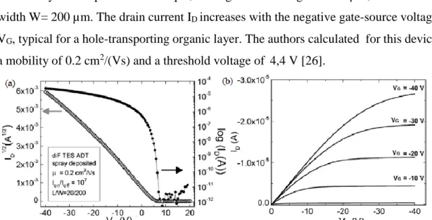
An example of the use of diF-TES-ADT in transistors fabrication is reported in the paper Azarova et al. [26], that describes devices fabricated by spray-deposition, a simple and inexpensive method, easily scalable from laboratory-based samples to large-area electronics, that was carried out at room-temperature. Moreover, spray-deposition is more efficient than spin-coating, where, unlike spray-coating, most solution is wasted during spinning [26]. In this deposition technique the organic semiconductor solution is aerosolized under high pressure argon, and the droplets are collected on the device structure, consisting of heavily doped Silicon wafer used as substrate and gate electrode, and thermally grown SiO2 layer as the gate oxide.
17
The source and drain contacts of this device are made of Ti/Au, deposited by e-beam evaporation. Figure 1.12 shows the current-voltage characteristics of a transistor realized by this deposition technique, having channel length L=20 µm, and channel width W= 200 µm. The drain current ID increases with the negative gate-source voltage
VG, typical for a hole-transporting organic layer. The authors calculated for this device
a mobility of 0.2 cm2/(Vs) and a threshold voltage of 4,4 V [26].
Figure 1.12: Electrical characteristics of a spray-deposited diF-TES ADT transistor presented in
Azarova et al. [26] (a) Current-voltage characteristics (log(ID) vs.VG) in the saturation regime (VD =-40 V). In the left axis is reported ID1/2.(b) Output characteristic. The dimensions of channel length (L) and channel width (W) are indicated [26].
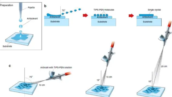
Also in the work Rigas et al. [27] a spray deposition process was investigated, in order to fabricate high-quality organic single crystals based on various semiconducting small molecules on virtually any substrate. This technique, shown schematically in Figure 1.13 combines the advantages of antisolvent crystallization and solution shearing. The authors tested a variety of substrates, among which Si with native oxide, Si with a thermally grown 230 nm SiO2 and flexible polyethylene naphthalate. The devices, that
were fabricated using top and bottom contact approach with TIPS-Pentacene OSSCs grown over the Si/SiO2 substrates, produced good transistor-like behaviour, but not too
high mobility values, up to 0.4 cm2/(Vs) in the linear regime, which indicates that further improvements of the this deposition technique are necessary [27].
18
Figure 1.13: Schematic representation of the deposition technique showed in Rigas et al. [27].
(a) Deposition of antisolvent over the substrate. (b) Shearing mechanism for the droplets, generated by the airbrush, and subsequent formation of single crystals. (c) The shape and size of the crystals are influenced by airbrush position [27].
However, the best mobility for diF-TES-ADT results were obtained in Subramanian et al [28], depositing this molecule from solution by spin-coating, obtaining thus a mobility of 1.5 cm2/(Vs) [28].
In 2013 another heteroacenes, diF-TEG-ADT (2,8-difluorinated
5,11-bis(triethylgermylethynyl)anthradithiophene, Figure 1.14a) was used to fabricate a new type of transistor, as reported in Mei et al. [29]. diF-TEG-ADT is p-type (hole-transporting) semiconductive silylethine-substitued heteroacene in which Ge substitutes previously synthesized Si in diF-TES-ADT, in order to enhance molecular packing [30]. These organic field-effect transistors were fabricated by spin-coating under solvent rich atmosphere (SAC), drop-casting and spray-casting. The substrate is constituted by highly doped silicon, as gate electrode, and thermally grown SiO2 as gate dielectric,
whereas the source and drain Au contacts have been defined photolithographically. The output characteristic for the device realized by drop-casting is reported in Figure 1.14b, while in Figure 1.14c is depicted the transfer characteristics in saturation regime (VD
=-40V); for this class of devices the authors calculated a field-effect mobility μ of 5.4 cm2/(Vs) [29]. In order to realize the devices by spin-coating, the authors dissolved diF-TEG ADT and poly(triarylamine) in tetralin and spin-casted this solution onto a
19
substrate with pre-patterned PFBT-treated Au source and drain electrode, and, in order to enhance the crystallization the as-spun films were annealed [29]. Finally, the authors fabricated spray-coated devices, in order to test the behaviour of diF-TEG-ADT with deposition technique applicable to large-area electronics. The mobilities for the transistors described in Mei et al [29] (realized by drop-casting, spin-coating and spray-casting) are reported in Table 1.1.
Material µdrop-cast (cm2/(Vs)) µspin (cm2/(Vs)) µspray (cm2/(Vs)) diF-TEG-ADT 5.4 3.7 2.2
Table 1.1: Charge carrier mobilities of diF-TEG-ADT in devices fabricated and described in Mei et al
[29].
Figure 1.14: Mei et al [29]: (a) diF-TEG ADT. (b) Output and (c) transfer characteristics for a drop-casting under solvent environment device with L=5 μm and W = 200 μm. Transfer characteristic is measured in the saturation regime (VD=−40 V). Right axis represents log(ID) vs VG, while left axis represents ID1/2 vs VG[29].
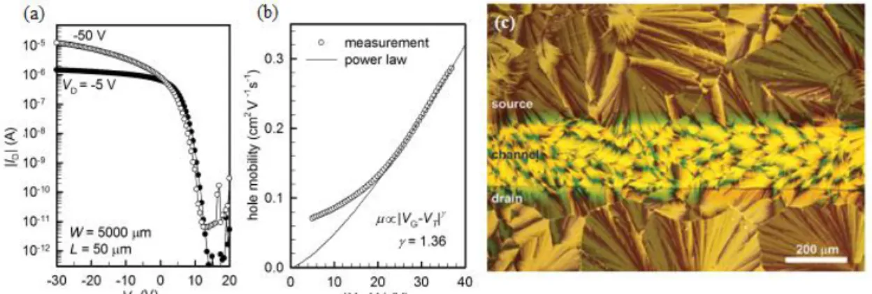
Also the reference Kim et al. [30] presents a kind of device realized by spin-coating of a diF-TEG-ADT solution over a SiO2 substrate. Before the deposition the authors
modified the Au source/drain electrodes by self-assembled monolayers (SAMs) of pentafluorobenzenethiol (PFBT) because of favoured nucleation through F–F, S–F reaction and of enhanced hole injection [30]. Electrical characterization of one of these diF-TEG-ADT OFET is depicted in Figure 1.15a. Transfer characteristics of these devices shows typical p-type field-effect behaviour, and the Ion/Ioff ratio is high, in the
order of 106. In Figure 1.15b, the substantial increase in µ with |VG-VT| indicates that
the charge transport is affected by trap states and/or intrinsic disorder, that the authors mainly attributed to the grain boundaries shown in Figure 1.15c. The authors preferred,
20
to extract mobility, use the transmission-line method (TLM), that provides an indication of the intrinsic properties, instead of the saturation-regime square-root ID method that
has some limitations. The value of µ has been calculated as 0.3 cm2/(Vs) [30].
Figure 1.15: Kim et al. (a) Transfer characteristics of a diF-TEG-ADT OFET. W indicates the channel
width, and L the channel length. (b) VG-dependent hole mobility extracted from the TLM analysis. The solid line is the power-law mobility drawn for comparison. (c) Polarized optical microscope image over a large area, that covers the transistor channel and the adjacent SAM-treated Au electrode regions. [30] .
Another interesting deposition technique applied to TIPS-Pentacene, diF-TES-ADT, 2,7- C8-BTBT (dioctyl[1]benzothieno[3,2-b][1]benzothiophene), and DT-TTF (dithiophene-tetrathiafulvalene), was presented in 2016 in Termiño et al. [31]. This process, named BAMS (bar-assisted meniscus shearing, Figure 1.16), starts with the preparation of solutions of the mentioned semiconductors with PS (Polystyrene) in chlorobenzene. Subsequently a smooth cylindrical bar positioned ≈300 μm above cleaned Si/SiO2 substrates with prefabricated gold electrodes, is employed to cast the
film. In particular a certain volume of the blend solution is deposited between the bar and the substrate, thus a confined meniscus is formed. Then the solution is sheared, therefore the meniscus is displaced, and by convective self-assembly a thin film is formed. This procedure contemplates its realization under ambient conditions. In order to remove any solvent traces, after solution casting the devices are left under vacuum for a certain period of time [32].
21
Figure 1.16: Illustration of the BAMS deposition technique The inset shows an
optical polarized microscopy image exhibiting the formation of large crystalline domains [32].
The polarized optical microscopy images of the films prepared during the work presented in Termiño et al [31] show uniform crystalline domains (Figure 1.17). In particular, TIPS-Pentacene, diF-TES-ADT, and C8-BTBT form spherulitic films with no preferential orientation while, DT-TTF films, on the contrary, are formed by long domains (several millimeter) grown along the shearing direction. Moreover, the sample characterization by X-ray powder diffraction, indicates an high degree of crystallinity [31].
Figure 1.17: Termiño et a [31]: Optical polarized microscopy images of thin films of the four organic semiconductors.
The authors characterized these devices electrically under ambient conditions. Their output characteristics are shown in Figure 1.18. TIPS-Pentacene devices exhibited a
22
small hysteresis between the forward and reverse gate voltage and drain voltage (VD),
however these transistors are characterized by a low average threshold voltage (VT
=-0.9V) and a high average field-effect mobility (μ=1.6 cm2/(Vs)), extracted in saturation regime. Similar values are exhibited by diF-TES-ADT based devices: μ= 1.3 cm2/(Vs) and VT = +0.8 V. C8-BTBT transistors showed instead an average field-effect mobility
of 0.26 cm2/(Vs) and an average threshold voltage of VT=-29 V. Finally, DT-TTF based
devices are characterized by an average field-effect mobility of 0.13 cm2/(Vs), and +3.9
V as average threshold voltage.
Figure 1.18: Termiño et al: Output characteristics of typical devices fabricated with TIPS-PEN, diF-TES-ADT, C8-BTBT and DT-TTF films by BAMS deposition technique. ID is the drain current and the voltage indicated in the plots are the VG voltage at which the device was polarized [31].
Another example of OTFT, realized by drop-casting, mainly for direct detection of X-rays, was reported in the article Lai et al. [33], and it is presented in the following chapter in detail, since it is the device structure employed in the present work.
23
2.
Ionizing radiation detection
Any ionizing radiation detector operates in a manner determined by the way in which the radiation that have to be detected interacts with the material of the detector. The four major categories of ionizing radiation are [34]:
-Heavy charged particles (charged particulate radiations)
-Fast electrons (charged particulate radiations)
-Neutrons (uncharged radiation)
-X-rays and γ-rays (uncharged radiations)
The charged particulate radiations continuously interact through the Coulomb force with the electrons present in any medium which they cross. The uncharged radiations, or indirectly ionizing radiations, on the contrary, are not subjects to the Coulomb force, but they must first undergo an interaction, often involving the nucleus of constituent atoms, that in a single encounter radically changes the properties of incident radiation. In all cases of practical interest, this kind of interaction determines the partial or full transfer of energy of the incident radiation to charged particle products of nuclear reactions, or to the electrons or the nuclei belonging to the constituent atoms. The interaction may not occur within the detector; in this case these radiations pass through the detector volume and they are not detected [34].
X and γ-rays can transfer all or part of its energy to electrons within the medium through several processes, among which, the three most important are described in the following paragraphs. On the contrary, the neutrons involved in an interaction may produce a secondary heavy charged particle, which then serves as the basis of an eventual detector signal [34].
24
2.1.
Ionizing radiation interaction with matter
A large number of interaction mechanism are known for X-rays and γ-rays in matter, but only three major types have an important role in radiation measurements. They are photoelectric absorption, Compton scattering and pair production [10]. These interactions, that have energy-dependent occurrence probability, lead to the partial or complete transfer of the incident photon energy to the electron energy. As a consequence of one of this interaction, the photon may be scattered through a significant angle or may disappear entirely [34].
2.1.1.
Photoelectric absorption
In the photoelectric absorption process a photon has an interaction with an absorber atom. As a result of this interaction the photon completely disappears and a photoelectron having energy Ee is ejected by one of the bound shells of the absorber
atom. Ee is given by the equation (2.1) [34]:
Ee=hν-Eb (2.1)
Where h is the Planck constant, ν the frequency of the incident photon and Eb the binding
energy of the photoelectron. After the interaction, the absorber atom has a vacancy in one of its bound shells, that is can be quickly filled by means of the capture of a free electron from the medium and/or rearrangement of electron belonging to the other shells of the atom. As a result of these processes, one or more characteristics X-rays may also be generated. These X-rays are in most cases reabsorbed close to the original site through the photoelectric absorption, but they can also migrate and escape from detector, thus influencing its response. The photoelectric absorption process is predominant for γ-rays and X-rays of relatively low energy and for absorber materials of high atomic number Z. For this reason there is a preponderance of high Z materials in γ-ray and X-ray shields [34]. A single analytic expression for the probability of photoelectric absorption per atom τph over all ranges of Eph and Z does not exist, but a
25 τph=constant ×
Zn
Eph3.5 (2.2)
Where Z is the atomic number and Eph the incident photon energy.
Over the photon energy region of interest, the exponent n varies between 4 and 5. As indicated by the equation (2.2), the probability of photoelectric absorption is strongly Z dependent. Finally, the photoelectric absorption plays the main role in the mechanism of absorption occurring in X-ray detectors for diagnostic, medical or imaging applications [10].
2.1.2.
Compton scattering
The interaction process known as Compton scattering occurs between a photon incident over an absorbing material and an electron belonging to the absorbing material itself. In this process, shown in Figure 2.1, the incoming photon transfers a portion of its energy to the recoil electron, and it is deflected through an angle θ with respect to its original direction. The energy transferred from the photon to the electron can vary from zero to a large fraction of the γ-ray energy, because all angles of scattering are possible, even if they are not equally probable.It is possible to derive the analytical expression (2.3) that relates the energy transfer and the scattering angle simply by writing simultaneous equations for the conservations of momentum and energy. Using the symbols defined in Figure 2.1 it can be write as [34]:
hv'= hv
1+m hv
0c2(1-cosθ)
(2.3)
Where m0c2 indicates the rest-mass energy of electron (0.511 MeV).
The probability of Compton scattering per atom is a function of the number of electrons available as scattering targets, and it increases linearly with Z. Finally, the angular distribution of scattered γ-rays is given by the Klein-Nishina-formula [34].
26
Figure 2.1: Compton effect [34].
2.1.3.
Pair Production
Pair production is possible if the γ-ray exceeds twice the rest-mass energy of the electron. In this absorption process, the incident photon disappears, and it is replaced by a positron-electron pair. If the impinging photon has an energy larger of 1.02 MeV, that is the energy required to create the pair, its excess energy goes into kinetic energy of the positron and of the electron. After the pair production, the positron annihilates, and then two annihilations photons, that have an important effect on the response of γ-ray detectors, are normally produced as secondary products of interaction. As already mentioned above, the process of pair production is energetically possible if the γ-ray exceed twice the rest-mass energy of the electron, but its probability remains very low until the photon energy is close to several MeV, therefore pair production is mainly confined to high energy γ-rays [34]. The magnitude of the probability of pair productions per nucleus varies approximately as the square of the atomic number-Z. However, no simple expression that describe the probability of this process exists. The Figure 2.2 reports the plot of the relative importance of the three processes described, for different absorber materials and photon energies.
27
Figure 2.2: Relative importance of the three major types of γ-ray
and X-ray interaction described in this chapter. The lines indicate the limits in which the adjacent effects have equal probability [35].
2.2.
Simplified detector model
It is possible to describe a simplified model for a generic detector in which a single particle or quantum radiation undergoes an interaction trough one of the mechanism discussed in the previous paragraphs [34].
In almost all detectors, the net result of the radiation interaction is the appearance of a given amount of electric charge within the detector active volume. This simplified model assumes that a charge Q appears within the detector at time t=0 s as a result of the interaction of a single particle or quantum of radiation. Then, this charge Q must be collected in order to form the basic electrical signal. Often, an electric field within the detector is applied to induce the charges created by the radiation to flow at the opposite directions. The time required to collect the charge is different for each detector type, and it depends on the mobility of the charge carriers within the detector active volume and on the average distance that the charge carriers travel to arrive at the collection electrodes. For example, in ion chambers the collection time can reach few milliseconds, whereas in detectors based on semiconductor diodes its value is of a few nanoseconds. The charge Q, generated in a specific interaction is simply equal to the time integral over the duration of the current described by the equation (2.4) [34]:
∫ I(t)dt=Q
tc
28
Where tc is the charge collection time. The Figure 2.3 presents one example for the
time dependence of the current [34].
Figure 2.3: time dependence for the
detector current [34].
This simplified model contemplates that only one interaction happens at given time, but in any real situation many quanta of radiation will interact over a period of time [34]. Radiation detectors can work in three general modes of operation: pulse mode, current mode and mean square voltage mode. Pulse mode is particularly useful to record each individual quantum of radiation that interacts in the detector. Since the energy deposited in the detector is directly related to Q, normally the time integral of each burst of current or the total charge Q is recorded. A sequence of current bursts is depicted in Figure 2.4. All the detectors that have to measure the energy of individual radiation operate in pulse mode [34].
Figure 2.4: Recorded signal by a current-measuring device,
during a sequence of events [34].
In current mode, the measuring device has a fixed response time T. Therefore, the recorded signal from a sequence of events is a time dependent current given by the equation (2.5):
I(t)=1
T∫ I(t')dt'
t
29
The response time T is typically long compared with the average time that separates the current pulses generated by the incident radiation. Therefore, the detector averages many of the fluctuations in the intervals between individual radiations interactions and it records an average current that depends on the product of the charge per interaction and the interaction rate. In current mode this time average of the individual current bursts is the basic signal [34]. Finally, in the mean square voltage mode of operation the mean square signal, proportional to the square of the charge Q produced in each event, is recorded. This mode of operation is most useful when the measurements are carried out in mixed radiation environments, in which the charge produced by one type of radiation is very different than the one produced by the second type [34].
2.3.
Detection of X-rays and γ-rays
Two different categories of functional materials are used to detect the high energy photons (X-rays and γ-rays): scintillators and semiconductors. In both type of detectors, the high-energy photon causes primary excitations and ionization processes, which, interacting at a second stage within the active volume of the detector, produce electron-hole pairs (excitons) that are transduced into an output signal. This final operation occurs following different pathways in scintillator and semiconductor-based detectors [36]. In a scintillator, the excitons transfer their energy to luminescent centers, often intentionally introduced, that then release this energy radiatively. The resulting photons, typically in the visible wavelength range, are collected by a photodiode or a coupled photo-multiplier tube (PMT), which provide an electrical signal dependent on the incident radiation beam [36]. The visible photons emitted from the scintillator propagates isotropically from the point of generation, thus determining optical crosstalk between pixels in flat-panel detectors, which limits the optical resolution. The resolution in flat-panel detectors is determined by the Modulation Transfer Function (MTF), which, for a given spatial frequency, evaluates the detector ability to transfer the input signal modulation in relation to its output. [37].
In a semiconductor detector, in order to dissociate the electron-hole pairs and to sweep the holes and electrons to the negative and positive electrodes respectively, an electric
30
field is applied. Then, the resulting photocurrent is recorded as the signal associated to the high-energy radiation particles. The direct conversion of ionizing radiation into an electrical signal within the same material, that characterizes the semiconductor-based detectors, allows to achieve better signal-to-noise ratios and device responses time, in comparison with the indirect detection. The both types of detectors require materials characterized by high purity, to minimize exciton trapping, high stopping power, to achieve a high absorption efficiency of the incident radiation, good transparency and good uniformity, in order to reduce scattering. Moreover, the ability to grow these materials into a large size, that allows to increase the interaction volume, constitutes an advantage [36]. A good semiconductor used for detections, is also characterized by [36]:
• High resistivity (>109 Ω·cm) and low leakage current. It is possible to achieve
the necessary high resistivity with high band-gap (>1.5 eV) and low intrinsic carrier concentration.
• A small enough band-gap (<5 eV), in order to have a small electron-hole ionization energy. In this way, the number of electron-hole pairs generated is reasonable large and therefore the signal-to-noise ratio is low.
• High atomic number Z and large interaction volume, in order to obtain an efficient radiation-atomic interaction.
• High intrinsic µτ product, where µ is the carrier mobility and τ is carrier lifetime. • Electrodes must not produce defects, impurities or barriers to the charge collection process, and they must apply a uniform electric field trough the device, in order to avoid material polarization effects, which may have effect on the time response of the detector.
• Surfaces must be highly resistive and stable over time, in order to avoid increases in the surface leakage currents that may occur over the lifetime of the detector.
31
2.4.
Organic direct ionizing radiation
detectors
The first studies about organic direct ionizing radiation detectors started in 2007, with conjugated-polymer-based thin film devices [1]. To date, a good number of direct detectors based on organic semiconductors have been reported. They are based on thin films and single crystal of small molecule, and on organic semiconducting polymers [13] [29] [32] [35]. A description of these works is reports in the following paragraphs. A disadvantage of semiconducting polymers is given by the fact that many polymer-based direct detectors use the measurement of the resistivity (conductivity) of the polymeric semiconductor to evaluate the radiation intensity, which increases (decreases) upon device exposure to the ionizing radiation, in dependence of material degradation. Therefore these devices cannot perform for prolonged periods, and consequently are characterized by a very short operative lifetime [36].
However, as already mentioned in the previous chapter, organic π-conjugated small molecules and polymers are interesting emerging novel material, because they can be deposited by low-cost methods, also at room temperature and over large areas [36].
2.4.1.
Organic Direct Detectors based on Thin Films
A result about flexible detector based on TIPS-Pentacene deposited by drop-casting over an interdigitated structure (Figure 2.5a), and operating at low bias voltage is reported in the article Basiricò et al. [17]. In Figure 2.5 the photocurrent response of this device to the irradiation is depicted. The authors retained that the photocurrent simply due to the charge collection, Icc, would be <2 pA, because of the low photon absorption of the
organic semiconductor. The acquired photocurrent, nevertheless, is about two orders of magnitude bigger (Figure 2.5b), therefore other processes are involved in the generation of such a large photocurrent.
32
Figure 2.5: Basiricò et al. (a) Schematic view of the device. The interdigitated structure is clearly
visible (b) X-ray-induced photocurrent signal of TIPS-Pentacene based detector, polarized at 0.2 V, upon three on/off cycles of a monochromatic synchrotron X-ray beam at 17 keV [17].
The authors ascribe this increase in conductivity to a photoconductive gain, that arises because X-rays generate electron-hole pairs. Electrons remain trapped at the native defects (electron traps) while holes are collected by the electrodes. To maintain charge neutrality in the material multiple holes are emitted to compensate the trapped negative charge, thus enhancing the collected current signal. The amplified photocurrent, given by the photoconductive gain is describe by the equation (2.6):
∆IPG=GICC (2.6)
where G is the photoconductive gain [38].
In the context of this work the authors measured hole mobility in TIPS-pentacene OTFT, before and during an X-rays irradiation, and they observed that it exhibited no significant differences [17], consequently they propose that when this kind of device is exposed to an X-ray beam, additional free carriers are generated and accumulate in the organic thin film.The gold electrodes of this detectors form ohmic contacts with TIPS-Pentacene (the work function of gold, au=(4.7÷5.2) eV [39], is generally considered
matching to HOMO level of TIPS-pentacene that is 5.3 eV [40]), then an increase in carrier concentration ρx determines an increase of current ΔIPG, described by the
equation (2.7) [17]:
33
Where E is the electric field and W the active width of the interdigitated structure [41]. Differences in hole and electron transport in organic materials [42] are useful to derive a model for the increase in free carriers and its impact on X-ray induced photocurrent. This difference can arise from a difference in the charge carrier mobility between electrons and holes or from the presence of traps for one of the two type of charge carriers. In TIPS-Pentacene, hole mobility reaches very high values [19]. On the contrary, electrons are trapped very easily when a polar substrate, like PET [43], is employed and in presence of oxygen [44] [45], that characterizes the measurements carried out in ambient conditions, as in this case. The hypothesis of the authors is therefore that the X-ray generated electrons remain trapped and act as “doping centres”, while the X-ray generated holes drift along the electric field until they reach the collecting electrode. Mobile holes are then continuously re-injected from the injecting electrode, to guarantee charge neutrality. As a result, for each electron-hole pair created more than one hole contributes to the photocurrent, and this fact, that is a sort of “doping” process, leads ultimately to a photoconductive gain [17].
In order to model the experimental saw-tooth shape of the X-ray induced photocurrent, due to an on/off switching X-ray beam (Figure 2.5b), the authors considered the variation of photo-generated carrier concentration ρx in time given by (2.8):
∂ρx(t) ∂t = ϕnq Ah -ρx(t) τr(ρx) (2.8)
The first term in equation (2.8) describes the accumulation of carriers, while the second one describes the recombination of carriers and contains the free carrier lifetime τr(ρx),
that in this paper is approximated by the phenomenological equation (2.9):
τr(ρx)= α γ[αln ( ρ0 ρx)] 1-γ γ (2.9)
Where α, γ and ρ0 are material-specific constants that describe respectively the
characteristic time-scale, the dispersion of trap states, and a reference carrier density. Equation (2.9) models satisfactorily the observed stretched exponential recovery after exposure, while the combined of equations (2.8) and (2.9) fully describe the dynamics of carrier photogeneration and recombination, and the emerging photocurrent during and after X-ray exposure (Figure 2.7a). Experimentally, the sensitivity was determined
34
differentiating the photocurrent data in function of dose rate. Its highest found value is 180 nC/Gy (72000 nC/mGy/cm-3), obtained for low dose-rates and long exposure times. The model reported above allows also to describe the dose rate dependence of the photocurrent, which determines the detector sensitivity, and is in excellent agreement with the results presented in the paper [17].
Figure 2.6: Basiricò et al [17]. Modulation of the conductivity induced by
rays in TIPS-Pentacene thin films. (Left) When the device is not exposed to X-rays the conductivity is due to the intrinsic carriers. (Right) (1) Under X-ray irradiation additional holes and electrons are generated. After generation, holes drift along the electric field until they reach the collecting electrode. (2) On the contrary, the electrons remain trapped in deep trap states within the organic material. (3) Holes are continuously emitted from the injecting electrode to maintain the charge neutrality. (4) Recombination process, that counterbalances the charge photogeneration in the steady-state [17] .
35
Figure 2.7: Basiricò et al. [17]. (a) Dynamic response of the detector under three different
dose rates of radiation: experimental and simulated curves. The device was exposed for 60 s to a synchrotron 17 keV X-ray beam, and polarized at 0.2 V. (b) Photocurrent versus Dose rate plot (scattered points) recorded for different exposure times at the previous conditions. (c) Sensitivity values, calculated differentiating the photocurrent data in function of dose rate, versus dose rate, for different time exposures to the radiation. The solid lines drawn in these plots is the fit of the data, according to the analytical model described above. [17].
The authors evaluated also the mechanical flexibility of the system, characterizing the detectors in a bent configuration with a bending radius of 0.3 cm, that is conformable to the human body curves. The X-ray induced photocurrent was acquired before bending, during bending and after bending, with the substrate restored to a flat conformation. The measurement performed during the first bending evidenced a drop of the X-ray-induced photocurrent of about 50%. On the contrary, between following repetitive measurements on bent and relaxed devices, no significant differences in photocurrent are noticed. Finally, the authors realized an X-ray detection system based on a 2x2 pixelated matrix of organic thin film. The measurements carried out on this device indicate good discrimination between pixels when they are selectively irradiated, making possible the employment of this device for imaging application [17].
36
TIPS-Pentacene was also the base for a novel type of direct thin film detector based on organic transistor, presented in 2017 in Lai et al [33]. The main advantage of this type of sensor is the possibility of tune detection ability acting on the transistor polarization conditions. Moreover, it is possible to integrate the transistor-based sensors in electronic systems, like amplifiers and logic stages, which provide an easy readout of the signals. [33]. Typically, the OFET-based ionizing radiation detectors have relatively high biasing voltages (about a few tens of volts), that limited their development, but the device presented in Lai et al. [33] overcomes this restriction, becoming the first X-ray direct detector based on a low voltage OFET fabricated on a flexible plastic substrate. The transistor structure, based on 175 μm thick, biaxially oriented polyethylene terephthalate (PET) substrate, is explained on detail in the chapter 3, because it is the same used in this work. The semiconductor layer is a polycrystalline film of TIPS-Pentacene, deposited by drop-casting from a solution in toluene, having concentration of wt.0.5% [33]. In Figure 2.8 a typical output and a typical transfer characteristic curves obtained in Lai et al [33] are depicted; they show that the ideal device features, such as significant field-effect modulation, good current saturation, and negligible contact resistance effect are obtained. Moreover, it is noteworthy that drain-to-source and gate-to-source voltages are in the range of 3V, indicating thus that this transistor can work at low voltage. Anyway, a hysteresis and a leakage current are present in the transfer characteristics, but they are very low (the leakage current is about a tens of pA). Finally, the authors calculated mobility values up to 0.1 cm2/(Vs) and a threshold voltage of 0.4V [33].
Figure 2.8: (a) Typical output and (b) transfer characteristic curves of the devices presented in Lai et al.
![Figure 1.3: π-bonding and π*anti-bonding molecular orbitals [7].](https://thumb-eu.123doks.com/thumbv2/123dokorg/7425148.99201/11.892.260.648.507.806/figure-π-bonding-and-anti-bonding-molecular-orbitals.webp)

![Figure 1.9: Output characteristic of an OFET. Linear region and saturation region are indicated [7]](https://thumb-eu.123doks.com/thumbv2/123dokorg/7425148.99201/19.892.223.688.432.710/figure-output-characteristic-linear-region-saturation-region-indicated.webp)
![Figure 1.17: Termiño et a [31]: Optical polarized microscopy images of thin films of the four organic semiconductors](https://thumb-eu.123doks.com/thumbv2/123dokorg/7425148.99201/27.892.273.626.688.968/figure-termiño-optical-polarized-microscopy-images-organic-semiconductors.webp)
![Figure 2.9: Typical response of the low voltage transistor presented in Lai et al.[33] to different dose rates in (a) linear and (b) saturation regimes, as variation in the drain-to-source current](https://thumb-eu.123doks.com/thumbv2/123dokorg/7425148.99201/43.892.151.742.255.467/typical-response-transistor-presented-different-saturation-regimes-variation.webp)
![Figure 2.15: DNN organic single crystals: Optical microscopy image in transmission mode [36]](https://thumb-eu.123doks.com/thumbv2/123dokorg/7425148.99201/49.892.319.586.420.618/figure-organic-single-crystals-optical-microscopy-image-transmission.webp)
![Table 2.1: Carrier mobility values reported in the literature [52] [53] [54] for a 4HCB crystal along the three crystallographic axes, and measured in Fraboni et al [36] for a DNN crystal along the axis of growth [36]](https://thumb-eu.123doks.com/thumbv2/123dokorg/7425148.99201/50.892.135.765.126.282/carrier-mobility-reported-literature-crystallographic-measured-fraboni-crystal.webp)
