Chapter 2
D
ESIGN OF SENSOR
INTERFACES
2.1 Introduction
Complexity of SoC (System on a Chip) design, especially in sensor conditioning applications, has been dramatically increased over the last years thanks to recent advances in integrated technology while time-to-market requirements have been decreased. Cost reduction and performance enhancement of sensors are pushing the introduction of new electronic applications to an increasing variety of fields ranging from monitoring of industrial processes to automotive.
The designer of electronic devices for sensing applications has to provide complex and effective sensor interfaces in a continuously evolving and competitive market. The critical aspects that have to be overcome to achieve final success reside in facing the latest technology facilities, exploiting the recent advances for designing high performance products which combine optimal features with high reliability, answering the market craving for short time to market. A key aspect is also represented by the safety and reliability features that a platform interface has to assure and the need for platform flexibility to guarantee successive upgrading. The design effort for achieving an optimized sensor interface (with regard to area, performances, low power) on one side and the market aggressive demand for low cost and short development cycle has lead to a different series of approaches tailored to the specific application.
2.2 Universal Sensor Interface
During last years, to save development time and reduce design risks, several solutions have been presented, among which the Universal Sensor Interface (USI) [43]. While a full custom ASIC requires considerably design efforts and features higher development costs (both time and money), a more generic and flexible sensor interface can match the market requirements by addressing several similar applications and reducing its costs with a longer production life. This single chip solution has the main advantage to be compatible with a wide range of sensors, but it not tended towards optimal solution for a target sensor. In Figure 2-1 the leading idea of the universal sensor interface is described.
Figure 2-1: Building a Universal Sensor Interface
USI has as drawbacks high power consumption and area occupation, while it features not optimized performances if compared to a chip tailored for a target sensor.
The USI in [46] is implemented with high performance sensor signal acquisition stages, capable of acquiring different typologies of signals (e.g. capacitive, inductive, and resistive). The interface adopts an analog to digital converter based on voltage-to-period technique and processes the data acquired in the digital domain thanks to the presence of a microcontroller and a hardware DSP structure. This interface achieves considerable cost reduction by sharing evaluation resources between different acquisitions from sensors analog interfacing circuits and the actuators [47].
On the other hand, this system does not tend in the direction of any forecasting for a possible customization determined by specific
achieves good performances but not suitable for the strict requirements of demanding application fields like the automotive one.
Figure 2-2: Block diagram of the USI [46].
In literature we can find other solutions such as the Universal Micro-Sensor Interface (UMSI) [45][44] which expands the capability of the USI circuits featuring a sort of sensor bus for connecting the sensor read-out channels to evaluation nodes and embedding standard interface for communication (UART, SPI). In addiction more UMSI can be connected together for achieving an easy implementation of a sensor network. However this approach has the drawback of providing not performing acquisition channel to answer the strict requirements of market demands especially in fields like industrial process monitoring and automotive and aerospace applications
The interfaces implemented in [48] represent an industrial solution for a wide spectrum of sensor applications: piezo-resistive, ceramic-thickfilm, steel-membrane-based (metal-thinfilm), strain-gauge, magneto-resistive bridge sensors. While the solutions proposed in [49] refers to a generic analog conditioning channel suitable for more typologies of sensor and a digital architecture based on general purpose digital blocks handled by microcontroller. This work provide a good flexibility although can handle application which do not require a high degree of complex algorithm for sensor conditioning.
The mentioned approach display the advantages of interfacing a wide class of sensors and to be suitable for many different applications thanks to a little overhead in terms of added circuitry but find their weak point in the sub-optimal architecture which can not guarantee excellent performances and answer the market demands for low power consumption and low area occupation.
2.3 Platform Based Design
The increasing complexity of integrated circuits has lead to a dramatic requested enhance for architectural analysis and the design space exploration The continuous progress of EDA (Electronic Design Automation) tools allows users to speed up the design process but can hardly handle the whole system complexity.
In literature we can find a series of approaches towards the integration of methodologies and strategies in the complete design cycle for achieving the complete design and verification of integrated circuits and answer the market demand for sort development time. To handle the system complexity the most acknowledged approaches reside in the IP-Design and Reuse methodology [50] [51] System Level Design [52] [53], and above all Platform-Based Design approach [54]. All the above mentioned methodologies have been developed to deal with the key issues of modern ASIC design:
• Manufacturing cost: it depends mainly on the area size of
the device, optimizing the area occupation of the chip implies to develop a dedicated architecture for a target application.
• NRE (Non-Recurrent Engineering) cost: it is related to the
design itself and the set of masks of the silicon foundry. The cost of masks is growing rapidly as going to reduced geometries. Moreover testing issues related to modern complex mixed signal ICs are becoming one of the major factor of cost for IC factories.
• Design cost: it is dramatically rising due to the increased
complexity of the new ICs and the challenges caused by distributed physical effects for deep sub-micron technologies. Furthermore design productivity is not keeping the rush with respect to the technology advances making almost impossible to develop the new products facing the increasing complexity and at the same time matching the reduced time to market constraints.
The platform based methodology [55] defines the design of electronic systems from concept to implementation as a sequence of different layer of abstractions in the design flow: each layer can be considered as a platform for which the underlying, subsequent design flow steps are abstracted [56] (see Figure 2-3).
Platform based design exploits rigorously and exhaustively the concepts of design reuse, of design flexibility (the blocks are programmable and are specified at low level), and of correct-by-construction assembly, since modules are pre-characterized and pre-designed (not complete full-custom design). Therefore the platform based methodology features a good cope with manufacturing, NRE and design costs, with little design performance loss.
Figure 2-3: System platform layer and design flow. From system level modeling to prototyping through different layers For embedded system designs, a platform is composed by a library of (preferably configurable) pre-implemented modules, interfaces, services and software that can be assembled to generate a design at that level of abstraction. Each module is provided with a characterization regarding performance and supported features. A platform instance is a set of modules selected from library according to the constraints and the needs specified by the target specifications. Hence this methodology can quickly fulfill a generic class of applications.
Each platform layer can model the upper layers of the platform and in addition it is possible to estimate performance and physical attributes of lower layers in the design flow
Platforms based design found the most important achievement in the definition of the layers, defining design space exploration through regular structure that results in final elimination of large loop of re-design.
On the other hand a critical pace of the platform-based design process is the definition of intermediate platforms to support predictability, for guarantee higher-level optimization, and the design space exploration at high level of abstraction that can condition the whole architecture development.
2.4 Limitations of Platform Based Design flow
The Platform Based methodology represents a powerful strategy for managing complex design with strict constraint subject to development time determined by industrial aggressive markets. However this approach features some weak points with respect to thigh designs imposed by particular application fields, (e.g. critical industrial, aerospace, automotive) that have to be resolved in order to answer the market demand for low cost, low area, high reliability and high performance products.
The key issues of the platform based design are inherent to the architectural design exploration at high design level. The architectural decision have to be taken with the utmost care since all the design will be critically affected by these choices not only for the general architecture but also for preliminary block specifications and for architecture partitioning. This critical aspect recurs also in all top-down design approach. Therefore comprehensive study and exhaustive simulations have to be performed at this highest level of abstraction: the system has to be modelled and even a target sensor has to be taken into account for getting the best possible architecture for the conditioning sensor interface. The critical aspects reside in the unavoidable lack of details by which the system level is affected and little inaccuracies can result in final wrong conditioning chain implementation and in poor specifications for critical blocks. Another killing issue for this approach is determined by unforeseen phenomena in the first level of the design phase which came to light only at the final stage of the design process in the prototyping phase.
All these design issues can determine to a final prototype affected by significant design inaccuracy leading to necessary re-design cycles with a consequent rising of costs and time to market inflation.
Likewise, the missing information details at top system level can lead to a device whose physical implementation does not perfectly match the specification required at the first stage of the design phase, this may occurs for example caused by not accurate simulations (due to the complexity of the product) for performances extraction.
At the extreme consequences, the top-down approach is demonstrated to be critical for all those platform customizations which would require a dedicated feasibility study.
2.5 ISIF platform
The requirement for developing high performances sensor interface with optimal area occupation and low power consumes has pushed towards the research of a new approach for developing platform design methodologies: a new strategy has been developed by the University of Pisa in collaboration with SensorDynamics AG [56][57].
Intelligent Sensor InterFace (ISIF) is a platform for interfacing a generic sensor which has been conceived to overcome the issues related to top-down design methodologies (see section 2.4).
ISIF provides a set of programmable analog and digital IPs directly on silicon that have been developed taking into account the wide-ranging signal conditioning electronics for different sensors. These IPs feature flexible interconnection structure and can be empowered by software routines which can substitute hardware dedicated blocks emulating the hardware IPs and keeping their behavior. With the ISIF platform the optimum architecture can easily be derived from direct evaluation of the target sensor connecting the sensor itself to the platform and performing the analysis directly on silicon. Adopting this approach a various typologies of applications can be evaluated simply by connecting ISIF to the target sensor with a consequent easing and speeding up of the design space exploration phase.
Moreover this approach with the ISIF platform for performing the design space exploration does not exclude a traditional approach to run in parallel: thus MATLAB™ modelling and system level simulations can be performed to achieve a further investigation and possible cross check between the two approaches for system design refinement.
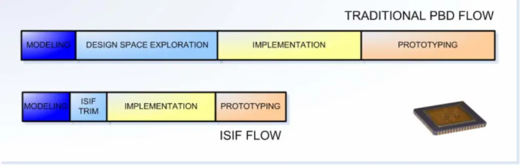
The most important concept that resides in ISIF design flow is represented by the drastic reduction of time needed for performing the design architectural space exploration, which in a traditional platform based design, should have been carried out with the utmost care in a time consuming and error prone process. In place of long time simulations, with ISIF the application can be directly evaluated on the real silicon (thus a prototype of the target application is indeed possible before its actual design). Furthermore accurate feedback information coming from IPs already on silicon can be of crucial importance, since we can observe phenomena impossible to be foreseen in a traditional design simulation. Also a correct evaluation of the real parasitics can be developed thus allowing designers to reach a really accurate estimation of the performance of the device, for
guaranteeing an exact match with the specification of the final product.
Figure 2-4: comparison between design time for a traditional Platform Based and the ISIF flow.
The key aspect to achieve the ISIF concept reside in a twofold feature: the particular care for providing high performance IPs both for analog read-out stage and for digital conditioning path; and the extreme flexibility of the whole structure. In fact not only each single IP can be fully configured but also the routing and the connection map among different IPs can be modified and adjusted, including also the possibility to emulate physical IPs with a library of software routines which perform the same functionalities of hardware IPs and emulate their timing and data-paths limitations. Although ISIF presents some similarities with the Universal Sensor Interface (as it aims to conditioning a wide class of sensors) described in chapter 2.2 it is not tended towards a final product for any target application, its aim is indeed to provide designers a powerful and complete interface for a quick development of a final product with reduced risks and short development time in order to achieve the highest performances and the lowest overheads. This fact entails that only the required analog/digital components are integrated onto the final silicon for production, resulting in minimized area and power overheads. ISIF IPs are in fact tailored not to optimisation of area but have been developed for implementing the platform based design approach keeping as wide as possible the configurability options.
In this way a the architecture space exploration can be rapidly carried out reaching a prototype of the target architecture by simple acquiring the signal by an analog conditioning channel trimming the signal conditioning path with the desired analog IPs (it is possible also to skip some IPs) and then apply complex and ad-hoc algorithm thanks to the hardware DSP structure and the emulation of software IPs. The target sensor can be driven by
several typologies of DAC driver in order to apply a proper feedback implementation.
Furthermore A proper verification methodology has been developed to guarantee the correct system behaviour that will be dealt in chapter 3. ADC DAC DAC C PI ctrl offset comp SENSOR analog digital software input channel demod mod nco
Figure 2-5: example of partitioning of a DSP chain within ISIF platform between analog, digital and software
processing blocks.
ISIF platform has been studied to provide interfacing for capacitive sensors, resistors, to perform measurements of voltages and low currents and many other applications. In the following paragraph, the platform will be presented.
In Figure 2-6 ISIF structure is depicted: the analog front end features a wide range of IPs for sensor signal acquisition, driving and basic analog conditioning such as DACs, ADCs, amplifiers, filters, and current/voltage sources; a digital DSP section based on LEON core; and peripherals for communication with external devices, memories and buses (AMBA APB/AHB). ISIF platform has been developed by SensorDynamics AG in collaboration with Pisa University.
Figure 2-6: ISIF block diagram.
i. Analog section
ISIF analog section features 4 dedicated input channels for sensor signal acquisition (see Figure 2-7). The readout stage is composed by an operational amplifier that can be programmed to implement a charge amplifier, a trans-resistive stage or an instrument amplifier, thus covering a wide range of sensor typologies. Further stages perform signal analog processing, signal recovery, and low-pass filtering for anti-aliasing purpose. Eventually the signal is converted by a 16 bits Sigma Delta ADC. Service circuitries provide voltage/current references, and oscillation for clock generation. The sensor driving stage of the platform is provided by set of configurable 12 bit and 10 bit thermometer DACs. The driving section has been tailored also for creating sinusoidal signals needed for driving a generic sensor. The sine wave is generated by a DAC to create a digitalized wave which can be afterwards filtered with a low pass filter in order to get rid of the spurious harmonic generated by the quantization procedure. DAC references and low pass filter gain can be modified for generating a sine wave with selected amplitude and offset.
The bias section is composed by two regulators, one for the analog 5V supply and one for the 3.3V supply of the digital section, by a bias current generator (developed by a Proportional-To-Absolute-Temperature) and by a current reference.
Figure 2-7: ISIF input channel.
An input/output test bus is provided to supply stimuli and to probe output signals for each block: the test bus represents a key feature for an effective and quick debug of the signal conditioning path. A peculiarity of ISIF analog section is the design accurateness for improving the noise margin, in fact the biasing structure is composed by separated analog and digital power to minimize noise couplings, and particular attention has been applied to the design of the analog IPs that perform sensor signal readout (which is the most critical operation for the sensitivity of the whole system). This system features for noise margin improvement also a JTAG-like approach for handling the digital bits used for analog block configurations, guaranteeing safe communication between digital and analog sections since programming is performed by shifting the configuration bits through shift registers, to overcome clock skew issues.
ii. Digital hardware section
The digital hardware section is based on the LEON core CPU, with related peripherals and dedicated IPs for digital signal processing (see Figure 2-8).
LEON core a 32-bit RISC SPARC-V8 compliant architecture conforming to the IEEE-1754, which features hardware multiplier and divider, interrupt controller, timers, watchdog and memories (ROM, RAM and data/instruction caches); LEON core is freely distributed by European Space Agency under LGPL license, together with standard peripherals for communication with external devices (UARTs, SPIs), and buses (AMBA APB/AHB).
The digital signal processing section is composed by dedicated IPs optimized for low power consumption comprising modulator and channel demodulators, 6 DAC controllers, filters (FIR and IIR) and a Numerical Controlled Oscillator (NCO) capable of providing up to 16 different sine waves with selectable phase with 3 different frequencies.
These IPs feature a flexible interconnection architecture: they are hardware interconnected but they also can be accessed at their input/output by software, thus allowing the designer to implement complex and ad hoc algorithms for the target sensor exploiting this high configurability of DSP section and LEON CPU potentiality, for example a digital PLL has been fully implemented and tested on a fast prototyping board [57].
Figure 2-8: ISIF digital section.
LEON processor is involved in system monitoring, manages signal processing and handles the communication with external devices (such as a PC during the prototyping phase) through available interfaces. The core part of the software is included in ROM (boot and few utility functions), and the functional routines can be downloaded at the start-up phase via UART, or can be stored in an external SPI EEPROM and thus directly reboot from EEPROM. The additional EEPROM can hold different kind of software to be downloaded in order to speed up trimming procedures for achieving an optimized trimming phase, moreover measurements data can be stored to log results.
By using firmware routines the designer can modify interconnections between physical IPs and general settings of each analog and digital IPs for free exploration of design space in the investigation for optimal conditioning architecture. In addiction Firmware utilities can handle the communication with external devices (for debug, monitoring).
iii. Software section
The industrial requirements are pushing towards hardware solution, especially for safety applications, on the other hand digital IPs require detailed and exhaustive analysis to guarantee complete reliability and for proper parameter settings in order to achieve high performances with reasonable area (thus reduced number of trimming bits). Furthermore the presence of non-linearity and parasitic often invalidate the design exploration making a right first time silicon difficult to achieve.
To meet these requirements ISIF platform includes a library of software peripherals (e.g. filters, controllers) with an exact matching with hardware devices. The LEON CPU, thanks to its good signal processing features, guarantees flexibility and required computational power for real-time software IPs implementation. Thus the most common functionalities, which are not physically implemented in the ISIF platform, are modelled by software routines (with the same behaviour of the original DSP library IPs). The DSP software environment features data acquisition from the hardware digital IPs by routines, and inputs data back in further hardware IPs after elaboration just as the data processing was completely hardware-implemented.
These features help the designers to carry on a quick and exhaustive design space exploration changing analog settings, interconnecting digital IPs and even instantiating new ones finding the fittest solution in interfacing a target sensor, both in term of area and performances.
It is worth noticing that ISIF platform is not tended towards a solution with best performances but aims to provide an accurate emulation of a complete hardware interface optimized for the target sensor. In the final ASIC device, software routines can be quickly replaced by corresponding hardware IPs with low risks and costs for redesign, minimizing time to market.
2.6 ISIF physical implementation
ISIF platform has been implemented in a 0.35 µm Bipolar CMOS DMOS technology to perform exhaustive tests on single IP and to check the correct functionality of platform configurations for particular industrial applications.
The main problem in physical implementation has been the analog layout synthesis and the top assembly. A way for speeding up and releasing physical implementation and prototyping phase has been achieved in ISIF platform adopting a modular approach also at the layout level.
Each module is designed and afterward implemented to perform a particular function in the whole sensor interface with the requirements that it is possible to pick it up from the platform to design an interface for a particular class of sensors, and with only minor changes it can fit the final implementation thanks to its optimization for every applications thanks to high level of programmability. However, if necessary, area occupation can be reduced simply cutting a part of the digital programmability which is no more useful since the single cell can be optimized for the target application.
Figure 2-9 shows the physical implementation of the ISIF platform while inFigure 2-10 the final version of ASIC layout is reported, the whole chip area occupation amounts to 72 mm2.
Bibliography
[43] Yong Zhang; Yikang Gu; Vlatkovic, V.; Xiaojuan Wang; Progress of smart sensor and smart sensor networks; Intelligent Control and Automation, 2004. WCICA 2004. Fifth World Congress on , Volume: 4 , 15-19 June 2004 Pages:3600 - 3606 Vol.4.
[44] Jichun Zhang; Kun Zhang; Zhigang Wang; Mason, A.; A Universal Micro-Sensor Interface chip with network communications bus and highly programmable sensor readout; Circuits and Systems, 2002. MWSCAS-2002. The 2002 45th Midwest Symposium on, Volume: 2 , 4-7 Pages:II-246-II-249 Aug. 2002.
[45] Jichun Zhang; Junwei Zhou; Balasundaram, P.; Mason, A.; “A highly programmable sensor network interface with multiple sensor readout circuits Sensors” Proceedings of IEEE , Volume: 2, Pages:748 – 752, 22-24 Oct. 2003
[46] Xiujun Li; Meijer, G.C.M.; de Boer, R.; van der Lee, M.; A high-performance Universal Sensor Interface Sensor for Industry, 2001, Proceedings of the First ISA/IEEE Conference, Pages:19 – 22, 5-7 Nov. 2001
[47] Meijer, G.C.M.; Xiujun LI; “Smart Sensor Interface Electronics”, Microelectronics, 2002. MIEL 2002. 23rd International Conference on, Volume 1, 12-15 May 2002 Page(s):67 - 74 vol.1 [48] ZMD datasheet, http://www.zmda.com/sensor_interfaces.php
[49] K. L. Kraver, M. R. Guthaus, T. D. Strong, P. L. Bird, G. Sig Cha, W. Höld and R. B. Brown, A mixed-signal sensor interface microinstrument, Sensors and Actuators A: Physical, Elsevier Science, 91 (3) (2001) 266-277
[50] D.D. Gajski; A.C.-H. Wu, V. Chaiyakul; S. Mori; T. Nukiyama and P. Bricaud, Essential issues for IP reuse, Proc. of ASP-Design Automation Conference, (2000).
[51] H. Qi; Z. Jiang and J. Wei, IP reusable design methodology, Proc. of International Conference on ASIC, 4 (2001) 756-759
[52] E. Grimpe and F. Oppenheimer, Object-oriented high level synthesis based on SystemC, Proc. of IEEE Int. Conf. on Electronics, Circuits and Systems, (2001) 529-535
[53] T. Grötker, S. Liao, G. Martin, S. Swan, System Design with SystemC, Kluwer Academic Publisher, 2002
[54] Sangiovanni-Vincentelli, A.; Martin, G.; “Platform-based design and software design methodology for embedded systems” Design & Test of Computers, IEEE Volume 18, Issue 6, Nov.-Dec. 2001 Page(s):23 - 33
Solid-State Device Research Conference, 2002. Proceeding of the 32nd European, 24-26 September 2002 Page(s):19 - 30
[56] Fanucci, L.; Giambastiani, A.; Iozzi, F.; Marino, C.; Rocchi, A.; “Platform based design for automotive sensor conditioning” Design, Automation and Test in Europe, 2005. Proceedings 2005 Page(s):186 - 191 Vol. 3.
[57] F. D’Ascoli, M. Tonarelli, M. Melani, M. De Marinis, a. Giambastiani, L. Fanucci, “Intelligent sensor interface for automotive applications” ICECS2005 Gammarth Tunisia Dec 11-14

![Figure 2-2: Block diagram of the USI [46].](https://thumb-eu.123doks.com/thumbv2/123dokorg/7323122.89845/3.723.141.639.182.393/figure-block-diagram-usi.webp)